JP6450367B2 - 光学アセンブリにおける積層素子の歪みを最小限にする方法 - Google Patents
光学アセンブリにおける積層素子の歪みを最小限にする方法 Download PDFInfo
- Publication number
- JP6450367B2 JP6450367B2 JP2016509012A JP2016509012A JP6450367B2 JP 6450367 B2 JP6450367 B2 JP 6450367B2 JP 2016509012 A JP2016509012 A JP 2016509012A JP 2016509012 A JP2016509012 A JP 2016509012A JP 6450367 B2 JP6450367 B2 JP 6450367B2
- Authority
- JP
- Japan
- Prior art keywords
- laminated
- elements
- low
- order
- optical component
- Prior art date
- Legal status (The legal status is an assumption and is not a legal conclusion. Google has not performed a legal analysis and makes no representation as to the accuracy of the status listed.)
- Active
Links
Images







Classifications
-
- G—PHYSICS
- G02—OPTICS
- G02B—OPTICAL ELEMENTS, SYSTEMS OR APPARATUS
- G02B27/00—Optical systems or apparatus not provided for by any of the groups G02B1/00 - G02B26/00, G02B30/00
- G02B27/62—Optical apparatus specially adapted for adjusting optical elements during the assembly of optical systems
-
- B—PERFORMING OPERATIONS; TRANSPORTING
- B23—MACHINE TOOLS; METAL-WORKING NOT OTHERWISE PROVIDED FOR
- B23P—METAL-WORKING NOT OTHERWISE PROVIDED FOR; COMBINED OPERATIONS; UNIVERSAL MACHINE TOOLS
- B23P19/00—Machines for simply fitting together or separating metal parts or objects, or metal and non-metal parts, whether or not involving some deformation; Tools or devices therefor so far as not provided for in other classes
- B23P19/04—Machines for simply fitting together or separating metal parts or objects, or metal and non-metal parts, whether or not involving some deformation; Tools or devices therefor so far as not provided for in other classes for assembling or disassembling parts
-
- G—PHYSICS
- G02—OPTICS
- G02B—OPTICAL ELEMENTS, SYSTEMS OR APPARATUS
- G02B27/00—Optical systems or apparatus not provided for by any of the groups G02B1/00 - G02B26/00, G02B30/00
- G02B27/0012—Optical design, e.g. procedures, algorithms, optimisation routines
-
- G—PHYSICS
- G02—OPTICS
- G02B—OPTICAL ELEMENTS, SYSTEMS OR APPARATUS
- G02B7/00—Mountings, adjusting means, or light-tight connections, for optical elements
- G02B7/003—Alignment of optical elements
- G02B7/004—Manual alignment, e.g. micromanipulators
-
- G—PHYSICS
- G02—OPTICS
- G02B—OPTICAL ELEMENTS, SYSTEMS OR APPARATUS
- G02B7/00—Mountings, adjusting means, or light-tight connections, for optical elements
- G02B7/02—Mountings, adjusting means, or light-tight connections, for optical elements for lenses
- G02B7/025—Mountings, adjusting means, or light-tight connections, for optical elements for lenses using glue
-
- G—PHYSICS
- G02—OPTICS
- G02B—OPTICAL ELEMENTS, SYSTEMS OR APPARATUS
- G02B7/00—Mountings, adjusting means, or light-tight connections, for optical elements
- G02B7/02—Mountings, adjusting means, or light-tight connections, for optical elements for lenses
- G02B7/026—Mountings, adjusting means, or light-tight connections, for optical elements for lenses using retaining rings or springs
-
- G—PHYSICS
- G03—PHOTOGRAPHY; CINEMATOGRAPHY; ANALOGOUS TECHNIQUES USING WAVES OTHER THAN OPTICAL WAVES; ELECTROGRAPHY; HOLOGRAPHY
- G03F—PHOTOMECHANICAL PRODUCTION OF TEXTURED OR PATTERNED SURFACES, e.g. FOR PRINTING, FOR PROCESSING OF SEMICONDUCTOR DEVICES; MATERIALS THEREFOR; ORIGINALS THEREFOR; APPARATUS SPECIALLY ADAPTED THEREFOR
- G03F7/00—Photomechanical, e.g. photolithographic, production of textured or patterned surfaces, e.g. printing surfaces; Materials therefor, e.g. comprising photoresists; Apparatus specially adapted therefor
- G03F7/70—Microphotolithographic exposure; Apparatus therefor
- G03F7/708—Construction of apparatus, e.g. environment aspects, hygiene aspects or materials
- G03F7/70808—Construction details, e.g. housing, load-lock, seals or windows for passing light in or out of apparatus
- G03F7/70825—Mounting of individual elements, e.g. mounts, holders or supports
-
- G—PHYSICS
- G03—PHOTOGRAPHY; CINEMATOGRAPHY; ANALOGOUS TECHNIQUES USING WAVES OTHER THAN OPTICAL WAVES; ELECTROGRAPHY; HOLOGRAPHY
- G03F—PHOTOMECHANICAL PRODUCTION OF TEXTURED OR PATTERNED SURFACES, e.g. FOR PRINTING, FOR PROCESSING OF SEMICONDUCTOR DEVICES; MATERIALS THEREFOR; ORIGINALS THEREFOR; APPARATUS SPECIALLY ADAPTED THEREFOR
- G03F7/00—Photomechanical, e.g. photolithographic, production of textured or patterned surfaces, e.g. printing surfaces; Materials therefor, e.g. comprising photoresists; Apparatus specially adapted therefor
- G03F7/70—Microphotolithographic exposure; Apparatus therefor
- G03F7/708—Construction of apparatus, e.g. environment aspects, hygiene aspects or materials
- G03F7/70975—Assembly, maintenance, transport or storage of apparatus
-
- B—PERFORMING OPERATIONS; TRANSPORTING
- B23—MACHINE TOOLS; METAL-WORKING NOT OTHERWISE PROVIDED FOR
- B23P—METAL-WORKING NOT OTHERWISE PROVIDED FOR; COMBINED OPERATIONS; UNIVERSAL MACHINE TOOLS
- B23P11/00—Connecting or disconnecting metal parts or objects by metal-working techniques not otherwise provided for
-
- G—PHYSICS
- G02—OPTICS
- G02B—OPTICAL ELEMENTS, SYSTEMS OR APPARATUS
- G02B7/00—Mountings, adjusting means, or light-tight connections, for optical elements
- G02B7/003—Alignment of optical elements
-
- Y—GENERAL TAGGING OF NEW TECHNOLOGICAL DEVELOPMENTS; GENERAL TAGGING OF CROSS-SECTIONAL TECHNOLOGIES SPANNING OVER SEVERAL SECTIONS OF THE IPC; TECHNICAL SUBJECTS COVERED BY FORMER USPC CROSS-REFERENCE ART COLLECTIONS [XRACs] AND DIGESTS
- Y10—TECHNICAL SUBJECTS COVERED BY FORMER USPC
- Y10T—TECHNICAL SUBJECTS COVERED BY FORMER US CLASSIFICATION
- Y10T29/00—Metal working
- Y10T29/49—Method of mechanical manufacture
- Y10T29/49764—Method of mechanical manufacture with testing or indicating
- Y10T29/49769—Using optical instrument [excludes mere human eyeballing]
-
- Y—GENERAL TAGGING OF NEW TECHNOLOGICAL DEVELOPMENTS; GENERAL TAGGING OF CROSS-SECTIONAL TECHNOLOGIES SPANNING OVER SEVERAL SECTIONS OF THE IPC; TECHNICAL SUBJECTS COVERED BY FORMER USPC CROSS-REFERENCE ART COLLECTIONS [XRACs] AND DIGESTS
- Y10—TECHNICAL SUBJECTS COVERED BY FORMER USPC
- Y10T—TECHNICAL SUBJECTS COVERED BY FORMER US CLASSIFICATION
- Y10T29/00—Metal working
- Y10T29/49—Method of mechanical manufacture
- Y10T29/49764—Method of mechanical manufacture with testing or indicating
- Y10T29/49771—Quantitative measuring or gauging
-
- Y—GENERAL TAGGING OF NEW TECHNOLOGICAL DEVELOPMENTS; GENERAL TAGGING OF CROSS-SECTIONAL TECHNOLOGIES SPANNING OVER SEVERAL SECTIONS OF THE IPC; TECHNICAL SUBJECTS COVERED BY FORMER USPC CROSS-REFERENCE ART COLLECTIONS [XRACs] AND DIGESTS
- Y10—TECHNICAL SUBJECTS COVERED BY FORMER USPC
- Y10T—TECHNICAL SUBJECTS COVERED BY FORMER US CLASSIFICATION
- Y10T29/00—Metal working
- Y10T29/49—Method of mechanical manufacture
- Y10T29/49764—Method of mechanical manufacture with testing or indicating
- Y10T29/49778—Method of mechanical manufacture with testing or indicating with aligning, guiding, or instruction
- Y10T29/4978—Assisting assembly or disassembly
Landscapes
- Physics & Mathematics (AREA)
- General Physics & Mathematics (AREA)
- Optics & Photonics (AREA)
- Engineering & Computer Science (AREA)
- Environmental & Geological Engineering (AREA)
- Health & Medical Sciences (AREA)
- Epidemiology (AREA)
- Public Health (AREA)
- Mechanical Engineering (AREA)
- Length Measuring Devices By Optical Means (AREA)
- Mounting And Adjusting Of Optical Elements (AREA)
- Testing Of Optical Devices Or Fibers (AREA)
- Lens Barrels (AREA)
- Exposure And Positioning Against Photoresist Photosensitive Materials (AREA)
- Optical Couplings Of Light Guides (AREA)
Description
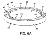
56、58、82、90、92 側面
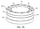
100 光学アセンブリ
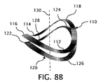
112、114、122、124 ローブ
Claims (10)
- 光学素子を、一定の間隔に置く、位置合わせする、および保持するための、複数の積層素子を含む複合光学部品をアセンブルする方法であって、
光学部品ホルダを含む前記複数の積層素子の、積層面を測定するステップ、
前記積層面の前記測定から主要角振動数を有する数学的近似によって表され得る、低次表面誤差を前記測定から抽出するステップ、
前記積層面どうしを嵌合させた嵌合積層面における、当該積層面の前記低次表面誤差間の相補性を高める相対的配向で、前記光学部品ホルダを含む前記積層素子を相対的に位置付けるステップ、および、
前記相対的配向の前記積層素子の組合せを一緒に固定して、他の相対的配向で前記光学部品ホルダを歪ませることになる応力または歪みを制御するステップ、
を含むことを特徴とする方法。 - 前記積層素子が開口を含み、かつ前記主要角振動数が、前記開口を一周するトレースに沿って前記低次表面誤差が示す、前記積層面から突出しているローブの数に対応し、さらに前記嵌合積層面が、前記開口の周りでπをローブの数で除した分だけ同相で相対的に変位される、一致する数のローブを有していることを特徴とする請求項1記載の方法。
- 前記低次表面誤差が、主要半径方向次数を有し、かつ前記嵌合積層面において相補的な関係にある前記低次表面誤差どうしが、互いに反対符号の共通の主要半径方向次数を有することを特徴とする請求項1記載の方法。
- 任意の残存している相補性のずれに関連する、前記嵌合積層面間の残留している低次表面誤差を判定するステップ、および、
前記嵌合積層面のペアリングを、あるペアリングの前記相補性のずれが別のペアリングの前記相補性のずれに相補的になるように、前記嵌合積層面の他のペアリングに対して配置して、他の場合に前記積層素子の組合せ内で前記光学部品ホルダを歪ませることになる、前記ペアリング間の応力または歪みの蓄積を回避するステップ、
を含むことを特徴とする請求項1記載の方法。 - 他の積層素子に固定された中間積層素子の露出積層面を測定して、主要角振動数を有する数学的近似によって表され得る累積低次誤差を測定するステップ、および、
追加の積層素子と前記中間積層素子との嵌合積層面が、共通の主要角振動数を含む相補的な低次表面誤差を有するように、前記他の積層素子に固定された前記中間積層素子に対して前記追加の積層素子を相対的に配向するステップ、
を含むことを特徴とする請求項1記載の方法。 - 前記測定するステップが前記積層面を測定するステップを含み、かつ前記抽出するステップが、前記測定をフィルタリングして、前記主要角振動数を有する数学的近似によって表され得る前記低次表面誤差の測定を得るステップを含み、さらに、前記嵌合積層面間の前記低次表面誤差の二乗平均平方根が、前記嵌合積層面のいずれかの前記低次表面誤差の二乗平均平方根よりも小さいことを特徴とする請求項1記載の方法。
- 光学素子を、一定の間隔に置く、位置合わせする、および保持するための、複数の積層素子を含む複合光学部品をアセンブルする方法であって、
サブアセンブリの積層素子に固定された中間積層素子の露出積層面を、該露出積層面の累積低次誤差を測定するように測定するステップ、
前記中間積層素子および前記サブアセンブリの積層素子とは別の積層素子であって、前記中間積層素子と隣接して配置される隣接積層素子の側面を、該側面の低次誤差を測定するように測定するステップ、
嵌合する前記中間積層素子の前記露出積層面と前記隣接積層素子の前記側面とが相補的な低次表面誤差を有するように、前記サブアセンブリの前記中間積層素子に対して前記隣接積層素子を相対的に配向するステップ、および、
前記相対的に配向された前記隣接積層素子を、前記サブアセンブリの前記中間積層素子に固定するステップ、
を含むことを特徴とする方法。 - 前記隣接積層素子を前記サブアセンブリに、所与の数の異なる角度位置で固定することができ、前記隣接積層素子が光学部品ホルダであり、さらに、前記隣接積層素子を相対的に配向する前記ステップが、嵌合する前記露出積層面と前記側面との前記低次表面誤差が最も相補的になる前記異なる角度位置を選択するステップを含むことを特徴とする請求項7記載の方法。
- 光学素子を、一定の間隔に置く、位置合わせする、および保持するための、複数の積層素子を含む複合光学部品をアセンブルする方法であって、
光学部品ホルダを含む前記複数の積層素子の、対向する側の積層面を測定するステップ、
前記積層面夫々の前記測定から主要角振動数を有する数学的近似によって表され得る、低次表面誤差を前記測定から抽出するステップ、
前記光学部品ホルダを含む前記積層素子をグループ化するステップであって、当該積層素子の積層面どうしが、組合せとして、かつ互いに相補的な前記低次表面誤差を有して嵌合するよう並置する相対的位置で、グループ化するステップ、および、
前記グループ化による相対的に配向された前記積層素子の前記組合せを一緒に固定して光学アセンブリとし、他の組合せで前記光学部品ホルダを歪ませることになる応力または歪みを最小限にするステップ、
を含むことを特徴とする方法。 - 前記測定するステップが、前記光学アセンブリをアセンブルするのに必要な数より多くの前記積層素子を測定するステップを含み、かつ前記グループ化するステップが、前記積層素子の前記積層面どうしを嵌合したときに、より相補的になる組合せを実現するように、前記積層素子の中から前記光学アセンブリ内に含むものを選択するステップを含むことを特徴とする請求項9記載の方法。
Applications Claiming Priority (5)
| Application Number | Priority Date | Filing Date | Title |
|---|---|---|---|
| US201361812364P | 2013-04-16 | 2013-04-16 | |
| US61/812,364 | 2013-04-16 | ||
| US13/959,804 | 2013-08-06 | ||
| US13/959,804 US9254538B2 (en) | 2013-04-16 | 2013-08-06 | Method of minimizing stacking element distortions in optical assemblies |
| PCT/US2014/033964 WO2014172260A2 (en) | 2013-04-16 | 2014-04-14 | Method of minimizing stacking element distortions in optical assemblies |
Publications (2)
| Publication Number | Publication Date |
|---|---|
| JP2016520862A JP2016520862A (ja) | 2016-07-14 |
| JP6450367B2 true JP6450367B2 (ja) | 2019-01-09 |
Family
ID=51685758
Family Applications (1)
| Application Number | Title | Priority Date | Filing Date |
|---|---|---|---|
| JP2016509012A Active JP6450367B2 (ja) | 2013-04-16 | 2014-04-14 | 光学アセンブリにおける積層素子の歪みを最小限にする方法 |
Country Status (6)
| Country | Link |
|---|---|
| US (2) | US9254538B2 (ja) |
| EP (1) | EP2987022B1 (ja) |
| JP (1) | JP6450367B2 (ja) |
| KR (1) | KR102222390B1 (ja) |
| CN (1) | CN105122117B (ja) |
| WO (1) | WO2014172260A2 (ja) |
Families Citing this family (9)
| Publication number | Priority date | Publication date | Assignee | Title |
|---|---|---|---|---|
| US9254538B2 (en) * | 2013-04-16 | 2016-02-09 | Corning Incorporated | Method of minimizing stacking element distortions in optical assemblies |
| US11035729B1 (en) * | 2014-12-18 | 2021-06-15 | J.A. Woqllam Co., Inc. | Reflectometer, spectrophotometer, ellipsometer and polarimeter system with a super continuum laser source of a beam of electromagnetism, and improved detector system |
| US10132684B1 (en) * | 2014-12-18 | 2018-11-20 | J.A. Woolam Co., Inc. | Reflectometer, spectrophometer, ellipsometer and polarimeter system with a super continuum laser-source of a beam of electromagnetism and improved detector system |
| CN105301795A (zh) * | 2015-10-29 | 2016-02-03 | 中国科学院长春光学精密机械与物理研究所 | 一种高精度共轴光学系统计算机辅助装调及波前检测方法 |
| US10807147B2 (en) * | 2017-01-06 | 2020-10-20 | Korvis Asia Private Limited | Platform for constraining a workpiece on an x-y stage |
| US10732336B2 (en) * | 2017-02-02 | 2020-08-04 | Corning Incorporated | Method of assembling optical systems and minimizing retardance distortions in optical assemblies |
| JP6973280B2 (ja) * | 2018-05-08 | 2021-11-24 | 信越化学工業株式会社 | インプリントモールド用合成石英ガラス基板 |
| EP4285100A4 (en) | 2021-01-29 | 2025-01-01 | J.A. Woollam Co., Inc. | REFLECTOMETER, SPECTROPHOTOMETER, ELLIPSOMETER AND POLARIMETER TYPE SYSTEMS COMPRISING A WAVELENGTH MODIFIER |
| CN121889714A (zh) * | 2023-09-22 | 2026-04-17 | 法格尔光学公司 | 用于确定n个光学元件的组合的装配方案的方法以及由此产生的光学模块 |
Family Cites Families (13)
| Publication number | Priority date | Publication date | Assignee | Title |
|---|---|---|---|---|
| US5428482A (en) | 1991-11-04 | 1995-06-27 | General Signal Corporation | Decoupled mount for optical element and stacked annuli assembly |
| JP3031375B2 (ja) * | 1998-04-23 | 2000-04-10 | キヤノン株式会社 | レンズ鏡筒及びそれを用いた投影露光装置 |
| JP2000066075A (ja) | 1998-08-17 | 2000-03-03 | Nikon Corp | 光学系及びその製造方法、並びに前記光学系を備えた露光装置 |
| DE10146499B4 (de) * | 2001-09-21 | 2006-11-09 | Carl Zeiss Smt Ag | Verfahren zur Optimierung der Abbildungseigenschaften von mindestens zwei optischen Elementen sowie Verfahren zur Optimierung der Abbildungseigenschaften von mindestens drei optischen Elementen |
| US6909493B2 (en) | 2002-03-20 | 2005-06-21 | Canon Kabushiki Kaisha | Correction member, retainer, exposure apparatus, and device fabrication method |
| DE10259599A1 (de) | 2002-12-19 | 2004-07-01 | Carl Zeiss Smt Ag | Verfahren zum Verschrauben von optischen Elementen |
| AU2003219097A1 (en) | 2003-03-26 | 2004-10-18 | Carl Zeiss Smt Ag | Device for the low-deformation replaceable mounting of an optical element |
| DE102006006401A1 (de) * | 2006-02-11 | 2007-08-23 | Carl Zeiss Smt Ag | Verfahren zur Bestimmung der Topographie eines ebenen Körpers sowie zur Herstellung von Fassungen für optische Elemente und Fassung für ein optisches Element |
| JP4823755B2 (ja) * | 2006-04-27 | 2011-11-24 | 富士フイルム株式会社 | レンズシステム組立方法および間隔設定冶具 |
| WO2010074743A1 (en) | 2008-12-22 | 2010-07-01 | Tessera North America, Inc. | Focus compensation for thin cameras |
| DE102010018224A1 (de) | 2010-04-23 | 2012-02-16 | Carl Zeiss Smt Gmbh | Optisches Modul mit einem verstellbaren optischen Element |
| US9254538B2 (en) * | 2013-04-16 | 2016-02-09 | Corning Incorporated | Method of minimizing stacking element distortions in optical assemblies |
| JP2017510849A (ja) * | 2014-04-10 | 2017-04-13 | エムイーエムエス スタート,エルエルシー | ミニチュアレンズアセンブリ及びその製造方法 |
-
2013
- 2013-08-06 US US13/959,804 patent/US9254538B2/en active Active
-
2014
- 2014-04-14 JP JP2016509012A patent/JP6450367B2/ja active Active
- 2014-04-14 EP EP14723654.1A patent/EP2987022B1/en active Active
- 2014-04-14 KR KR1020157032321A patent/KR102222390B1/ko not_active Expired - Fee Related
- 2014-04-14 WO PCT/US2014/033964 patent/WO2014172260A2/en not_active Ceased
- 2014-04-14 CN CN201480021737.XA patent/CN105122117B/zh not_active Expired - Fee Related
-
2016
- 2016-01-18 US US14/997,824 patent/US10137543B2/en active Active
Also Published As
| Publication number | Publication date |
|---|---|
| CN105122117B (zh) | 2018-03-09 |
| US20170057027A1 (en) | 2017-03-02 |
| CN105122117A (zh) | 2015-12-02 |
| EP2987022B1 (en) | 2018-07-04 |
| KR102222390B1 (ko) | 2021-03-04 |
| US9254538B2 (en) | 2016-02-09 |
| KR20150143661A (ko) | 2015-12-23 |
| JP2016520862A (ja) | 2016-07-14 |
| US10137543B2 (en) | 2018-11-27 |
| WO2014172260A3 (en) | 2014-12-24 |
| EP2987022A2 (en) | 2016-02-24 |
| US20140304963A1 (en) | 2014-10-16 |
| WO2014172260A2 (en) | 2014-10-23 |
Similar Documents
| Publication | Publication Date | Title |
|---|---|---|
| JP6450367B2 (ja) | 光学アセンブリにおける積層素子の歪みを最小限にする方法 | |
| JP5481192B2 (ja) | 光学表面の実際形状の所望形状からの偏差を測定する方法および装置 | |
| US20150198438A1 (en) | Diffractive optical element and measuring method | |
| RU2467286C1 (ru) | Устройство юстировки двухзеркальной центрированной оптической системы | |
| WO2010077675A2 (en) | Two grating lateral shearing wavefront sensor | |
| TW201327065A (zh) | 照明光學系統、曝光裝置及元件製造、圖像形成、照明與曝光方法 | |
| KR102178770B1 (ko) | 경사면들에서의 스팟 어레이의 발생 | |
| JP2024505557A (ja) | 補正板を使用した光学システムの収差及びアポダイゼーションの補正 | |
| US8101895B2 (en) | Measurement method, measurement apparatus, and method of manufacturing optical system | |
| JP2003177290A (ja) | ホログラムを使用した光学系整列方法及び装置 | |
| Burge et al. | Measurement of aspheric mirror segments using Fizeau interferometry with CGH correction | |
| Poleshchuk | Computer generated holograms for aspheric optics testing | |
| JP5473743B2 (ja) | 軸外透過波面測定装置 | |
| CN113552097B (zh) | 一种棱镜测试治具及光谱仪 | |
| JP4542108B2 (ja) | セグメントグレーティングアライメント装置 | |
| TW200935041A (en) | Measurement apparatus, exposure apparatus, and device manufacturing method | |
| Foster | Implementation of Phase Induced Apodization Optics on MagAO-X | |
| JP2003214814A (ja) | 干渉測定方法、干渉測定装置、及び投影光学系の製造方法、投影光学系、並びに投影露光装置 | |
| Soto et al. | Development of Hindle array prototype for Keck adaptive secondary mirror | |
| Renault et al. | CRAL expertise on image slicer: optical designs, glass or metallic manufacturing, test and results | |
| EP3351979B1 (en) | Reflecting mirror and mirror holding mechanism | |
| Willingale | Metrology the XEUS mirror plates | |
| Willingale | An alignment and integration scheme for the XEUS mirror plates | |
| JPH0814853A (ja) | 計算機ホログラムを有する平板及びそれを用いた計測 方法 | |
| Gully-Santiago | Innovative technologies for and observational studies of star and planet formation |
Legal Events
| Date | Code | Title | Description |
|---|---|---|---|
| A621 | Written request for application examination |
Free format text: JAPANESE INTERMEDIATE CODE: A621 Effective date: 20170412 |
|
| A131 | Notification of reasons for refusal |
Free format text: JAPANESE INTERMEDIATE CODE: A131 Effective date: 20180306 |
|
| A521 | Request for written amendment filed |
Free format text: JAPANESE INTERMEDIATE CODE: A523 Effective date: 20180606 |
|
| TRDD | Decision of grant or rejection written | ||
| A01 | Written decision to grant a patent or to grant a registration (utility model) |
Free format text: JAPANESE INTERMEDIATE CODE: A01 Effective date: 20181107 |
|
| A61 | First payment of annual fees (during grant procedure) |
Free format text: JAPANESE INTERMEDIATE CODE: A61 Effective date: 20181207 |
|
| R150 | Certificate of patent or registration of utility model |
Ref document number: 6450367 Country of ref document: JP Free format text: JAPANESE INTERMEDIATE CODE: R150 |
|
| R250 | Receipt of annual fees |
Free format text: JAPANESE INTERMEDIATE CODE: R250 |
|
| R250 | Receipt of annual fees |
Free format text: JAPANESE INTERMEDIATE CODE: R250 |
|
| R250 | Receipt of annual fees |
Free format text: JAPANESE INTERMEDIATE CODE: R250 |
|
| R250 | Receipt of annual fees |
Free format text: JAPANESE INTERMEDIATE CODE: R250 |
|
| R250 | Receipt of annual fees |
Free format text: JAPANESE INTERMEDIATE CODE: R250 |