JP6455260B2 - コネクター付き光導波路およびコネクター付き光導波路の製造方法 - Google Patents
コネクター付き光導波路およびコネクター付き光導波路の製造方法 Download PDFInfo
- Publication number
- JP6455260B2 JP6455260B2 JP2015056916A JP2015056916A JP6455260B2 JP 6455260 B2 JP6455260 B2 JP 6455260B2 JP 2015056916 A JP2015056916 A JP 2015056916A JP 2015056916 A JP2015056916 A JP 2015056916A JP 6455260 B2 JP6455260 B2 JP 6455260B2
- Authority
- JP
- Japan
- Prior art keywords
- optical waveguide
- connector
- optical
- main surface
- waveguide
- Prior art date
- Legal status (The legal status is an assumption and is not a legal conclusion. Google has not performed a legal analysis and makes no representation as to the accuracy of the status listed.)
- Active
Links
- 230000003287 optical effect Effects 0.000 title claims description 278
- 238000004519 manufacturing process Methods 0.000 title claims description 26
- 239000013013 elastic material Substances 0.000 claims description 4
- 238000000034 method Methods 0.000 description 21
- 239000000463 material Substances 0.000 description 18
- 238000005253 cladding Methods 0.000 description 13
- 239000000853 adhesive Substances 0.000 description 11
- 230000008569 process Effects 0.000 description 11
- 230000005540 biological transmission Effects 0.000 description 10
- 239000010410 layer Substances 0.000 description 10
- 229920005989 resin Polymers 0.000 description 10
- 239000011347 resin Substances 0.000 description 10
- 230000001070 adhesive effect Effects 0.000 description 9
- 239000012792 core layer Substances 0.000 description 9
- 239000003566 sealing material Substances 0.000 description 9
- JFNLZVQOOSMTJK-KNVOCYPGSA-N norbornene Chemical compound C1[C@@H]2CC[C@H]1C=C2 JFNLZVQOOSMTJK-KNVOCYPGSA-N 0.000 description 7
- 239000000470 constituent Substances 0.000 description 5
- 230000008859 change Effects 0.000 description 4
- 239000003822 epoxy resin Substances 0.000 description 4
- 229920000647 polyepoxide Polymers 0.000 description 4
- 229920000642 polymer Polymers 0.000 description 4
- 238000006116 polymerization reaction Methods 0.000 description 4
- 238000003825 pressing Methods 0.000 description 4
- 230000007613 environmental effect Effects 0.000 description 3
- 239000003505 polymerization initiator Substances 0.000 description 3
- 229920005672 polyolefin resin Polymers 0.000 description 3
- 238000002360 preparation method Methods 0.000 description 3
- 238000007152 ring opening metathesis polymerisation reaction Methods 0.000 description 3
- 239000004593 Epoxy Substances 0.000 description 2
- PXHVJJICTQNCMI-UHFFFAOYSA-N Nickel Chemical compound [Ni] PXHVJJICTQNCMI-UHFFFAOYSA-N 0.000 description 2
- KDLHZDBZIXYQEI-UHFFFAOYSA-N Palladium Chemical compound [Pd] KDLHZDBZIXYQEI-UHFFFAOYSA-N 0.000 description 2
- 238000004891 communication Methods 0.000 description 2
- 239000012141 concentrate Substances 0.000 description 2
- 230000000694 effects Effects 0.000 description 2
- 238000005429 filling process Methods 0.000 description 2
- 239000007788 liquid Substances 0.000 description 2
- 239000005011 phenolic resin Substances 0.000 description 2
- 238000003860 storage Methods 0.000 description 2
- 239000004925 Acrylic resin Substances 0.000 description 1
- 229920000178 Acrylic resin Polymers 0.000 description 1
- 229910000838 Al alloy Inorganic materials 0.000 description 1
- JOYRKODLDBILNP-UHFFFAOYSA-N Ethyl urethane Chemical compound CCOC(N)=O JOYRKODLDBILNP-UHFFFAOYSA-N 0.000 description 1
- 239000004831 Hot glue Substances 0.000 description 1
- 239000004640 Melamine resin Substances 0.000 description 1
- 229920000877 Melamine resin Polymers 0.000 description 1
- 239000004677 Nylon Substances 0.000 description 1
- 239000004952 Polyamide Substances 0.000 description 1
- 239000004642 Polyimide Substances 0.000 description 1
- 239000004793 Polystyrene Substances 0.000 description 1
- VYPSYNLAJGMNEJ-UHFFFAOYSA-N Silicium dioxide Chemical compound O=[Si]=O VYPSYNLAJGMNEJ-UHFFFAOYSA-N 0.000 description 1
- XUIMIQQOPSSXEZ-UHFFFAOYSA-N Silicon Chemical compound [Si] XUIMIQQOPSSXEZ-UHFFFAOYSA-N 0.000 description 1
- 229920001807 Urea-formaldehyde Polymers 0.000 description 1
- NIXOWILDQLNWCW-UHFFFAOYSA-N acrylic acid group Chemical group C(C=C)(=O)O NIXOWILDQLNWCW-UHFFFAOYSA-N 0.000 description 1
- 150000001336 alkenes Chemical class 0.000 description 1
- UMIVXZPTRXBADB-UHFFFAOYSA-N benzocyclobutene Chemical compound C1=CC=C2CCC2=C1 UMIVXZPTRXBADB-UHFFFAOYSA-N 0.000 description 1
- 238000007664 blowing Methods 0.000 description 1
- 239000005388 borosilicate glass Substances 0.000 description 1
- 125000002091 cationic group Chemical group 0.000 description 1
- 150000001768 cations Chemical class 0.000 description 1
- 230000008878 coupling Effects 0.000 description 1
- 238000010168 coupling process Methods 0.000 description 1
- 238000005859 coupling reaction Methods 0.000 description 1
- 125000004122 cyclic group Chemical group 0.000 description 1
- 230000003247 decreasing effect Effects 0.000 description 1
- 238000010586 diagram Methods 0.000 description 1
- 239000011521 glass Substances 0.000 description 1
- 230000017525 heat dissipation Effects 0.000 description 1
- 230000020169 heat generation Effects 0.000 description 1
- 238000005984 hydrogenation reaction Methods 0.000 description 1
- 239000007769 metal material Substances 0.000 description 1
- 239000000203 mixture Substances 0.000 description 1
- 229910052759 nickel Inorganic materials 0.000 description 1
- 125000003518 norbornenyl group Chemical group C12(C=CC(CC1)C2)* 0.000 description 1
- 229920001778 nylon Polymers 0.000 description 1
- JRZJOMJEPLMPRA-UHFFFAOYSA-N olefin Natural products CCCCCCCC=C JRZJOMJEPLMPRA-UHFFFAOYSA-N 0.000 description 1
- 229910052763 palladium Inorganic materials 0.000 description 1
- 230000002093 peripheral effect Effects 0.000 description 1
- 238000005498 polishing Methods 0.000 description 1
- 229920000548 poly(silane) polymer Polymers 0.000 description 1
- 229920002647 polyamide Polymers 0.000 description 1
- 229920002577 polybenzoxazole Polymers 0.000 description 1
- 239000004417 polycarbonate Substances 0.000 description 1
- 229920000515 polycarbonate Polymers 0.000 description 1
- 229920000728 polyester Polymers 0.000 description 1
- 229920001721 polyimide Polymers 0.000 description 1
- 229920001709 polysilazane Polymers 0.000 description 1
- 229920001296 polysiloxane Polymers 0.000 description 1
- 229920002223 polystyrene Polymers 0.000 description 1
- 229910052710 silicon Inorganic materials 0.000 description 1
- 239000010703 silicon Substances 0.000 description 1
- 239000010935 stainless steel Substances 0.000 description 1
- 229910001256 stainless steel alloy Inorganic materials 0.000 description 1
- 239000000126 substance Substances 0.000 description 1
- 125000001424 substituent group Chemical group 0.000 description 1
- 229910052723 transition metal Inorganic materials 0.000 description 1
- 150000003624 transition metals Chemical class 0.000 description 1
- 229920006337 unsaturated polyester resin Polymers 0.000 description 1
- 238000009423 ventilation Methods 0.000 description 1
Images






Landscapes
- Mechanical Coupling Of Light Guides (AREA)
Description
(1) シート状の第1の光導波路と、
シート状の第2の光導波路と、
第1の部材と、第2の部材と、前記第1の部材と前記第2の部材とで画成され、前記第1の光導波路および前記第2の光導波路が挿入されている内腔部とを有するコネクターと、
を備え、
前記第1の光導波路は、前記第1の部材のみに固定され、前記第2の光導波路は、前記第2の部材のみに固定されていることを特徴とするコネクター付き光導波路。
前記内腔部内において、前記第1の光導波路および前記第2の光導波路は、それらの幅方向の両側で、かつ、前記コネクターとの間に設けられた第2の間隙をそれぞれ伴っている上記(2)に記載のコネクター付き光導波路。
(5) 前記媒体は、気体である上記(4)に記載のコネクター付き光導波路。
前記各ガイド孔は、前記第1の部材および前記第2の部材のいずれか一方の部材に設けられている上記(1)ないし(5)のいずれかに記載のコネクター付き光導波路。
互いに表裏の関係にある第1の主面および第2の主面を有するシート状の第2の光導波路と、
第1の部材と、第2の部材と、前記第1の部材と前記第2の部材とで画成され、前記第1の光導波路および前記第2の光導波路が挿入可能な内腔部とを有するコネクターと、を備え、
前記第1の光導波路および前記第2の光導波路は、前記第1の光導波路の前記第1の主面と前記第2の光導波路の前記第2の主面とが対向するように前記内腔部に挿入されており、
前記第1の光導波路の前記第2の主面は、前記第1の部材に固定されるとともに、前記第2の光導波路の前記第1の主面は、前記第2の部材に固定され、
前記第1の光導波路の前記第1の主面は、前記第1の光導波路および前記第2の光導波路よりも弾性が低い低弾性材料に接するとともに、前記第2の光導波路の前記第2の主面は、前記低弾性材料に接していることを特徴とするコネクター付き光導波路。
シート状の第2の光導波路と、
第1の部材と、第2の部材と、前記第1の部材と前記第2の部材とで画成され、前記第1の光導波路および前記第2の光導波路が挿入されている内腔部とを有するコネクターと、を備えるコネクター付き光導波路を製造する製造方法であって、
前記第1の部材に前記第1の光導波路を固定して第1のユニットを得るとともに、前記第2の部材に前記第2の光導波路を固定して第2のユニットを得る工程と、
前記第1のユニットと前記第2のユニットとを組立てて前記コネクター付き光導波路を得る工程と、を備えることを特徴とするコネクター付き光導波路の製造方法。
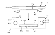
図1は、本発明のコネクター付き光導波路(第1実施形態)を示す斜視図である。図2は、図1中の矢印A方向から見た図である。図3は、図1に示すコネクター付き光導波路の製造方法を説明するための図である。図4は、図1に示すコネクター付き光導波路の製造方法を説明するための図である。
各光導波路3a、3bは、それぞれ同様の構成であるため、以下、1つの光導波路3aについて代表的に説明する。
屈折率差(%)=|A/B−1|×100
コネクター付き光導波路1の製造方法は、用意工程と、固定工程(第1の工程)と、組立工程(第2の工程)と、を有している。
まず、コネクター本体41と蓋体42とを用意する。このとき、コネクター本体41と蓋体42とは、未だ組立てられていない分解状態となっている。
図3に示すように、例えば、接着剤を用いて、蓋体42の突出部421の下面422に光導波路3aの上面31aを固定する。一方、図4に示すように、例えば、接着剤を用いて、コネクター本体41の底板411の底面415に光導波路3bの下面31bを固定する。
図5に示すように、第1ユニット401と第2ユニット402とを組立てる。このとき、底板411および側壁412で囲まれた空間を塞ぐように、蓋体42で覆い、これらの接触面を例えば、接着剤で固定する。
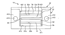
図7および図8は、本発明のコネクター付き光導波路(第2実施形態)の製造方法を説明するための図である。
本実施形態は、主に光導波路の数が異なること以外は第1実施形態と同様である。
図8に示すように、内腔部40に液状の封止材7を充填し、硬化させる。これにより、コネクター付き光導波路1Aを得ることができる。そして、最後に、必要に応じて、コネクター付き光導波路1Aの先端面を研磨する。
図9は、本発明のコネクター付き光導波路の第3実施形態を示す正面図である。
本実施形態は、主にコネクターの形状が異なること以外は第2実施形態と同様である。
図10は、本発明のコネクター付き光導波路の第4実施形態を示す正面図である。
本実施形態は、主にコネクターの形状が異なること以外は第1実施形態と同様である。
2 導光部組立体
21 ガイドピン
3a、3b、3c、3d 光導波路
31a 上面
31b 下面
32 コア層
32a 下面
32b 上面
33a、33b クラッド層
34a、34b、34c、34d、34e コア部
35a、35b、35c、35d、35e、35f 側面クラッド部
4 コネクター
40 内腔部
41 コネクター本体
411 底板
412 側壁
413 ガイド孔
414 凹部
415 底面
42 蓋体
421 突出部
422 下面
423 凹部
5 光導波路
6 コネクター
7 封止材
8 接着剤
10 コネクター付き光導波路組立体
401 第1ユニット
402 第2ユニット
L 線分
S1 間隙
S2 間隙
Claims (9)
- シート状の第1の光導波路と、
シート状の第2の光導波路と、
第1の部材と、第2の部材と、前記第1の部材と前記第2の部材とで画成され、前記第1の光導波路および前記第2の光導波路が挿入されている内腔部とを有するコネクターと、
を備え、
前記第1の光導波路は、前記第1の部材のみに固定され、前記第2の光導波路は、前記第2の部材のみに固定されていることを特徴とするコネクター付き光導波路。 - 前記内腔部内において、前記第1の光導波路および前記第2の光導波路は、向かい合う面の間に設けられた間隙を伴っている請求項1に記載のコネクター付き光導波路。
- 前記間隙を第1の間隙としたとき、
前記内腔部内において、前記第1の光導波路および前記第2の光導波路は、それらの幅方向の両側で、かつ、前記コネクターとの間に設けられた第2の間隙をそれぞれ伴っている請求項2に記載のコネクター付き光導波路。 - 前記第1の間隙および前記第2の間隙には、前記第1の光導波路および前記第2の光導波路よりも弾性率が低い媒体がそれぞれ存在している請求項3に記載のコネクター付き光導波路。
- 前記媒体は、気体である請求項4に記載のコネクター付き光導波路。
- 前記コネクターは、少なくとも2つのガイド孔を有し、
前記各ガイド孔は、前記第1の部材および前記第2の部材のいずれか一方の部材に設けられている請求項1ないし5のいずれか1項に記載のコネクター付き光導波路。 - 前記第1の光導波路および前記第2の光導波路は、それらの端面の法線方向から見たとき、前記各ガイド孔の中心同士を結ぶ線分に対して線対称に配置されている請求項6に記載のコネクター付き光導波路。
- 互いに表裏の関係にある第1の主面および第2の主面を有するシート状の第1の光導波路と、
互いに表裏の関係にある第1の主面および第2の主面を有するシート状の第2の光導波路と、
第1の部材と、第2の部材と、前記第1の部材と前記第2の部材とで画成され、前記第1の光導波路および前記第2の光導波路が挿入可能な内腔部とを有するコネクターと、を備え、
前記第1の光導波路および前記第2の光導波路は、前記第1の光導波路の前記第1の主面と前記第2の光導波路の前記第2の主面とが対向するように前記内腔部に挿入されており、
前記第1の光導波路の前記第2の主面は、前記第1の部材に固定されるとともに、前記第2の光導波路の前記第1の主面は、前記第2の部材に固定され、
前記第1の光導波路の前記第1の主面は、前記第1の光導波路および前記第2の光導波路よりも弾性が低い低弾性材料に接するとともに、前記第2の光導波路の前記第2の主面は、前記低弾性材料に接していることを特徴とするコネクター付き光導波路。 - シート状の第1の光導波路と、
シート状の第2の光導波路と、
第1の部材と、第2の部材と、前記第1の部材と前記第2の部材とで画成され、前記第1の光導波路および前記第2の光導波路が挿入されている内腔部とを有するコネクターと、を備えるコネクター付き光導波路を製造する製造方法であって、
前記第1の部材に前記第1の光導波路を固定して第1のユニットを得るとともに、前記第2の部材に前記第2の光導波路を固定して第2のユニットを得る工程と、
前記第1のユニットと前記第2のユニットとを組立てて前記コネクター付き光導波路を得る工程と、を備えることを特徴とするコネクター付き光導波路の製造方法。
Priority Applications (1)
| Application Number | Priority Date | Filing Date | Title |
|---|---|---|---|
| JP2015056916A JP6455260B2 (ja) | 2015-03-19 | 2015-03-19 | コネクター付き光導波路およびコネクター付き光導波路の製造方法 |
Applications Claiming Priority (1)
| Application Number | Priority Date | Filing Date | Title |
|---|---|---|---|
| JP2015056916A JP6455260B2 (ja) | 2015-03-19 | 2015-03-19 | コネクター付き光導波路およびコネクター付き光導波路の製造方法 |
Publications (2)
| Publication Number | Publication Date |
|---|---|
| JP2016177106A JP2016177106A (ja) | 2016-10-06 |
| JP6455260B2 true JP6455260B2 (ja) | 2019-01-23 |
Family
ID=57071238
Family Applications (1)
| Application Number | Title | Priority Date | Filing Date |
|---|---|---|---|
| JP2015056916A Active JP6455260B2 (ja) | 2015-03-19 | 2015-03-19 | コネクター付き光導波路およびコネクター付き光導波路の製造方法 |
Country Status (1)
| Country | Link |
|---|---|
| JP (1) | JP6455260B2 (ja) |
Families Citing this family (4)
| Publication number | Priority date | Publication date | Assignee | Title |
|---|---|---|---|---|
| TW202323394A (zh) | 2021-08-31 | 2023-06-16 | 日商陶氏東麗股份有限公司 | 顆粒狀硬化性聚矽氧組成物、其硬化物及其製造方法 |
| CN117881747A (zh) | 2021-08-31 | 2024-04-12 | 陶氏东丽株式会社 | 固化性有机硅组合物、其固化物及其制造方法 |
| KR20240051216A (ko) | 2021-08-31 | 2024-04-19 | 다우 도레이 캄파니 리미티드 | 경화성 실리콘 조성물, 그의 경화물, 및 그의 제조방법 |
| WO2024236999A1 (ja) | 2023-05-12 | 2024-11-21 | ダウ・東レ株式会社 | 硬化性シリコーン組成物、その硬化物、およびその製造方法 |
Family Cites Families (8)
| Publication number | Priority date | Publication date | Assignee | Title |
|---|---|---|---|---|
| JP2541011Y2 (ja) * | 1991-07-25 | 1997-07-09 | 日本電信電話株式会社 | 積層型多心一括光ファイバコネクタフェルール |
| JPH08278429A (ja) * | 1995-04-06 | 1996-10-22 | Sumitomo Electric Ind Ltd | 光導波路部品及び光導波路部品の製造方法 |
| JP2907076B2 (ja) * | 1995-09-27 | 1999-06-21 | 日本電気株式会社 | 光導波路デバイス並びにその製造方法 |
| US20040086255A1 (en) * | 2002-10-31 | 2004-05-06 | Botet Alfred D. | Stacked optical fiber arrays |
| JP4933181B2 (ja) * | 2006-07-19 | 2012-05-16 | 三菱電線工業株式会社 | コネクタ付き光ファイバシートおよびその製造方法 |
| KR101272829B1 (ko) * | 2011-06-09 | 2013-06-10 | 한국과학기술원 | 광 연결모듈 및 이를 구비한 광 인쇄회로기판 |
| JP2014130335A (ja) * | 2012-11-30 | 2014-07-10 | Sumitomo Bakelite Co Ltd | 光配線部品および電子機器 |
| US9304264B2 (en) * | 2013-04-26 | 2016-04-05 | Tyco Electronics Corporation | Optical fiber subassembly |
-
2015
- 2015-03-19 JP JP2015056916A patent/JP6455260B2/ja active Active
Also Published As
| Publication number | Publication date |
|---|---|
| JP2016177106A (ja) | 2016-10-06 |
Similar Documents
| Publication | Publication Date | Title |
|---|---|---|
| JP6455260B2 (ja) | コネクター付き光導波路およびコネクター付き光導波路の製造方法 | |
| JP6678112B2 (ja) | 光コネクタ | |
| JP6952041B2 (ja) | 導波路アクセス不可能スペースを有する光フェルール | |
| CN103676032B (zh) | 连接器及其制造方法和光学通信系统 | |
| CA2807122C (en) | Optical component | |
| JP2014130335A (ja) | 光配線部品および電子機器 | |
| US7350982B2 (en) | Sub-mount for mounting optical component and light transmission and reception module | |
| JP5096651B2 (ja) | 熱張係数の異なる材料間の低応力界面及びその製造方法 | |
| JP6514929B2 (ja) | 光ファイバ付きフェルール及び光コネクタシステム | |
| JP7087351B2 (ja) | 光配線部品および電子機器 | |
| JP2016018165A (ja) | 光配線部品、光導波路組立体および光配線部品の製造方法 | |
| CN110770618B (zh) | 光纤构件 | |
| JP2018005179A (ja) | 光コネクター、光伝送体、コネクター付き光伝送体および電子機器 | |
| JP6904213B2 (ja) | 光ファイバ保持具 | |
| JP5281058B2 (ja) | 光部品 | |
| JP6196583B2 (ja) | 光モジュール | |
| JP7491102B2 (ja) | 光分配器および電子機器 | |
| JP2018180046A (ja) | 光ファイバ部材 | |
| JP2018097287A (ja) | 光配線部品および電子機器 | |
| JP2005024782A (ja) | 光導波路パッケージ | |
| JP3902058B2 (ja) | 光モジュール | |
| JP5994525B2 (ja) | 光モジュール | |
| JP4968677B2 (ja) | 光路変換素子 | |
| JP2016206308A (ja) | 光接続部品 | |
| JP2008281695A (ja) | 光導波路及び光導波路基板 |
Legal Events
| Date | Code | Title | Description |
|---|---|---|---|
| A621 | Written request for application examination |
Free format text: JAPANESE INTERMEDIATE CODE: A621 Effective date: 20180209 |
|
| A977 | Report on retrieval |
Free format text: JAPANESE INTERMEDIATE CODE: A971007 Effective date: 20181112 |
|
| TRDD | Decision of grant or rejection written | ||
| A01 | Written decision to grant a patent or to grant a registration (utility model) |
Free format text: JAPANESE INTERMEDIATE CODE: A01 Effective date: 20181120 |
|
| A61 | First payment of annual fees (during grant procedure) |
Free format text: JAPANESE INTERMEDIATE CODE: A61 Effective date: 20181203 |
|
| R150 | Certificate of patent or registration of utility model |
Ref document number: 6455260 Country of ref document: JP Free format text: JAPANESE INTERMEDIATE CODE: R150 |