JP6465251B2 - 電子機器 - Google Patents
電子機器 Download PDFInfo
- Publication number
- JP6465251B2 JP6465251B2 JP2018509145A JP2018509145A JP6465251B2 JP 6465251 B2 JP6465251 B2 JP 6465251B2 JP 2018509145 A JP2018509145 A JP 2018509145A JP 2018509145 A JP2018509145 A JP 2018509145A JP 6465251 B2 JP6465251 B2 JP 6465251B2
- Authority
- JP
- Japan
- Prior art keywords
- conductor
- transmission line
- circuit board
- electronic device
- signal
- Prior art date
- Legal status (The legal status is an assumption and is not a legal conclusion. Google has not performed a legal analysis and makes no representation as to the accuracy of the status listed.)
- Active
Links
Images


Classifications
-
- H—ELECTRICITY
- H05—ELECTRIC TECHNIQUES NOT OTHERWISE PROVIDED FOR
- H05K—PRINTED CIRCUITS; CASINGS OR CONSTRUCTIONAL DETAILS OF ELECTRIC APPARATUS; MANUFACTURE OF ASSEMBLAGES OF ELECTRICAL COMPONENTS
- H05K1/00—Printed circuits
- H05K1/02—Details
- H05K1/0213—Electrical arrangements not otherwise provided for
- H05K1/0237—High frequency adaptations
- H05K1/0242—Structural details of individual signal conductors, e.g. related to the skin effect
-
- H—ELECTRICITY
- H01—ELECTRIC ELEMENTS
- H01P—WAVEGUIDES; RESONATORS, LINES, OR OTHER DEVICES OF THE WAVEGUIDE TYPE
- H01P3/00—Waveguides; Transmission lines of the waveguide type
- H01P3/02—Waveguides; Transmission lines of the waveguide type with two longitudinal conductors
- H01P3/08—Microstrips; Strip lines
-
- H—ELECTRICITY
- H01—ELECTRIC ELEMENTS
- H01P—WAVEGUIDES; RESONATORS, LINES, OR OTHER DEVICES OF THE WAVEGUIDE TYPE
- H01P3/00—Waveguides; Transmission lines of the waveguide type
- H01P3/02—Waveguides; Transmission lines of the waveguide type with two longitudinal conductors
- H01P3/08—Microstrips; Strip lines
- H01P3/081—Microstriplines
-
- H—ELECTRICITY
- H01—ELECTRIC ELEMENTS
- H01P—WAVEGUIDES; RESONATORS, LINES, OR OTHER DEVICES OF THE WAVEGUIDE TYPE
- H01P3/00—Waveguides; Transmission lines of the waveguide type
- H01P3/02—Waveguides; Transmission lines of the waveguide type with two longitudinal conductors
- H01P3/08—Microstrips; Strip lines
- H01P3/085—Triplate lines
-
- H—ELECTRICITY
- H05—ELECTRIC TECHNIQUES NOT OTHERWISE PROVIDED FOR
- H05K—PRINTED CIRCUITS; CASINGS OR CONSTRUCTIONAL DETAILS OF ELECTRIC APPARATUS; MANUFACTURE OF ASSEMBLAGES OF ELECTRICAL COMPONENTS
- H05K1/00—Printed circuits
- H05K1/02—Details
- H05K1/0213—Electrical arrangements not otherwise provided for
- H05K1/0216—Reduction of cross-talk, noise or electromagnetic interference
- H05K1/0218—Reduction of cross-talk, noise or electromagnetic interference by printed shielding conductors, ground planes or power plane
- H05K1/0219—Printed shielding conductors for shielding around or between signal conductors, e.g. coplanar or coaxial printed shielding conductors
- H05K1/0221—Coaxially shielded signal lines comprising a continuous shielding layer partially or wholly surrounding the signal lines
-
- H—ELECTRICITY
- H05—ELECTRIC TECHNIQUES NOT OTHERWISE PROVIDED FOR
- H05K—PRINTED CIRCUITS; CASINGS OR CONSTRUCTIONAL DETAILS OF ELECTRIC APPARATUS; MANUFACTURE OF ASSEMBLAGES OF ELECTRICAL COMPONENTS
- H05K1/00—Printed circuits
- H05K1/02—Details
- H05K1/11—Printed elements for providing electric connections to or between printed circuits
Landscapes
- Engineering & Computer Science (AREA)
- Microelectronics & Electronic Packaging (AREA)
- Physics & Mathematics (AREA)
- Electromagnetism (AREA)
- Structure Of Printed Boards (AREA)
- Waveguides (AREA)
Description
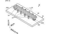
20,20A,20B,20C:伝送線路
21,21B:基材
30,30A,30B,30C:回路基板
31,31C:基板本体
33:導体柱
33A:輻射抑制導体
35:グランド導体
40:高周波モジュール
41,42:電子部品
201C:第1伝送部
202C:第2伝送部
203C:第3伝送部
211,212,213,211A:誘電体シート
221,222,221A:絶縁性保護膜
231:信号導体
2321,2322:コネクタ
241,242:グランド導体
251:第1外部接続導体
252:第2外部接続導体
253:穴
253B:グランド接続用導体
261,262:層間接続導体
280:グランド用補助導体
281:層間接続導体
300,300C:凹部
321,322:コネクタ
341:第1実装ランド導体
342:第2実装ランド導体
343:グランド用ランド導体
350:凹部
411:送信回路
412:送信フィルタ
413:受信フィルタ
414:受信回路
2711,2721,2712,2722:穴
ANT:アンテナ
Claims (11)
- 信号導体を備える伝送線路と、該伝送線路が実装される回路基板と、を備える電子機器であって、
前記伝送線路は、
第1主面、第2主面、および、前記信号導体の延びる方向に沿った第1側面と第2側面とを有し、可撓性を有する基材と、
前記基材に形成された前記信号導体と、
前記信号導体の信号伝送方向の第1端に接続され、前記基材の前記第1主面に形成された第1外部接続導体と、
前記信号導体の前記信号伝送方向の第2端に接続され、前記基材の前記第1主面に形成された第2外部接続導体と、
前記基材の厚み方向において、前記信号導体から離間して形成されたグランド導体と、を備え、
前記回路基板は、
前記第1外部接続導体が接続される第1実装ランド導体と、
前記第2外部接続導体が接続される第2実装ランド導体と、
実装された前記伝送線路の前記第1側面と前記第2側面とに沿って設けられ、前記第1側面と前記第2側面に当接または近接する輻射抑制導体と、を備える、
電子機器。 - 前記輻射抑制導体は、それぞれが前記回路基板の表面から突出する形状であり、前記第1側面および前記第2側面に沿って間隔を空けて配列された複数の導体柱である、
請求項1に記載の電子機器。 - 前記複数の導体柱のそれぞれの高さは、前記表面から前記第2主面までの距離以上である、
請求項2に記載の電子機器。 - 前記回路基板は、
前記伝送線路に応じた形状であって、前記回路基板の表面から凹む第1凹部を備え、
前記伝送線路は前記第1凹部に少なくとも部分的に埋まっており、
前記輻射抑制導体は、前記第1凹部の側面に形成されている、
請求項1に記載の電子機器。 - 前記第1凹部の底面には、前記第1主面を平面視して、前記信号導体に重なる第2凹部を備え、
前記第2凹部には、グランド導体が形成されている、
請求項4に記載の電子機器。 - 前記第1凹部の側面の高さは、前記伝送線路の厚み以上である、
請求項4または請求項5に記載の電子機器。 - 前記第1外部接続導体と前記第1実装ランド導体とは、直接に接合され、
前記第2外部接続導体と前記第2実装ランド導体とは、直接に接合されている、
請求項1乃至請求項6のいずれかに記載の電子機器。 - 前記伝送線路は、前記第1主面に、前記信号導体の延びる方向に沿って配置された複数の補助グランド接続導体を備え、
前記回路基板は、複数のグランド用ランド導体を備え、
前記複数の補助グランド接続導体は、前記複数のグランド用ランド導体にそれぞれ接続されている、
請求項7に記載の電子機器。 - 前記伝送線路の前記基材の比誘電率は、前記回路基板の比誘電率よりも低い、
請求項1乃至請求項8のいずれかに記載の電子機器。 - 前記伝送線路は、前記第1主面を平面視して前記信号伝送方向が変化する、前記信号導体の横曲がり部を有する、
請求項1乃至請求項9のいずれかに記載の電子機器。 - 前記伝送線路は、前記第1主面を側面視して前記信号伝送方向が変化する、前記信号導体の縦曲がり部を有する、
請求項1乃至請求項10のいずれかに記載の電子機器。
Applications Claiming Priority (3)
| Application Number | Priority Date | Filing Date | Title |
|---|---|---|---|
| JP2016074242 | 2016-04-01 | ||
| JP2016074242 | 2016-04-01 | ||
| PCT/JP2017/011578 WO2017170074A1 (ja) | 2016-04-01 | 2017-03-23 | 電子機器 |
Publications (2)
| Publication Number | Publication Date |
|---|---|
| JPWO2017170074A1 JPWO2017170074A1 (ja) | 2018-07-26 |
| JP6465251B2 true JP6465251B2 (ja) | 2019-02-06 |
Family
ID=59964400
Family Applications (1)
| Application Number | Title | Priority Date | Filing Date |
|---|---|---|---|
| JP2018509145A Active JP6465251B2 (ja) | 2016-04-01 | 2017-03-23 | 電子機器 |
Country Status (4)
| Country | Link |
|---|---|
| US (1) | US10524354B2 (ja) |
| JP (1) | JP6465251B2 (ja) |
| CN (1) | CN209314132U (ja) |
| WO (1) | WO2017170074A1 (ja) |
Families Citing this family (1)
| Publication number | Priority date | Publication date | Assignee | Title |
|---|---|---|---|---|
| JP7066772B2 (ja) * | 2020-03-26 | 2022-05-13 | 株式会社日立製作所 | 信号伝送回路およびプリント基板 |
Family Cites Families (9)
| Publication number | Priority date | Publication date | Assignee | Title |
|---|---|---|---|---|
| JPS6454901A (en) * | 1987-08-26 | 1989-03-02 | Matsushita Electric Industrial Co Ltd | Filter circuit device for strip line |
| CA2418674A1 (en) * | 2003-02-07 | 2004-08-07 | Tak Shun Cheung | Transmission lines and transmission line components with wavelength reduction and shielding |
| JP2005012727A (ja) * | 2003-06-23 | 2005-01-13 | Kyocera Corp | 高周波用伝送線路 |
| WO2005065000A1 (en) * | 2003-12-24 | 2005-07-14 | Molex Incorporated | Electromagnetically shielded slot transmission line |
| JP2010103982A (ja) | 2008-09-25 | 2010-05-06 | Sony Corp | ミリ波伝送装置、ミリ波伝送方法、ミリ波伝送システム |
| WO2012073591A1 (ja) * | 2010-12-03 | 2012-06-07 | 株式会社村田製作所 | 高周波信号線路 |
| CN103906348B (zh) * | 2010-12-03 | 2017-11-24 | 株式会社村田制作所 | 电子设备 |
| JP5574056B2 (ja) | 2011-11-10 | 2014-08-20 | 株式会社村田製作所 | 高周波信号線路及びこれを備えた電子機器 |
| CN205584615U (zh) * | 2013-12-12 | 2016-09-14 | 株式会社村田制作所 | 信号传输元器件及电子设备 |
-
2017
- 2017-03-23 CN CN201790000636.3U patent/CN209314132U/zh active Active
- 2017-03-23 WO PCT/JP2017/011578 patent/WO2017170074A1/ja not_active Ceased
- 2017-03-23 JP JP2018509145A patent/JP6465251B2/ja active Active
-
2018
- 2018-08-23 US US16/109,918 patent/US10524354B2/en active Active
Also Published As
| Publication number | Publication date |
|---|---|
| JPWO2017170074A1 (ja) | 2018-07-26 |
| US20180368252A1 (en) | 2018-12-20 |
| WO2017170074A1 (ja) | 2017-10-05 |
| US10524354B2 (en) | 2019-12-31 |
| CN209314132U (zh) | 2019-08-27 |
Similar Documents
| Publication | Publication Date | Title |
|---|---|---|
| US10770773B2 (en) | Electronic apparatus | |
| US10424432B2 (en) | Inductor bridge and electronic device | |
| JP6156610B2 (ja) | 電子機器、およびアンテナ素子 | |
| US10038231B2 (en) | Signal transmission component and electronic device | |
| US9699895B2 (en) | Flexible board and electronic device | |
| US8289728B2 (en) | Interconnect board, printed circuit board unit, and method | |
| US9705194B2 (en) | Antenna module | |
| US10756462B2 (en) | Resin multilayer substrate and an electronic device and a joint structure of a resin multilayer substrate | |
| JP6137360B2 (ja) | 高周波線路及び電子機器 | |
| CN104798248A (zh) | 传输线路及电子设备 | |
| US20110080717A1 (en) | Interconnect board, printed circuit board unit, and method | |
| US10772204B2 (en) | Electronic device | |
| KR20190099709A (ko) | 인쇄회로기판 | |
| JPWO2017170074A1 (ja) | 電子機器 | |
| US20150022288A1 (en) | High-frequency signal line | |
| JP4665698B2 (ja) | アンテナ装置 | |
| JP6848119B1 (ja) | 複合配線基板、パッケージおよび電子機器 |
Legal Events
| Date | Code | Title | Description |
|---|---|---|---|
| A621 | Written request for application examination |
Free format text: JAPANESE INTERMEDIATE CODE: A621 Effective date: 20180411 |
|
| A871 | Explanation of circumstances concerning accelerated examination |
Free format text: JAPANESE INTERMEDIATE CODE: A871 Effective date: 20180411 |
|
| A975 | Report on accelerated examination |
Free format text: JAPANESE INTERMEDIATE CODE: A971005 Effective date: 20180709 |
|
| A131 | Notification of reasons for refusal |
Free format text: JAPANESE INTERMEDIATE CODE: A131 Effective date: 20180717 |
|
| A521 | Request for written amendment filed |
Free format text: JAPANESE INTERMEDIATE CODE: A523 Effective date: 20180912 |
|
| TRDD | Decision of grant or rejection written | ||
| A01 | Written decision to grant a patent or to grant a registration (utility model) |
Free format text: JAPANESE INTERMEDIATE CODE: A01 Effective date: 20181211 |
|
| A61 | First payment of annual fees (during grant procedure) |
Free format text: JAPANESE INTERMEDIATE CODE: A61 Effective date: 20181224 |
|
| R150 | Certificate of patent or registration of utility model |
Ref document number: 6465251 Country of ref document: JP Free format text: JAPANESE INTERMEDIATE CODE: R150 |