JP6477894B2 - 樹脂回路基板、部品搭載樹脂回路基板 - Google Patents
樹脂回路基板、部品搭載樹脂回路基板 Download PDFInfo
- Publication number
- JP6477894B2 JP6477894B2 JP2017538032A JP2017538032A JP6477894B2 JP 6477894 B2 JP6477894 B2 JP 6477894B2 JP 2017538032 A JP2017538032 A JP 2017538032A JP 2017538032 A JP2017538032 A JP 2017538032A JP 6477894 B2 JP6477894 B2 JP 6477894B2
- Authority
- JP
- Japan
- Prior art keywords
- component
- circuit board
- conductor
- resin
- mounting land
- Prior art date
- Legal status (The legal status is an assumption and is not a legal conclusion. Google has not performed a legal analysis and makes no representation as to the accuracy of the status listed.)
- Active
Links
Images


Classifications
-
- H—ELECTRICITY
- H05—ELECTRIC TECHNIQUES NOT OTHERWISE PROVIDED FOR
- H05K—PRINTED CIRCUITS; CASINGS OR CONSTRUCTIONAL DETAILS OF ELECTRIC APPARATUS; MANUFACTURE OF ASSEMBLAGES OF ELECTRICAL COMPONENTS
- H05K1/00—Printed circuits
- H05K1/18—Printed circuits structurally associated with non-printed electric components
- H05K1/182—Printed circuits structurally associated with non-printed electric components associated with components mounted in printed circuit boards [PCB], e.g. insert-mounted components [IMC]
- H05K1/183—Printed circuits structurally associated with non-printed electric components associated with components mounted in printed circuit boards [PCB], e.g. insert-mounted components [IMC] associated with components mounted in and supported by recessed areas of the PCBs
-
- H—ELECTRICITY
- H05—ELECTRIC TECHNIQUES NOT OTHERWISE PROVIDED FOR
- H05K—PRINTED CIRCUITS; CASINGS OR CONSTRUCTIONAL DETAILS OF ELECTRIC APPARATUS; MANUFACTURE OF ASSEMBLAGES OF ELECTRICAL COMPONENTS
- H05K1/00—Printed circuits
- H05K1/02—Details
- H05K1/0213—Electrical arrangements not otherwise provided for
- H05K1/0216—Reduction of cross-talk, noise or electromagnetic interference
- H05K1/023—Reduction of cross-talk, noise or electromagnetic interference using auxiliary mounted passive components or auxiliary substances
- H05K1/0231—Capacitors or dielectric substances
-
- H—ELECTRICITY
- H05—ELECTRIC TECHNIQUES NOT OTHERWISE PROVIDED FOR
- H05K—PRINTED CIRCUITS; CASINGS OR CONSTRUCTIONAL DETAILS OF ELECTRIC APPARATUS; MANUFACTURE OF ASSEMBLAGES OF ELECTRICAL COMPONENTS
- H05K1/00—Printed circuits
- H05K1/18—Printed circuits structurally associated with non-printed electric components
- H05K1/182—Printed circuits structurally associated with non-printed electric components associated with components mounted in printed circuit boards [PCB], e.g. insert-mounted components [IMC]
- H05K1/185—Printed circuits structurally associated with non-printed electric components associated with components mounted in printed circuit boards [PCB], e.g. insert-mounted components [IMC] associated with components encapsulated in the insulating substrate of the PCBs; associated with components incorporated in internal layers of multilayer circuit boards
- H05K1/186—Printed circuits structurally associated with non-printed electric components associated with components mounted in printed circuit boards [PCB], e.g. insert-mounted components [IMC] associated with components encapsulated in the insulating substrate of the PCBs; associated with components incorporated in internal layers of multilayer circuit boards manufactured by mounting on or connecting to patterned circuits before or during embedding
-
- H—ELECTRICITY
- H05—ELECTRIC TECHNIQUES NOT OTHERWISE PROVIDED FOR
- H05K—PRINTED CIRCUITS; CASINGS OR CONSTRUCTIONAL DETAILS OF ELECTRIC APPARATUS; MANUFACTURE OF ASSEMBLAGES OF ELECTRICAL COMPONENTS
- H05K3/00—Apparatus or processes for manufacturing printed circuits
- H05K3/46—Manufacturing multilayer circuits
- H05K3/4611—Manufacturing multilayer circuits by laminating two or more circuit boards
- H05K3/4614—Manufacturing multilayer circuits by laminating two or more circuit boards the electrical connections between the circuit boards being made during lamination
-
- H—ELECTRICITY
- H10—SEMICONDUCTOR DEVICES; ELECTRIC SOLID-STATE DEVICES NOT OTHERWISE PROVIDED FOR
- H10W—GENERIC PACKAGES, INTERCONNECTIONS, CONNECTORS OR OTHER CONSTRUCTIONAL DETAILS OF DEVICES COVERED BY CLASS H10
- H10W70/00—Package substrates; Interposers; Redistribution layers [RDL]
- H10W70/60—Insulating or insulated package substrates; Interposers; Redistribution layers
- H10W70/62—Insulating or insulated package substrates; Interposers; Redistribution layers characterised by their interconnections
- H10W70/63—Vias, e.g. via plugs
- H10W70/635—Through-vias
-
- H—ELECTRICITY
- H10—SEMICONDUCTOR DEVICES; ELECTRIC SOLID-STATE DEVICES NOT OTHERWISE PROVIDED FOR
- H10W—GENERIC PACKAGES, INTERCONNECTIONS, CONNECTORS OR OTHER CONSTRUCTIONAL DETAILS OF DEVICES COVERED BY CLASS H10
- H10W70/00—Package substrates; Interposers; Redistribution layers [RDL]
- H10W70/60—Insulating or insulated package substrates; Interposers; Redistribution layers
- H10W70/67—Insulating or insulated package substrates; Interposers; Redistribution layers characterised by their insulating layers or insulating parts
- H10W70/68—Shapes or dispositions thereof
- H10W70/685—Shapes or dispositions thereof comprising multiple insulating layers
-
- H—ELECTRICITY
- H10—SEMICONDUCTOR DEVICES; ELECTRIC SOLID-STATE DEVICES NOT OTHERWISE PROVIDED FOR
- H10W—GENERIC PACKAGES, INTERCONNECTIONS, CONNECTORS OR OTHER CONSTRUCTIONAL DETAILS OF DEVICES COVERED BY CLASS H10
- H10W70/00—Package substrates; Interposers; Redistribution layers [RDL]
- H10W70/60—Insulating or insulated package substrates; Interposers; Redistribution layers
- H10W70/67—Insulating or insulated package substrates; Interposers; Redistribution layers characterised by their insulating layers or insulating parts
- H10W70/69—Insulating materials thereof
- H10W70/695—Organic materials
-
- H—ELECTRICITY
- H10—SEMICONDUCTOR DEVICES; ELECTRIC SOLID-STATE DEVICES NOT OTHERWISE PROVIDED FOR
- H10W—GENERIC PACKAGES, INTERCONNECTIONS, CONNECTORS OR OTHER CONSTRUCTIONAL DETAILS OF DEVICES COVERED BY CLASS H10
- H10W72/00—Interconnections or connectors in packages
-
- H—ELECTRICITY
- H05—ELECTRIC TECHNIQUES NOT OTHERWISE PROVIDED FOR
- H05K—PRINTED CIRCUITS; CASINGS OR CONSTRUCTIONAL DETAILS OF ELECTRIC APPARATUS; MANUFACTURE OF ASSEMBLAGES OF ELECTRICAL COMPONENTS
- H05K2201/00—Indexing scheme relating to printed circuits covered by H05K1/00
- H05K2201/01—Dielectrics
- H05K2201/0104—Properties and characteristics in general
- H05K2201/0129—Thermoplastic polymer, e.g. auto-adhesive layer; Shaping of thermoplastic polymer
-
- H—ELECTRICITY
- H05—ELECTRIC TECHNIQUES NOT OTHERWISE PROVIDED FOR
- H05K—PRINTED CIRCUITS; CASINGS OR CONSTRUCTIONAL DETAILS OF ELECTRIC APPARATUS; MANUFACTURE OF ASSEMBLAGES OF ELECTRICAL COMPONENTS
- H05K2201/00—Indexing scheme relating to printed circuits covered by H05K1/00
- H05K2201/10—Details of components or other objects attached to or integrated in a printed circuit board
- H05K2201/10431—Details of mounted components
- H05K2201/10507—Involving several components
- H05K2201/10522—Adjacent components
-
- H—ELECTRICITY
- H05—ELECTRIC TECHNIQUES NOT OTHERWISE PROVIDED FOR
- H05K—PRINTED CIRCUITS; CASINGS OR CONSTRUCTIONAL DETAILS OF ELECTRIC APPARATUS; MANUFACTURE OF ASSEMBLAGES OF ELECTRICAL COMPONENTS
- H05K2203/00—Indexing scheme relating to apparatus or processes for manufacturing printed circuits covered by H05K3/00
- H05K2203/02—Details related to mechanical or acoustic processing, e.g. drilling, punching, cutting, using ultrasound
- H05K2203/0285—Using ultrasound, e.g. for cleaning, soldering or wet treatment
-
- H—ELECTRICITY
- H05—ELECTRIC TECHNIQUES NOT OTHERWISE PROVIDED FOR
- H05K—PRINTED CIRCUITS; CASINGS OR CONSTRUCTIONAL DETAILS OF ELECTRIC APPARATUS; MANUFACTURE OF ASSEMBLAGES OF ELECTRICAL COMPONENTS
- H05K3/00—Apparatus or processes for manufacturing printed circuits
- H05K3/30—Assembling printed circuits with electric components, e.g. with resistors
- H05K3/32—Assembling printed circuits with electric components, e.g. with resistors electrically connecting electric components or wires to printed circuits
- H05K3/328—Assembling printed circuits with electric components, e.g. with resistors electrically connecting electric components or wires to printed circuits by welding
-
- H—ELECTRICITY
- H05—ELECTRIC TECHNIQUES NOT OTHERWISE PROVIDED FOR
- H05K—PRINTED CIRCUITS; CASINGS OR CONSTRUCTIONAL DETAILS OF ELECTRIC APPARATUS; MANUFACTURE OF ASSEMBLAGES OF ELECTRICAL COMPONENTS
- H05K3/00—Apparatus or processes for manufacturing printed circuits
- H05K3/30—Assembling printed circuits with electric components, e.g. with resistors
- H05K3/32—Assembling printed circuits with electric components, e.g. with resistors electrically connecting electric components or wires to printed circuits
- H05K3/34—Assembling printed circuits with electric components, e.g. with resistors electrically connecting electric components or wires to printed circuits by soldering
- H05K3/341—Surface mounted components
- H05K3/3431—Leadless components
- H05K3/3436—Leadless components having an array of bottom contacts, e.g. pad grid array or ball grid array components
-
- H—ELECTRICITY
- H10—SEMICONDUCTOR DEVICES; ELECTRIC SOLID-STATE DEVICES NOT OTHERWISE PROVIDED FOR
- H10W—GENERIC PACKAGES, INTERCONNECTIONS, CONNECTORS OR OTHER CONSTRUCTIONAL DETAILS OF DEVICES COVERED BY CLASS H10
- H10W90/00—Package configurations
- H10W90/701—Package configurations characterised by the relative positions of pads or connectors relative to package parts
- H10W90/721—Package configurations characterised by the relative positions of pads or connectors relative to package parts of bump connectors
- H10W90/724—Package configurations characterised by the relative positions of pads or connectors relative to package parts of bump connectors between a chip and a stacked insulating package substrate, interposer or RDL
Landscapes
- Engineering & Computer Science (AREA)
- Microelectronics & Electronic Packaging (AREA)
- Manufacturing & Machinery (AREA)
- Physics & Mathematics (AREA)
- Electromagnetism (AREA)
- Production Of Multi-Layered Print Wiring Board (AREA)
- Electric Connection Of Electric Components To Printed Circuits (AREA)
- Combinations Of Printed Boards (AREA)
Description
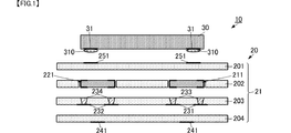
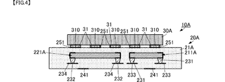
20,20A:樹脂回路基板
21,21A:積層体
30,30A:第1部品
31:端子導体
201,202,203,204:樹脂層
211,212,221,222,211A,221A:第2部品
231,232:層間接続導体
231,232:導体パターン
241:外部接続導体
251:実装用ランド導体
310:金属バンプ
320:異方性導電膜
Claims (6)
- 熱可塑性を有する複数の樹脂層が積層されてなる積層体と、
前記積層体の表面に形成され、第1部品の端子導体が接合される複数の実装用ランド導体と、
前記積層体内に配置された、前記樹脂層よりも弾性率の高い複数の第2部品と、
を備え、
前記複数の第2部品は、前記複数の樹脂層のうちの一部の樹脂層に設けられた複数の孔にそれぞれ直接的に収容されており、
前記積層体を平面視して、前記複数の第2部品は、前記複数の第2部品を結ぶ直線が前記第1部品の重心を通り、且つ、前記複数の実装用ランド導体にそれぞれ重なるように、配置されており、
前記複数の第2部品は、層間接続導体によって、前記積層体の回路導体に接続されており、
前記第2部品に直接的に接続される前記層間接続導体は、前記第2部品に対して、前記実装用ランド導体側に形成されておらず、前記実装用ランド導体と反対側に形成されている、
樹脂回路基板。 - 前記複数の第2部品は、前記積層体の高さ方向における略同じ位置に配置されている、
請求項1に記載の樹脂回路基板。 - 前記複数の第2部品は、前記積層体の裏面よりも表面に近い位置に配置されている、
請求項1または請求項2に記載の樹脂回路基板。 - 前記複数の第2部品は、前記積層体を構成する複数の樹脂層における表面側から2層目の樹脂層に配置されている、
請求項1乃至請求項3のいずれかに記載の樹脂回路基板。 - 熱可塑性を有する複数の樹脂層が積層されてなる積層体と、
前記積層体の表面に形成された複数の実装用ランド導体と、
端子導体が前記実装用ランド導体に実装された第1部品と、
前記積層体内に配置された、前記樹脂層よりも弾性率の高い複数の第2部品と、
を備え、
前記複数の第2部品は、前記複数の樹脂層のうちの一部の樹脂層に設けられた複数の孔にそれぞれ直接的に収容されており、
前記積層体を平面視して、前記複数の第2部品は、前記複数の第2部品を結ぶ直線が前記第1部品の重心を通り、且つ、前記複数の実装用ランド導体にそれぞれ重なるように、配置されており、
前記複数の第2部品は、層間接続導体によって、前記積層体の回路導体に接続されており、
前記第2部品に直接的に接続される前記層間接続導体は、前記第2部品に対して、前記実装用ランド導体側に形成されておらず、前記実装用ランド導体と反対側に形成されており、
前記端子導体は、超音波接合部、または、異方性導電部を介して、前記実装用ランド導体に接続されている、
部品搭載樹脂回路基板。 - 前記第1部品は、高周波ICであり、
前記第2部品は、前記第1部品に電気的に接続するコンデンサである、
請求項5に記載の部品搭載樹脂回路基板。
Applications Claiming Priority (3)
| Application Number | Priority Date | Filing Date | Title |
|---|---|---|---|
| JP2015172613 | 2015-09-02 | ||
| JP2015172613 | 2015-09-02 | ||
| PCT/JP2016/075265 WO2017038791A1 (ja) | 2015-09-02 | 2016-08-30 | 樹脂回路基板、部品搭載樹脂回路基板 |
Publications (2)
| Publication Number | Publication Date |
|---|---|
| JPWO2017038791A1 JPWO2017038791A1 (ja) | 2018-03-01 |
| JP6477894B2 true JP6477894B2 (ja) | 2019-03-06 |
Family
ID=58187473
Family Applications (1)
| Application Number | Title | Priority Date | Filing Date |
|---|---|---|---|
| JP2017538032A Active JP6477894B2 (ja) | 2015-09-02 | 2016-08-30 | 樹脂回路基板、部品搭載樹脂回路基板 |
Country Status (4)
| Country | Link |
|---|---|
| US (1) | US10278289B2 (ja) |
| JP (1) | JP6477894B2 (ja) |
| CN (1) | CN208016129U (ja) |
| WO (1) | WO2017038791A1 (ja) |
Families Citing this family (1)
| Publication number | Priority date | Publication date | Assignee | Title |
|---|---|---|---|---|
| GB2581149B (en) * | 2019-02-05 | 2021-11-10 | Pragmatic Printing Ltd | Flexible interposer |
Family Cites Families (14)
| Publication number | Priority date | Publication date | Assignee | Title |
|---|---|---|---|---|
| JP4610067B2 (ja) * | 2000-09-27 | 2011-01-12 | 京セラ株式会社 | 電気素子内蔵型配線基板の製造方法 |
| US6512182B2 (en) * | 2001-03-12 | 2003-01-28 | Ngk Spark Plug Co., Ltd. | Wiring circuit board and method for producing same |
| JP3910387B2 (ja) | 2001-08-24 | 2007-04-25 | 新光電気工業株式会社 | 半導体パッケージ及びその製造方法並びに半導体装置 |
| JP4492233B2 (ja) | 2003-11-27 | 2010-06-30 | 株式会社デンソー | 半導体チップの実装構造および半導体チップの実装方法 |
| JP4489485B2 (ja) * | 2004-03-31 | 2010-06-23 | 株式会社ルネサステクノロジ | 半導体装置 |
| JP3909772B2 (ja) | 2004-10-19 | 2007-04-25 | 日本アビオニクス株式会社 | 半導体実装方法およびフレキシブル配線板 |
| JP2007027255A (ja) * | 2005-07-13 | 2007-02-01 | Fujitsu Ltd | 半導体実装基板及びその製造方法 |
| JP5020671B2 (ja) * | 2007-03-27 | 2012-09-05 | 日本特殊陶業株式会社 | コンデンサ内蔵配線基板 |
| JP5240293B2 (ja) * | 2009-04-02 | 2013-07-17 | 株式会社村田製作所 | 回路基板 |
| WO2011121993A1 (ja) * | 2010-03-30 | 2011-10-06 | 株式会社村田製作所 | 部品集合体 |
| GB2497478B (en) * | 2010-10-08 | 2015-01-28 | Murata Manufacturing Co | Substrate with built-in component, and method the same |
| CN204231766U (zh) * | 2012-06-14 | 2015-03-25 | 株式会社村田制作所 | 高频模块 |
| WO2014148133A1 (ja) * | 2013-03-19 | 2014-09-25 | 株式会社村田製作所 | 積層セラミックコンデンサ |
| KR102175723B1 (ko) * | 2014-02-25 | 2020-11-09 | 삼성전자주식회사 | 반도체 패키지 |
-
2016
- 2016-08-30 CN CN201690001117.4U patent/CN208016129U/zh active Active
- 2016-08-30 JP JP2017538032A patent/JP6477894B2/ja active Active
- 2016-08-30 WO PCT/JP2016/075265 patent/WO2017038791A1/ja not_active Ceased
-
2018
- 2018-02-23 US US15/903,064 patent/US10278289B2/en active Active
Also Published As
| Publication number | Publication date |
|---|---|
| WO2017038791A1 (ja) | 2017-03-09 |
| US10278289B2 (en) | 2019-04-30 |
| US20180182680A1 (en) | 2018-06-28 |
| CN208016129U (zh) | 2018-10-26 |
| JPWO2017038791A1 (ja) | 2018-03-01 |
Similar Documents
| Publication | Publication Date | Title |
|---|---|---|
| JP5660263B1 (ja) | 電子部品、電子部品の製造方法、および、回路基板 | |
| JP6809544B2 (ja) | 電子機器 | |
| JP4046088B2 (ja) | 立体的電子回路装置およびその中継基板と中継枠 | |
| JP6160308B2 (ja) | 積層基板 | |
| CN108307584B (zh) | 元器件模块 | |
| JP6365794B2 (ja) | 樹脂多層基板、および、電子機器 | |
| WO2008050521A1 (en) | 3d electronic circuit device | |
| JP6233524B2 (ja) | 部品内蔵基板 | |
| WO2017183394A1 (ja) | 多層基板および電子機器 | |
| CN206879237U (zh) | 层叠模块用基板以及层叠模块 | |
| JP6477894B2 (ja) | 樹脂回路基板、部品搭載樹脂回路基板 | |
| JP2019040903A (ja) | 回路基板及び半導体モジュール | |
| JP6593448B2 (ja) | 樹脂基板、部品実装樹脂基板、および、部品実装樹脂基板の製造方法 | |
| JP6593447B2 (ja) | 樹脂基板、部品実装樹脂基板、樹脂基板の製造方法、部品実装樹脂基板の製造方法 | |
| JP6323622B2 (ja) | 部品実装基板 | |
| JP6890575B2 (ja) | 部品実装樹脂基板 | |
| JP6089557B2 (ja) | 電子部品モジュール | |
| JP6191808B1 (ja) | 多層基板および電子機器 | |
| JP2017204490A (ja) | 部品実装基板、および、部品実装基板の製造方法 | |
| JP2012004154A (ja) | 部品内蔵多層配線板およびその製造方法 | |
| JP2011187785A (ja) | 電子回路モジュール |
Legal Events
| Date | Code | Title | Description |
|---|---|---|---|
| A521 | Request for written amendment filed |
Free format text: JAPANESE INTERMEDIATE CODE: A523 Effective date: 20171115 |
|
| A621 | Written request for application examination |
Free format text: JAPANESE INTERMEDIATE CODE: A621 Effective date: 20171115 |
|
| A131 | Notification of reasons for refusal |
Free format text: JAPANESE INTERMEDIATE CODE: A131 Effective date: 20180925 |
|
| A521 | Request for written amendment filed |
Free format text: JAPANESE INTERMEDIATE CODE: A523 Effective date: 20181115 |
|
| TRDD | Decision of grant or rejection written | ||
| A01 | Written decision to grant a patent or to grant a registration (utility model) |
Free format text: JAPANESE INTERMEDIATE CODE: A01 Effective date: 20190108 |
|
| A61 | First payment of annual fees (during grant procedure) |
Free format text: JAPANESE INTERMEDIATE CODE: A61 Effective date: 20190121 |
|
| R150 | Certificate of patent or registration of utility model |
Ref document number: 6477894 Country of ref document: JP Free format text: JAPANESE INTERMEDIATE CODE: R150 |