JP6524929B2 - Power converter - Google Patents

Power converter Download PDF

Info

Publication number
JP6524929B2
JP6524929B2 JP2016013530A JP2016013530A JP6524929B2 JP 6524929 B2 JP6524929 B2 JP 6524929B2 JP 2016013530 A JP2016013530 A JP 2016013530A JP 2016013530 A JP2016013530 A JP 2016013530A JP 6524929 B2 JP6524929 B2 JP 6524929B2
Authority
JP
Japan
Prior art keywords
circuit
voltage
abnormality
fet
switching
Prior art date
Legal status (The legal status is an assumption and is not a legal conclusion. Google has not performed a legal analysis and makes no representation as to the accuracy of the status listed.)
Active
Application number
JP2016013530A
Other languages
Japanese (ja)
Other versions
JP2017135850A (en
Inventor
冬樹 前原
冬樹 前原
英則 小野
英則 小野
Current Assignee (The listed assignees may be inaccurate. Google has not performed a legal analysis and makes no representation or warranty as to the accuracy of the list.)
Denso Corp
Original Assignee
Denso Corp
Priority date (The priority date is an assumption and is not a legal conclusion. Google has not performed a legal analysis and makes no representation as to the accuracy of the date listed.)
Filing date
Publication date
Application filed by Denso Corp filed Critical Denso Corp
Priority to JP2016013530A priority Critical patent/JP6524929B2/en
Priority to DE102017101387.3A priority patent/DE102017101387A1/en
Publication of JP2017135850A publication Critical patent/JP2017135850A/en
Application granted granted Critical
Publication of JP6524929B2 publication Critical patent/JP6524929B2/en
Active legal-status Critical Current
Anticipated expiration legal-status Critical

Links

Images

Classifications

    • HELECTRICITY
    • H03ELECTRONIC CIRCUITRY
    • H03KPULSE TECHNIQUE
    • H03K17/00Electronic switching or gating, i.e. not by contact-making and –breaking
    • H03K17/08Modifications for protecting switching circuit against overcurrent or overvoltage
    • H03K17/081Modifications for protecting switching circuit against overcurrent or overvoltage without feedback from the output circuit to the control circuit
    • H03K17/0812Modifications for protecting switching circuit against overcurrent or overvoltage without feedback from the output circuit to the control circuit by measures taken in the control circuit
    • H03K17/08122Modifications for protecting switching circuit against overcurrent or overvoltage without feedback from the output circuit to the control circuit by measures taken in the control circuit in field-effect transistor switches
    • HELECTRICITY
    • H03ELECTRONIC CIRCUITRY
    • H03KPULSE TECHNIQUE
    • H03K17/00Electronic switching or gating, i.e. not by contact-making and –breaking
    • H03K17/08Modifications for protecting switching circuit against overcurrent or overvoltage
    • H03K2017/0806Modifications for protecting switching circuit against overcurrent or overvoltage against excessive temperature

Landscapes

  • Inverter Devices (AREA)

Description

本発明は、スイッチング素子と、スイッチング素子に関連する異常を検出する異常検出回路と、異常検出回路が異常を検出した場合、スイッチング素子を保護する保護回路とを備えた電力変換装置に関する。   The present invention relates to a power converter including a switching element, an abnormality detection circuit that detects an abnormality related to the switching element, and a protection circuit that protects the switching element when the abnormality detection circuit detects an abnormality.

従来、スイッチング素子と、スイッチング素子に関連する異常を検出する異常検出回路と、異常検出回路が異常を検出した場合、スイッチング素子を保護する保護回路とを備えた電力変換装置として、以下に示す特許文献1に開示されているモータ制御装置や、特許文献2に開示されている電力変換装置がある。   Conventionally, as a power conversion device provided with a switching element, an abnormality detection circuit that detects an abnormality related to the switching element, and a protection circuit that protects the switching element when the abnormality detection circuit detects an abnormality, There are a motor control device disclosed in Document 1 and a power conversion device disclosed in Patent Document 2.

特許文献1に開示されているモータ制御装置は、スイッチング素子と、短絡検出回路と、ドライバ部とを備えている。短絡検出回路は、スイッチング素子の短絡を検出する回路である。短絡検出回路は、スイッチング素子とは別に設けられ、配線を介してスイッチング素子に接続されている。ドライバ部は、スイッチング素子を駆動する回路である。ドライバ部は、スイッチング素子や短絡検出回路とは別に設けられ、配線を介してスイッチング素子や短絡検出回路に接続されている。ドライブ部は、スイッチング素子が正常である場合、制御信号に基づいてスイッチング素子をスイッチングさせる。一方、短絡検出回路がスイッチング素子の短絡を検出した場合、スイッチング素子をオフ状態にして、スイッチング素子を保護する。ここで、短絡検出回路が異常検出回路に、ドライバ部が保護回路に相当する。   The motor control device disclosed in Patent Document 1 includes a switching element, a short circuit detection circuit, and a driver unit. The short circuit detection circuit is a circuit that detects a short circuit of the switching element. The short circuit detection circuit is provided separately from the switching element, and is connected to the switching element through a wire. The driver unit is a circuit that drives the switching element. The driver unit is provided separately from the switching element and the short circuit detection circuit, and is connected to the switching element and the short circuit detection circuit through a wire. The drive unit switches the switching element based on the control signal when the switching element is normal. On the other hand, when the short circuit detection circuit detects a short circuit of the switching element, the switching element is turned off to protect the switching element. Here, the short circuit detection circuit corresponds to the abnormality detection circuit, and the driver unit corresponds to the protection circuit.

特許文献2に開示されている電力変換装置は、パワーMOSFETと、電圧検出回路と、制御回路とを備えている。電圧検出回路は、パワーMOSFETによって構成される電力変換回路の直流端子間の電圧を検出する回路である。電圧検出回路は、パワーMOSFETとは別に設けられ、配線を介してパワーMOSFETに接続されている。制御回路は、パワーMOSFETを駆動する回路である。制御回路は、パワーMOSFETや電圧検出回路とは別に設けられ、配線を介してパワーMOSFETや電圧検出回路に接続されている。制御回路は、電圧検出回路の検出結果に基づいてパワーMOSFETの短絡の有無を判断する。そして、パワーMOSFETが正常であると判断した場合、スイッチング素子を所定のタイミングでスイッチングさせる。一方、パワーMOSFETが短絡していると判断した場合、パワーMOSFETをオフ状態にして、パワーMOSFETを保護する。ここで、パワーMOSFETがスイッチング素子に、電圧検出回路及び制御回路が異常検出回路に、制御回路が保護回路に相当する。   The power converter disclosed in Patent Document 2 includes a power MOSFET, a voltage detection circuit, and a control circuit. The voltage detection circuit is a circuit that detects a voltage between DC terminals of a power conversion circuit configured by a power MOSFET. The voltage detection circuit is provided separately from the power MOSFET and is connected to the power MOSFET through a wire. The control circuit is a circuit that drives the power MOSFET. The control circuit is provided separately from the power MOSFET and the voltage detection circuit, and is connected to the power MOSFET and the voltage detection circuit through a wire. The control circuit determines the presence or absence of a short circuit of the power MOSFET based on the detection result of the voltage detection circuit. When it is determined that the power MOSFET is normal, the switching element is switched at a predetermined timing. On the other hand, when it is determined that the power MOSFET is short circuited, the power MOSFET is turned off to protect the power MOSFET. Here, the power MOSFET corresponds to a switching element, the voltage detection circuit and the control circuit correspond to an abnormality detection circuit, and the control circuit corresponds to a protection circuit.

特開2013−118777号公報JP, 2013-118777, A 特開2010−141990号公報JP, 2010-141990, A

前述した電力変換装置では、異常検出回路がスイッチング素子とは別に設けられ、配線を介してスイッチング素子に接続されている。また、保護回路もスイッチング素子や異常検出回路とは別に設けられ、配線を介してスイッチング素子や異常検出回路に接続されている。そのため、配線の抵抗等の影響によって異常検出回路の検出結果に誤差が生じる可能性がある。誤差が大きい場合、異常を誤検出してしまう恐れがある。また、配線の影響によって検出結果や制御信号の伝達に遅れが生じる可能性がある。遅れが大きい場合、スイッチング素子を保護しきれない恐れがある。   In the power converter described above, the abnormality detection circuit is provided separately from the switching element, and is connected to the switching element via a wire. Further, the protection circuit is also provided separately from the switching element and the abnormality detection circuit, and is connected to the switching element and the abnormality detection circuit through a wire. Therefore, an error may occur in the detection result of the abnormality detection circuit due to the influence of the resistance of the wiring or the like. If the error is large, there is a risk that an abnormality may be erroneously detected. In addition, the influence of the wiring may cause a delay in the transmission of the detection result and the control signal. If the delay is large, there is a risk that the switching element can not be protected.

本発明はこのような事情に鑑みてなされたものであり、スイッチング素子に関連する異常を正確に検出でき、スイッチング素子を速やかに保護することができる電力変換装置を提供することを目的とする。   The present invention has been made in view of such circumstances, and it is an object of the present invention to provide a power conversion device capable of accurately detecting an abnormality associated with a switching element and rapidly protecting the switching element.

上記課題を解決するためになされた請求項1に記載された本発明は、複数のスイッチング素子を備えたスイッチング回路を少なくとも1つ有する半導体モジュールと、半導体モジュール内に一体的に設けられ、スイッチング素子に関連する異常を検出する少なくとも1つの異常検出回路と、半導体モジュール内に一体的に設けられ、半導体モジュール内で異常検出回路及びスイッチング回路に接続され、異常検出回路が異常を検出した場合、スイッチング素子を保護する少なくとも1つの保護回路と、スイッチング素子に接続され、スイッチング素子を駆動する第1プリドライバと、第1プリドライバに接続され、第1プリドライバを介してスイッチング素子をスイッチングさせる制御回路と、を有し、保護回路は、スイッチング素子に接続され、スイッチング素子をオフ状態にする、第1プリドライバとは別の第2プリドライバを有し、第2プリドライバを介してスイッチング素子を保護する。この構成によれば、異常検出回路が、異常検出対象であるスイッチング素子の近傍に設けられることになる。また、保護回路が、異常検出回路や、保護対象であるスイッチング素子の近傍に設けられることになる。そのため、従来問題となっていた配線の抵抗等の影響による検出結果の誤差を抑えることができる。また、配線の影響による検出結果や制御信号の伝達遅れを抑えることができる。従って、スイッチング素子に関連する異常を正確に検出でき、スイッチング素子を速やかに保護することができる。 The present invention according to claim 1 made to solve the above problems is a semiconductor module having at least one switching circuit having a plurality of switching elements, and a switching element integrally provided in the semiconductor module And at least one anomaly detection circuit for detecting an anomaly associated with the semiconductor module, integrally provided in the semiconductor module, connected to the anomaly detection circuit and the switching circuit in the semiconductor module, and switching when the anomaly detection circuit detects an anomaly A control circuit that is connected to at least one protection circuit that protects an element, a first predriver that is connected to a switching element and drives the switching element, and is connected to a first predriver and that switches the switching element via the first predriver If, you have a protection circuit, connected to the switching element It is, to turn off the switching element, the first pre-driver has a different second pre-driver, to protect the switching element through the second pre-driver. According to this configuration, the abnormality detection circuit is provided in the vicinity of the switching element to be detected as an abnormality. In addition, a protection circuit is provided in the vicinity of the abnormality detection circuit and the switching element to be protected. Therefore, it is possible to suppress the error of the detection result due to the influence of the resistance of the wiring and the like which has conventionally been a problem. In addition, it is possible to suppress the transmission delay of the detection result and the control signal due to the influence of the wiring. Therefore, the abnormality associated with the switching element can be accurately detected, and the switching element can be protected quickly.

請求項2に記載された発明は、保護回路は、異常検出回路が異常を検出した場合、スイッチング回路のスイッチング素子を全てオフ状態にする。異常が発生した状態でスイッチング素子をオン状態にしておくと、大電流が流れてスイッチング素子が破損する可能性がある。しかし、この構成によれば、異常を検出した場合、スイッチング素子を全てオフ状態にする。そのため、スイッチング素子を確実に保護することができる。   In the invention described in claim 2, when the abnormality detection circuit detects an abnormality, the protection circuit turns off all the switching elements of the switching circuit. If the switching element is turned on in the abnormal state, a large current may flow to damage the switching element. However, according to this configuration, when an abnormality is detected, all the switching elements are turned off. Therefore, the switching element can be reliably protected.

請求項3に記載された発明は、保護回路は、スイッチング素子をオフ状態にする際のターンオフ時間が制御回路に比べて長い。異常が発生した場合、オン状態であるスイッチング素子に大電流が流れる可能性がある。大電流が流れているスイッチング素子をオフ状態にする場合、正常時に比べサージ電圧が大きくなる。そのため、サージ電圧によってスイッチング素子が破損する可能性がある。しかし、この構成によれば、保護回路は、スイッチング素子のターンオフ時間が制御回路より長い。つまり、異常時におけるスイッチング素子のターンオフ時間が、正常時におけるスイッチング素子のターンオフ時間より長い。そのため、異常時において大電流が流れているスイッチング素子をオフ状態にする場合であっても、サージ電圧を抑えることができる。従って、サージ電圧によるスイッチング素子の破損を抑えることができる。 According to the invention described in claim 3 , in the protection circuit , the turn-off time when the switching element is turned off is longer than that of the control circuit. When an abnormality occurs, a large current may flow to the switching element in the on state. When the switching element in which a large current is flowing is turned off, the surge voltage is larger than that in the normal state. Therefore, the switching element may be damaged by the surge voltage. However, according to this configuration, the protection circuit has a longer turn-off time of the switching element than the control circuit. That is, the turn-off time of the switching element at the abnormal time is longer than the turn-off time of the switching element at the normal time. Therefore, the surge voltage can be suppressed even when the switching element in which a large current flows at the time of abnormality is turned off. Therefore, damage to the switching element due to the surge voltage can be suppressed.

請求項4に記載された発明は、制御回路は、保護回路に接続され、必要に応じて保護回路を介してスイッチング素子をオフ状態にする。この構成によれば、異常検出回路以外で異常を検出した場合であっても、制御回路及び保護回路を介してスイッチング素子を速やかに保護することができる。   In the invention described in claim 4, the control circuit is connected to the protection circuit, and turns off the switching element through the protection circuit as needed. According to this configuration, even when an abnormality is detected other than the abnormality detection circuit, the switching element can be rapidly protected via the control circuit and the protection circuit.

請求項5に記載された発明は、異常検出回路は、オフ状態になるようにスイッチング素子を制御しているにも係わらず当該スイッチング素子の端子間電圧がオフ状態端子間電圧閾値以下である場合、異常であると判断する。この構成によれば、スイッチング素子の短絡故障を確実に検出することができる。   According to the fifth aspect of the present invention, in the case where the abnormality detection circuit controls the switching element so as to be in the OFF state, the inter-terminal voltage of the switching element is equal to or less than the OFF-state inter-terminal voltage threshold. Judge that it is abnormal. According to this configuration, a short circuit failure of the switching element can be reliably detected.

請求項6に記載された発明は、異常検出回路は、オン状態になるようにスイッチング素子を制御しているにも係わらず当該スイッチング素子の端子間電圧がオン状態端子間電圧閾値を超えている場合、異常であると判断する。この構成によれば、スイッチング素子のオン抵抗異常を確実に検出することができる。   In the invention described in claim 6, although the abnormality detection circuit controls the switching element to be in the on state, the inter-terminal voltage of the switching element exceeds the on-state inter-terminal voltage threshold. If it is determined that it is abnormal. According to this configuration, it is possible to reliably detect the on-resistance abnormality of the switching element.

請求項7に記載された発明は、スイッチング回路は、相補的にスイッチングされる直列接続された2つのスイッチング素子を有し、異常検出回路は、スイッチング回路の2つのスイッチング素子の制御端子電圧がともにオン状態になるような所定電圧である場合、異常であると判断する。この構成によれば、スイッチング素子の制御異常を確実に検出することができる。   The invention described in claim 7 is that the switching circuit has two switching elements connected in series that are complementarily switched, and the abnormality detection circuit is configured such that the control terminal voltages of the two switching elements of the switching circuit are both If it is a predetermined voltage that turns on, it is determined that there is an abnormality. According to this configuration, control abnormality of the switching element can be reliably detected.

請求項8に記載された発明は、異常検出回路は、スイッチング素子の温度が温度閾値を超えている場合、異常であると判断する。この構成によれば、スイッチング素子の温度異常を確実に検出することができる。   According to the eighth aspect of the present invention, the abnormality detection circuit determines that the abnormality occurs when the temperature of the switching element exceeds the temperature threshold. According to this configuration, it is possible to reliably detect the temperature abnormality of the switching element.

請求項9に記載された発明は、半導体モジュール内に一体的に設けられ、スイッチング素子の温度に応じて端子間電圧が変化する感温ダイオードを有し、異常検出回路は、感温ダイオードの端子間電圧が温度閾値に対応した所定電圧以下である場合、異常であると判断する。この構成によれば、感温ダイオードが、半導体モジュール内に一体的に設けられている。そのため、温度検出対象であるスイッチング素子の近傍に設けられることになる。従って、スイッチング素子の温度を正確に検出することができる。また、スイッチング素子の温度を検出する温度センサを別途設ける必要がない。そのため、部品点数を削減することができる。   The invention described in claim 9 includes a temperature sensitive diode which is integrally provided in the semiconductor module and in which the voltage between the terminals changes in accordance with the temperature of the switching element, and the abnormality detection circuit is a terminal of the temperature sensitive diode. If the voltage between them is equal to or less than the predetermined voltage corresponding to the temperature threshold value, it is determined that the abnormality is present. According to this configuration, the temperature sensing diode is integrally provided in the semiconductor module. Therefore, it is provided in the vicinity of the switching element which is a temperature detection target. Therefore, the temperature of the switching element can be accurately detected. In addition, it is not necessary to separately provide a temperature sensor that detects the temperature of the switching element. Therefore, the number of parts can be reduced.

請求項10に記載された発明は、半導体モジュールは、複数のスイッチング回路を有し、異常検出回路及び保護回路は、それぞれスイッチング回路の数より少ない所定数設けられている。この構成によれば、スイッチング回路に対して異常検出回路及び保護回路の数を減らすことができる。そのため、半導体モジュール内における異常検出回路及び保護回路の占める領域の増加を抑えることができる。従って、異常検出回路及び保護回路が一体的に設けられた半導体モジュールを小型化することができる。   The semiconductor module may have a plurality of switching circuits, and the abnormality detection circuits and the protection circuits may be provided in a predetermined number smaller than the number of switching circuits. According to this configuration, the number of abnormality detection circuits and protection circuits can be reduced with respect to the switching circuit. Therefore, the increase in the area occupied by the abnormality detection circuit and the protection circuit in the semiconductor module can be suppressed. Therefore, the semiconductor module in which the abnormality detection circuit and the protection circuit are integrally provided can be miniaturized.

請求項11に記載された発明は、半導体モジュールは、2つのスイッチング回路を有し、異常検出回路及び保護回路は、それぞれ1つ設けられている。この構成によれば、半導体モジュールは、2つのスイッチング回路を備えている。そして、2つのスイッチング回路の異常を検出する1つの異常検出回路と、2つのスイッチング回路を保護する1つの保護回路が、半導体モジュール内に一体的に設けられている。そのため、スイッチング回路の数が異なるさまざまな電力変換装置に広く適用することができる。つまり、異常検出回路及び保護回路が一体的に設けられた汎用性の高い半導体モジュールを構成することができる。   According to the invention described in claim 11, the semiconductor module has two switching circuits, and one abnormality detection circuit and one protection circuit are provided. According to this configuration, the semiconductor module includes two switching circuits. And one abnormality detection circuit which detects abnormality of two switching circuits, and one protection circuit which protects two switching circuits are integrally provided in the semiconductor module. Therefore, the present invention can be widely applied to various power conversion devices having different numbers of switching circuits. That is, a highly versatile semiconductor module in which the abnormality detection circuit and the protection circuit are integrally provided can be configured.

実施形態における制御装置一体型回転電機の回路図である。It is a circuit diagram of a controller integrated type rotary electric machine in an embodiment. 図1に示す第1の半導体モジュールの回路図である。It is a circuit diagram of the 1st semiconductor module shown in FIG. 図2に示す保護IC内の第1異常検出部の回路図である。It is a circuit diagram of the 1st abnormality detection part in protection IC shown in FIG. 図2に示す保護IC内の第2異常検出部の回路図である。FIG. 5 is a circuit diagram of a second abnormality detection unit in the protection IC shown in FIG. 2; 図2に示す保護IC内の第3異常検出部の回路図である。It is a circuit diagram of the 3rd abnormality detection part in protection IC shown in FIG. 図2に示す保護IC内の第4異常検出部の回路図である。It is a circuit diagram of the 4th abnormality detection part in protection IC shown in FIG. 図2に示す保護IC内の第5異常検出部の回路図である。It is a circuit diagram of the 5th abnormality detection part in protection IC shown in FIG. 図2に示す保護IC内の保護回路の回路図である。FIG. 3 is a circuit diagram of a protection circuit in the protection IC shown in FIG. 図1に示す第2の半導体モジュールの回路図である。It is a circuit diagram of the 2nd semiconductor module shown in FIG. 図1に示す第3の半導体モジュールの回路図である。It is a circuit diagram of the 3rd semiconductor module shown in FIG. 図3に示す第1異常検出部の動作を説明するためのタイムチャートである。It is a time chart for demonstrating the operation | movement of the 1st abnormality detection part shown in FIG. 図3に示す第1異常検出部の動作を説明するための別のタイムチャートである。It is another time chart for demonstrating the operation | movement of the 1st abnormality detection part shown in FIG. 図5に示す第3異常検出部の動作を説明するためのタイムチャートである。It is a time chart for demonstrating the operation | movement of the 3rd abnormality detection part shown in FIG. 図7に示す第5異常検出部の動作を説明するためのタイムチャートである。It is a time chart for demonstrating the operation | movement of the 5th abnormality detection part shown in FIG. 図8に示す保護回路の動作を説明するためのタイムチャートである。It is a time chart for demonstrating the operation | movement of the protective circuit shown in FIG.

次に、実施形態を挙げ、本発明をより詳しく説明する。本実施形態では、本発明に係る電力変換装置を、車両に搭載される制御装置一体型回転電機に適用した例を示す。   Next, the present invention will be described in more detail by way of embodiments. In this embodiment, an example is shown in which the power conversion device according to the present invention is applied to a control device integrated type rotating electrical machine mounted on a vehicle.

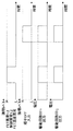
図1〜図10を参照して実施形態の制御装置一体型回転電機の構成について説明する。   The configuration of a controller-integrated electric rotating machine according to the embodiment will be described with reference to FIGS. 1 to 10.

図1に示す制御装置一体型回転電機1は、車両に搭載され、バッテリBATから電力が供給されることで、車両を駆動するための駆動力を発生する装置である。また、車両のエンジンから駆動力が供給されることで、バッテリBATを充電するための電力を発生する装置でもある。制御装置一体型回転電機1は、回転電機2と、制御装置3とを備えている。ここで、制御装置3が本発明の電力変換装置に相当する。   The controller-integrated electric rotating machine 1 shown in FIG. 1 is a device mounted on a vehicle and generating power for driving the vehicle by being supplied with electric power from a battery BAT. It is also a device that generates power for charging the battery BAT by being supplied with driving power from the engine of the vehicle. The controller integrated rotary electric machine 1 includes a rotary electric machine 2 and a controller 3. Here, the control device 3 corresponds to the power conversion device of the present invention.

回転電機2は、バッテリBATから電力が供給されることで、車両を駆動するための駆動力を発生する機器である。また、エンジンから駆動力が供給されることで、バッテリBATを充電するための電力を発生する機器でもある。回転電機2は、固定子20と、回転子21と、回転角度検出装置22とを備えている。   The rotating electrical machine 2 is a device that generates a driving force for driving a vehicle by being supplied with electric power from the battery BAT. It is also a device that generates power for charging the battery BAT by being supplied with driving power from the engine. The rotary electric machine 2 includes a stator 20, a rotor 21, and a rotation angle detection device 22.

固定子20は、磁路の一部を構成するとともに、電流が流れることで回転磁界を発生する部材である。また、磁路の一部を構成するとともに、回転子21の発生する磁束と鎖交することで交流を発生する部材でもある。固定子20は、固定子巻線200、201を備えている。固定子巻線200は、U相巻線200a、V相巻線200b及びW相巻線200cをY結線して構成されている。固定子巻線201は、U相巻線201a、V相巻線201b及びW相巻線201cをY結線して構成されている。U相巻線200a、201a、V相巻線200b、201b及びW相巻線200c、201cは、制御装置3にそれぞれ接続されている。   The stator 20 is a member that forms a part of a magnetic path and generates a rotating magnetic field when a current flows. Moreover, while forming a part of magnetic path, it is also a member which generate | occur | produces alternating current by linking with the magnetic flux which the rotor 21 generate | occur | produces. The stator 20 includes stator windings 200 and 201. The stator winding 200 is configured by Y-connecting the U-phase winding 200a, the V-phase winding 200b, and the W-phase winding 200c. The stator winding 201 is configured by Y-connecting the U-phase winding 201a, the V-phase winding 201b, and the W-phase winding 201c. U-phase windings 200a and 201a, V-phase windings 200b and 201b, and W-phase windings 200c and 201c are connected to control device 3, respectively.

回転子21は、磁路の一部を構成するとともに、電流が流れることで磁極を形成する部材である。回転子21は、界磁巻線210を備えている。界磁巻線210は、制御装置3に接続されている。   The rotor 21 is a member that forms a part of a magnetic path and forms a magnetic pole by the flow of current. The rotor 21 includes a field winding 210. The field winding 210 is connected to the controller 3.

回転角度検出装置22は、回転子21の回転角度を検出装置である。回転角度検出装置22は、制御装置3に接続されている。   The rotation angle detection device 22 is a detection device of the rotation angle of the rotor 21. The rotation angle detection device 22 is connected to the control device 3.

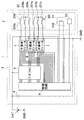
制御装置3は、回転電機2に駆動力を発生させるために、バッテリBATから回転電機2に供給される電力を制御する装置である。また、バッテリBATを充電するために、回転電機2の発生した電力を変換してバッテリBATに供給する装置でもある。制御装置3は、平滑コンデンサ4と、半導体モジュール5〜7と、プリドライバ8と、制御回路9とを備えている。   The control device 3 is a device that controls the power supplied from the battery BAT to the rotating electrical machine 2 in order to cause the rotating electrical machine 2 to generate a driving force. In addition, in order to charge the battery BAT, it is also a device that converts the power generated by the rotating electrical machine 2 and supplies the converted power to the battery BAT. The control device 3 includes a smoothing capacitor 4, semiconductor modules 5 to 7, a predriver 8, and a control circuit 9.

平滑コンデンサ4は、バッテリBATから供給される直流を平滑化するための素子である。平滑コンデンサ4の一端は、バッテリBATの正極端に接続されている。また、他端は、バッテリBATの負極端が接続される電位基準点であるグランドGNDに接続されている。具体的には、車体に接続されている。   The smoothing capacitor 4 is an element for smoothing direct current supplied from the battery BAT. One end of the smoothing capacitor 4 is connected to the positive end of the battery BAT. The other end is connected to ground GND which is a potential reference point to which the negative end of battery BAT is connected. Specifically, it is connected to the vehicle body.

半導体モジュール5〜7は、制御回路9によって制御され、バッテリBATから供給される直流を3相交流に変換して固定子巻線200、201に供給するモジュールである。また、固定子巻線200、201の発生する3相交流を直流に変換してバッテリBATに供給するモジュールでもある。具体的には、半導体モジュール5と半導体モジュール6の一部が、バッテリBATから供給される直流を3相交流に変換して固定子巻線200に供給する。また、固定子巻線200の発生する3相交流を直流に変換してバッテリBATに供給する。半導体モジュール6の一部と半導体モジュール7が、バッテリBATから供給される直流を3相交流に変換して固定子巻線201に供給する。また、固定子巻線201の発生する3相交流を直流に変換してバッテリBATに供給する。   The semiconductor modules 5 to 7 are modules controlled by the control circuit 9 to convert direct current supplied from the battery BAT into three-phase alternating current and to supply the stator windings 200 and 201 with the direct current. It is also a module that converts the three-phase alternating current generated by the stator windings 200 and 201 into direct current and supplies the direct current to the battery BAT. Specifically, the semiconductor module 5 and a part of the semiconductor module 6 convert the direct current supplied from the battery BAT into a three-phase alternating current and supply it to the stator winding 200. Further, the three-phase alternating current generated by the stator winding 200 is converted into direct current and supplied to the battery BAT. A part of the semiconductor module 6 and the semiconductor module 7 convert the direct current supplied from the battery BAT into a three-phase alternating current and supply it to the stator winding 201. Further, the three-phase alternating current generated by the stator winding 201 is converted into direct current and supplied to the battery BAT.

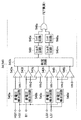
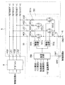
図2に示すように、半導体モジュール5は、スイッチング回路50、51と、感温ダイオード520〜523と、保護IC53とを備えている。   As shown in FIG. 2, the semiconductor module 5 includes switching circuits 50 and 51, temperature sensitive diodes 520 to 523, and a protection IC 53.

スイッチング回路50は、制御回路9によって制御され、スイッチングすることでバッテリから供給される直流を交流に変換してU相巻線200aに供給する回路である。また、U相巻線200aから供給される交流を直流に変換してバッテリBATに供給する回路である。スイッチング回路50は、FET500、501と、抵抗502とを備えている。FET500、501は、スイッチングすることで直流を交流に変換するスイッチング素子である。抵抗502は電流を検出するための素子である。FET500、501はドレイン−ソース間にダイオードを備えている。FET500、501は直列接続されている。FET500のソースがFET501のドレインに接続されている。FET500のドレインは、バッテリBATに接続される半導体モジュール5の端子Bに接続されている。FET501のソースは、抵抗502を介して、グランドGNDに接続される半導体モジュール5の端子Gに接続されている。抵抗502のFET501側の一端は、制御回路9に接続される半導体モジュール5の端子S1+、及び、保護IC53の端子LS1にそれぞれ接続されている。抵抗502の端子G側の他端は、制御回路9に接続される半導体モジュール5の端子S1−に接続されている。FET500、501の直列接続点は、U相巻線200aに接続される半導体モジュール5の端子P1に接続されている。   The switching circuit 50 is a circuit which is controlled by the control circuit 9 and is switched to convert direct current supplied from the battery into alternating current and supply it to the U-phase winding 200a. In addition, it is a circuit that converts alternating current supplied from the U-phase winding 200a into direct current and supplies it to the battery BAT. The switching circuit 50 includes FETs 500 and 501 and a resistor 502. The FETs 500 and 501 are switching elements that convert direct current into alternating current by switching. The resistor 502 is an element for detecting a current. The FETs 500 and 501 have a diode between the drain and the source. The FETs 500 and 501 are connected in series. The source of the FET 500 is connected to the drain of the FET 501. The drain of the FET 500 is connected to the terminal B of the semiconductor module 5 connected to the battery BAT. The source of the FET 501 is connected via the resistor 502 to the terminal G of the semiconductor module 5 connected to the ground GND. One end of the resistor 502 on the FET 501 side is connected to the terminal S1 + of the semiconductor module 5 connected to the control circuit 9 and the terminal LS1 of the protection IC 53. The other end of the resistor 502 on the terminal G side is connected to the terminal S1− of the semiconductor module 5 connected to the control circuit 9. The series connection point of the FETs 500 and 501 is connected to the terminal P1 of the semiconductor module 5 connected to the U-phase winding 200a.

スイッチング回路50は、FET500、501を所定のタイミングで相補的にスイッチングすることで、バッテリBATから供給される直流を交流に変換してU相巻線200aに供給する。また、FET500、501のダイオードによってU相巻線200aから供給される交流を直流に変換してバッテリBATに供給する。   The switching circuit 50 complementarily switches the FETs 500 and 501 at a predetermined timing to convert direct current supplied from the battery BAT into alternating current and supply it to the U-phase winding 200 a. Further, the alternating current supplied from the U-phase winding 200a by the diodes of the FETs 500 and 501 is converted into a direct current and supplied to the battery BAT.

スイッチング回路51は、制御回路9によって制御され、スイッチングすることでバッテリから供給される直流を交流に変換してV相巻線200bに供給する回路である。また、V相巻線200bから供給される交流を直流に変換してバッテリBATに供給する回路である。スイッチング回路51は、FET510、511と、抵抗512とを備えている。FET510、511は、スイッチングすることで直流を交流に変換するスイッチング素子である。抵抗512は電流を検出するための素子である。FET510、511はドレイン−ソース間にダイオードを備えている。FET510、511は直列接続されている。FET510のソースがFET511のドレインに接続されている。FET510のドレインは、バッテリBATに接続される半導体モジュール5の端子Bに接続されている。FET501のソースは、抵抗512を介して、グランドGNDに接続される半導体モジュール5の端子Gに接続されている。抵抗512のFET511側の一端は、制御回路9に接続される半導体モジュール5の端子S2+、及び、保護IC53の端子LS2にそれぞれ接続されている。抵抗512の端子G側の他端は、制御回路9に接続される半導体モジュール5の端子S2−に接続されている。FET510、511の直列接続点は、V相巻線200bに接続される半導体モジュール5の端子P2に接続されている。   The switching circuit 51 is a circuit which is controlled by the control circuit 9 and is switched to convert direct current supplied from the battery into alternating current and supply it to the V-phase winding 200b. In addition, it is a circuit that converts alternating current supplied from the V-phase winding 200b into direct current and supplies the direct current to the battery BAT. The switching circuit 51 includes FETs 510 and 511 and a resistor 512. The FETs 510 and 511 are switching elements that convert direct current into alternating current by switching. The resistor 512 is an element for detecting a current. The FETs 510 and 511 have a diode between the drain and the source. The FETs 510 and 511 are connected in series. The source of the FET 510 is connected to the drain of the FET 511. The drain of the FET 510 is connected to the terminal B of the semiconductor module 5 connected to the battery BAT. The source of the FET 501 is connected via the resistor 512 to the terminal G of the semiconductor module 5 connected to the ground GND. One end of the resistor 512 on the side of the FET 511 is connected to the terminal S2 + of the semiconductor module 5 connected to the control circuit 9 and the terminal LS2 of the protection IC 53. The other end on the terminal G side of the resistor 512 is connected to the terminal S2− of the semiconductor module 5 connected to the control circuit 9. The series connection point of the FETs 510 and 511 is connected to the terminal P2 of the semiconductor module 5 connected to the V-phase winding 200b.

スイッチング回路51は、FET510、511を所定のタイミングで相補的にスイッチングすることで、バッテリBATから供給される直流を交流に変換してV相巻線200bに供給する。また、FET510、511のダイオードによってV相巻線200bから供給される交流を直流に変換してバッテリBATに供給する。   The switching circuit 51 complementarily switches the FETs 510 and 511 at a predetermined timing to convert direct current supplied from the battery BAT into alternating current and supply the alternating current to the V-phase winding 200 b. Further, the alternating current supplied from the V-phase winding 200b by the diodes of the FETs 510 and 511 is converted into a direct current and supplied to the battery BAT.

感温ダイオード520〜523は、FET500、501、510、511の温度をそれぞれ検出するための素子である。具体的には、定電流を流すことで温度に応じた電圧を出力する素子である。より具体的には、温度上昇に伴って電圧が低下する素子である。感温ダイオード520〜523は、それぞれ直列接続され、保護IC53にそれぞれ接続されている。   The temperature sensitive diodes 520 to 523 are elements for detecting the temperatures of the FETs 500, 501, 510, and 511, respectively. Specifically, it is an element that outputs a voltage according to temperature by flowing a constant current. More specifically, it is an element whose voltage decreases as the temperature rises. The temperature sensitive diodes 520 to 523 are connected in series and connected to the protection IC 53, respectively.

保護IC53は、半導体モジュール5内に一体的に設けられ、FET500、501、510、511に関連する異常を検出し、FET500、501、510、511を保護する素子である。保護IC53は、図3〜図7に示す異常検出回路54と、図8に示す保護回路55とを備えている。   The protection IC 53 is an element that is integrally provided in the semiconductor module 5, detects an abnormality related to the FETs 500, 501, 510, 511, and protects the FETs 500, 501, 510, 511. The protection IC 53 includes an abnormality detection circuit 54 shown in FIGS. 3 to 7 and a protection circuit 55 shown in FIG.

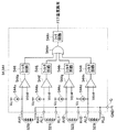
図3〜図7に示す異常検出回路54は、FET500、501、510、511に関連する異常を検出する回路である。異常検出回路54は、第1〜第5異常検出部540〜544を備えている。   The abnormality detection circuit 54 illustrated in FIGS. 3 to 7 is a circuit that detects an abnormality associated with the FETs 500, 501, 510, and 511. The abnormality detection circuit 54 includes first to fifth abnormality detection units 540 to 544.

図3に示す第1異常検出部540は、FET500、501の異常を検出するブロックである。具体的には、FET500、501の短絡及びオン抵抗異常を検出するブロックである。第1異常検出部540は、差電圧検出回路540a〜540dと、コンパレータ540e〜540jと、判定回路540k、フィルタ回路540l、540mと、ラッチ回路540n、540oと、OR回路540pとを備えている。   The first abnormality detection unit 540 illustrated in FIG. 3 is a block that detects an abnormality of the FETs 500 and 501. Specifically, it is a block that detects a short circuit and an on-resistance abnormality of the FETs 500 and 501. The first abnormality detection unit 540 includes differential voltage detection circuits 540a to 540d, comparators 540e to 540j, determination circuits 540k, filter circuits 540l and 540m, latch circuits 540n and 540o, and an OR circuit 540p.

差電圧検出回路540aは、FET500のゲート電圧とソース電圧から、それらの差電圧であるゲート−ソース間電圧Vgsを検出し出力する回路である。ここで、FETのゲート−ソース間電圧Vgsが本発明のスイッチング素子の制御端子電圧に相当する。差電圧検出回路540aの一方の入力端はFET500のゲートに接続される保護IC53の端子HG1に、他方の入力端はFET500のソースに接続される保護IC53の端子HS1にそれぞれ接続されている。   The difference voltage detection circuit 540 a is a circuit that detects and outputs a gate-source voltage Vgs which is a difference voltage between the gate voltage and the source voltage of the FET 500. Here, the gate-source voltage Vgs of the FET corresponds to the control terminal voltage of the switching element of the present invention. One input end of the differential voltage detection circuit 540a is connected to the terminal HG1 of the protection IC 53 connected to the gate of the FET 500, and the other input end is connected to the terminal HS1 of the protection IC 53 connected to the source of the FET 500.

差電圧検出回路540bは、FET500のドレイン電圧とソース電圧から、それらの差電圧であるドレイン−ソース間電圧Vdsを検出し出力する回路である。ここで、FETのドレイン−ソース間電圧Vdsが本発明のスイッチング素子の端子間電圧に相当する。差電圧検出回路540bの一方の入力端はFET500のドレインに接続される保護IC53の端子B1に、他方の入力端はFET500のソースに接続される保護IC53の端子HS1にそれぞれ接続されている。   The difference voltage detection circuit 540 b is a circuit that detects and outputs a drain-source voltage Vds that is a difference voltage between the drain voltage and the source voltage of the FET 500. Here, the drain-to-source voltage Vds of the FET corresponds to the terminal-to-terminal voltage of the switching element of the present invention. One input end of the differential voltage detection circuit 540b is connected to the terminal B1 of the protection IC 53 connected to the drain of the FET 500, and the other input end is connected to the terminal HS1 of the protection IC 53 connected to the source of the FET 500.

差電圧検出回路540cは、FET501のゲート電圧とソース電圧から、それらの差電圧であるゲート−ソース間電圧Vgsを検出し出力する回路である。差電圧検出回路540cの一方の入力端はFET501のゲートに接続される保護IC53の端子LG1に、他方の入力端はFET501のソースに接続される保護IC53の端子LS1にそれぞれ接続されている。   The difference voltage detection circuit 540 c is a circuit that detects and outputs a gate-source voltage Vgs which is a difference voltage between the gate voltage and the source voltage of the FET 501. One input end of the differential voltage detection circuit 540c is connected to the terminal LG1 of the protection IC 53 connected to the gate of the FET 501, and the other input end is connected to the terminal LS1 of the protection IC 53 connected to the source of the FET 501.

差電圧検出回路540dは、FET501のドレイン電圧とソース電圧から、それらの差電圧であるドレイン−ソース間電圧Vdsを検出し出力する回路である。差電圧検出回路540dの一方の入力端はFET501のドレインに接続される保護IC53の端子HS1に、他方の入力端はFET501のソースに接続される保護IC53の端子LS1にそれぞれ接続されている。   The difference voltage detection circuit 540 d is a circuit that detects and outputs a drain-source voltage Vds which is a difference voltage between the drain voltage and the source voltage of the FET 501. One input end of the differential voltage detection circuit 540d is connected to the terminal HS1 of the protection IC 53 connected to the drain of the FET 501, and the other input end is connected to the terminal LS1 of the protection IC 53 connected to the source of the FET 501.

コンパレータ540eは、差電圧検出回路540aの出力するFET500のゲート−ソース間電圧Vgsを電圧閾値Vth1と比較し、比較結果を出力する素子である。FETは、ゲート−ソース間電圧Vgsによってオン状態になるように制御されているかオフ状態になるように制御されているかが決まる。電圧閾値Vth1は、FETのゲート−ソース間電圧Vgsに基づいてオン状態になるように制御されているかオフ状態になるように制御されているかを判断できる所定電圧に設定されている。コンパレータ540eは、FET500がオン状態になるように制御されている場合、ゲート−ソース間電圧Vgsが電圧閾値Vth1より大きくなり、出力電圧がハイレベルHになる。一方、FET500がオフ状態になるように制御されている場合、ゲート−ソース間電圧Vgsが電圧閾値Vth1より小さくなり、出力電圧がローレベルLになる。コンパレータ540eの非反転入力端は差電圧検出回路540aの出力端に、反転入力端は電圧閾値Vth1に設定された基準電源にそれぞれ接続されている。   The comparator 540 e is an element that compares the gate-source voltage Vgs of the FET 500 output from the difference voltage detection circuit 540 a with the voltage threshold Vth1 and outputs the comparison result. The FET is controlled by the gate-source voltage Vgs to be turned on or off. The voltage threshold value Vth1 is set to a predetermined voltage that can determine whether it is controlled to be in the on state or controlled to be in the off state based on the gate-source voltage Vgs of the FET. In the comparator 540e, when the FET 500 is controlled to be turned on, the gate-source voltage Vgs becomes larger than the voltage threshold Vth1, and the output voltage becomes high level H. On the other hand, when the FET 500 is controlled to be turned off, the gate-source voltage Vgs becomes smaller than the voltage threshold Vth1, and the output voltage becomes low level L. The non-inverted input end of the comparator 540e is connected to the output end of the differential voltage detection circuit 540a, and the inverted input end is connected to the reference power supply set to the voltage threshold Vth1.

コンパレータ540fは、差電圧検出回路540bの出力するFET500のドレイン−ソース間電圧Vdsを電圧閾値Vth2と比較し、比較結果を出力する素子である。FETは、オン状態の場合とオフ状態の場合でドレイン−ソース間電圧Vdsが変化する。電圧閾値Vth2は、FETのドレイン−ソース間電圧Vdsに基づいてオン状態であるかオフ状態であるかを判断できる所定電圧に設定されている。ここで、電圧閾値Vth2が本発明のオフ状態端子間電圧閾値に相当する。コンパレータ540fは、FET500がオン状態である場合、ドレイン−ソース間電圧Vdsが電圧閾値Vth2より小さくなり、出力電圧がローレベルLになる。一方、FET500がオフ状態である場合、ドレイン−ソース間電圧Vdsが電圧閾値Vth2より大きくなり、出力電圧がハイレベルHになる。コンパレータ540fの非反転入力端は差電圧検出回路540bの出力端に、反転入力端は電圧閾値Vth2に設定された基準電源にそれぞれ接続されている。   The comparator 540 f is an element that compares the drain-source voltage Vds of the FET 500 output from the difference voltage detection circuit 540 b with the voltage threshold Vth2 and outputs the comparison result. In the FET, the drain-source voltage Vds changes in the on state and the off state. The voltage threshold Vth2 is set to a predetermined voltage that can determine whether the on state or the off state is based on the drain-source voltage Vds of the FET. Here, the voltage threshold Vth2 corresponds to the off-state inter-terminal voltage threshold of the present invention. In the comparator 540f, when the FET 500 is in the on state, the drain-source voltage Vds becomes smaller than the voltage threshold Vth2, and the output voltage becomes low level L. On the other hand, when the FET 500 is in the off state, the drain-source voltage Vds becomes larger than the voltage threshold Vth2, and the output voltage becomes high level H. The non-inverted input end of the comparator 540f is connected to the output end of the differential voltage detection circuit 540b, and the inverted input end is connected to the reference power supply set to the voltage threshold Vth2.

コンパレータ540gは、差電圧検出回路540bの出力するFET500のドレイン−ソース間電圧Vdsを電圧閾値Vth3と比較し、比較結果を出力する素子である。FETは、オン状態である場合、ドレイン−ソース間に所定のオン抵抗を有する。このとき、電流が流れることで、ドレイン−ソース間電圧Vdsが、オン抵抗と流れる電流に応じた所定電圧になる。FETの異常に伴ってオン抵抗が増加した場合、ドレイン−ソース間電圧Vdsが大きくなる。電圧閾値Vth3は、FETのドレイン−ソース間電圧Vdsに基づいてオン抵抗が増加したことを判断できる所定電圧に設定されている。ここで、電圧閾値Vth3が本発明のオン状態端子間電圧閾値に相当する。コンパレータ540gは、FET500のドレイン−ソース間電圧Vdsが電圧閾値Vth3より大きい場合、出力電圧がハイレベルHになる。一方、FET500のドレイン−ソース間電圧Vdsが電圧閾値Vth3より以下である場合、出力電圧がローレベルLになる。コンパレータ540gの非反転入力端は差電圧検出回路540bの出力端に、反転入力端は電圧閾値Vth3に設定された基準電源にそれぞれ接続されている。   The comparator 540g is an element that compares the drain-source voltage Vds of the FET 500 output from the difference voltage detection circuit 540b with the voltage threshold Vth3 and outputs the comparison result. When the FET is in the on state, it has a predetermined on resistance between the drain and the source. At this time, when the current flows, the drain-source voltage Vds becomes a predetermined voltage according to the on resistance and the current flowing. If the on-resistance increases with the abnormality of the FET, the drain-source voltage Vds increases. The voltage threshold value Vth3 is set to a predetermined voltage that can determine that the on-resistance has increased based on the drain-source voltage Vds of the FET. Here, the voltage threshold Vth3 corresponds to the on-state inter-terminal voltage threshold of the present invention. In the comparator 540g, when the drain-source voltage Vds of the FET 500 is larger than the voltage threshold Vth3, the output voltage becomes high level H. On the other hand, when the drain-source voltage Vds of the FET 500 is less than or equal to the voltage threshold Vth3, the output voltage becomes low level L. The non-inverted input terminal of the comparator 540g is connected to the output terminal of the differential voltage detection circuit 540b, and the inverted input terminal is connected to the reference power supply set to the voltage threshold Vth3.

コンパレータ540hは、差電圧検出回路540cの出力するFET501のゲート−ソース間電圧Vgsを電圧閾値Vth1と比較し、比較結果を出力する素子である。コンパレータ540hは、FET501がオン状態になるように制御されている場合、ゲート−ソース間電圧Vgsが電圧閾値Vth1より大きくなり、出力電圧がハイレベルHになる。一方、FET501がオフ状態になるように制御されている場合、ゲート−ソース間電圧Vgsが電圧閾値Vth1より小さくなり、出力電圧がローレベルLになる。コンパレータ540hの非反転入力端は差電圧検出回路540cの出力端に、反転入力端は電圧閾値Vth1に設定された基準電源にそれぞれ接続されている。   The comparator 540h is an element that compares the gate-source voltage Vgs of the FET 501 output from the difference voltage detection circuit 540c with the voltage threshold Vth1 and outputs the comparison result. In the comparator 540h, when the FET 501 is controlled to be turned on, the gate-source voltage Vgs becomes larger than the voltage threshold Vth1, and the output voltage becomes high level H. On the other hand, when the FET 501 is controlled to be in the OFF state, the gate-source voltage Vgs becomes smaller than the voltage threshold Vth1, and the output voltage becomes low level L. The non-inverted input terminal of the comparator 540h is connected to the output terminal of the differential voltage detection circuit 540c, and the inverted input terminal is connected to the reference power supply set to the voltage threshold Vth1.

コンパレータ540iは、差電圧検出回路540dの出力するFET501のドレイン−ソース間電圧Vdsを電圧閾値Vth2と比較し、比較結果を出力する素子である。コンパレータ540iは、FET501がオン状態である場合、ドレイン−ソース間電圧Vdsが電圧閾値Vth2より小さくなり、出力電圧がローレベルLになる。一方、FET501がオフ状態である場合、ドレイン−ソース間電圧Vdsが電圧閾値Vth2より大きくなり、出力電圧がハイレベルHになる。コンパレータ540iの非反転入力端は差電圧検出回路540dの出力端に、反転入力端は電圧閾値Vth2に設定された基準電源にそれぞれ接続されている。   The comparator 540i is an element that compares the drain-source voltage Vds of the FET 501 output from the difference voltage detection circuit 540d with the voltage threshold Vth2, and outputs the comparison result. In the comparator 540i, when the FET 501 is in the on state, the drain-source voltage Vds becomes smaller than the voltage threshold Vth2, and the output voltage becomes low level L. On the other hand, when the FET 501 is in the OFF state, the drain-source voltage Vds becomes larger than the voltage threshold Vth2, and the output voltage becomes high level H. The non-inverted input end of the comparator 540i is connected to the output end of the differential voltage detection circuit 540d, and the inverted input end is connected to the reference power supply set to the voltage threshold Vth2.

コンパレータ540jは、差電圧検出回路540dの出力するFET501のドレイン−ソース間電圧Vdsを電圧閾値Vth3と比較し、比較結果を出力する素子である。コンパレータ540jは、FET501のドレイン−ソース間電圧Vdsが電圧閾値Vth3より大きい場合、出力電圧がハイレベルHになる。一方、FET501のドレイン−ソース間電圧Vdsが電圧閾値Vth3より以下である場合、出力電圧がローレベルLになる。コンパレータ540jの非反転入力端は差電圧検出回路540dの出力端に、反転入力端は電圧閾値Vth3の基準電源にそれぞれ接続されている。   The comparator 540 j is an element that compares the drain-source voltage Vds of the FET 501 output from the difference voltage detection circuit 540 d with the voltage threshold Vth3 and outputs the comparison result. The output voltage of the comparator 540 j is high when the drain-source voltage Vds of the FET 501 is larger than the voltage threshold Vth3. On the other hand, when the drain-source voltage Vds of the FET 501 is less than or equal to the voltage threshold Vth3, the output voltage becomes low level L. The non-inverting input terminal of the comparator 540j is connected to the output terminal of the differential voltage detection circuit 540d, and the inverting input terminal is connected to the reference power supply of the voltage threshold Vth3.

判定回路540kは、コンパレータ540e、540fの出力に基づいてFET500が短絡しているか否か、及び、コンパレータ540h、540iの出力に基づいてFET501が短絡しているか否かを判定する回路である。コンパレータ540e、540gの出力に基づいてFET500のオン抵抗が異常であるか否か、及び、コンパレータ540h、540jの出力に基づいてFET501のオン抵抗が異常であるか否かを判定する回路でもある。判定回路540kは、コンパレータ540eの出力電圧が、FET500がオフ状態になるように制御されていることを示すローレベルLであるにも係わらず、コンパレータ540fの出力電圧が、FET500がオン状態であることを示すローレベルLである場合、FET500が短絡していると判定する。コンパレータ540hの出力電圧が、FET501がオフ状態になるように制御されていることを示すローレベルLであるにも係わらず、コンパレータ540iの出力電圧が、FET501がオン状態であることを示すローレベルLである場合、FET501が短絡していると判定する。そして、FET500、501に少なくともいずれかが短絡していると判定した場合、一方の出力の論理レベルがハイレベルHになる。また、コンパレータ540eの出力電圧が、FET500がオン状態になるように制御されていることを示すハイレベルHであるにも係わらず、コンパレータ540gの出力電圧が、ドレイン−ソース間電圧Vdsが大きいことを示すハイレベルHである場合、FET500のオン抵抗が異常であると判定する。コンパレータ540hの出力電圧が、FET501がオン状態になるように制御されていることを示すハイレベルHであるにも係わらず、コンパレータ540jの出力電圧が、ドレイン−ソース間電圧Vdsが大きいことを示すハイレベルHである場合、FET501のオン抵抗が異常であると判定する。そして、FET500、501に少なくともいずれかのオン抵抗が異常であると判定した場合、他方の出力の論理レベルがハイレベルHになる。判定回路540kの入力端はコンパレータ540e〜540jの出力端にそれぞれ接続されている。   The determination circuit 540k is a circuit that determines whether the FET 500 is shorted based on the outputs of the comparators 540e and 540f and whether the FET 501 is shorted based on the outputs of the comparators 540h and 540i. It is also a circuit that determines whether the on resistance of the FET 500 is abnormal based on the outputs of the comparators 540e and 540g, and whether the on resistance of the FET 501 is abnormal based on the outputs of the comparators 540h and 540j. In the determination circuit 540k, although the output voltage of the comparator 540e is at the low level L indicating that the FET 500 is controlled to be in the off state, the output voltage of the comparator 540f is in the on state. When it is low level L which shows that, it determines with FET500 having shorted. Although the output voltage of the comparator 540h is low level L indicating that the FET 501 is controlled to be turned off, the output voltage of the comparator 540i is low level indicating that the FET 501 is turned on. If it is L, it is determined that the FET 501 is shorted. When it is determined that at least one of the FETs 500 and 501 is shorted, the logic level of one of the outputs becomes high level H. Further, although the output voltage of the comparator 540e is at the high level H indicating that the FET 500 is controlled to be turned on, the output voltage of the comparator 540g has a large drain-source voltage Vds. If the on-resistance of the FET 500 is abnormal, it is determined that the on-resistance of the FET 500 is abnormal. The output voltage of the comparator 540j indicates that the drain-source voltage Vds is large although the output voltage of the comparator 540h is high level H indicating that the FET 501 is controlled to be turned on. When the H level is high, it is determined that the on resistance of the FET 501 is abnormal. When it is determined that at least one of the on resistances of the FETs 500 and 501 is abnormal, the logic level of the other output becomes high level H. The input ends of the determination circuit 540k are connected to the output ends of the comparators 540e to 540j, respectively.

フィルタ回路540l、540mは、判定回路540kの出力に含まれるノイズを除去し、所定の処理時間経過後に出力する回路である。具体的には、デジタルフィルタである。フィルタ回路540lの入力端は判定回路540kの一方の出力端に、フィルタ回路540mの入力端は判定回路540kの他方の出力端にそれぞれ接続されている。   The filter circuits 540l and 540m are circuits that remove noise included in the output of the determination circuit 540k and output the result after a predetermined processing time has elapsed. Specifically, it is a digital filter. The input end of the filter circuit 540l is connected to one output end of the determination circuit 540k, and the input end of the filter circuit 540m is connected to the other output end of the determination circuit 540k.

ラッチ回路540n、540oは、フィルタ回路540l、540mによってノイズが除去された判定回路540kの出力を所定のホールド時間保持する回路である。ラッチ回路540nは、判定回路540kの出力の論理レベルがFET500、501の少なくともいずれかが短絡していると判定したことを示すハイレベルHである場合、フィルタ回路540lの処理時間経過後に、所定のホールド時間、出力の論理レベルがハイレベルHになる。ラッチ回路540oは、判定回路540kの出力の論理レベルがFET500、501の少なくともいずれかのオン抵抗が異常であると判定したことを示すハイレベルHである場合、フィルタ回路540mの処理時間経過後に、所定のホールド時間、出力の倫理レベルがハイレベルHになる。ラッチ回路540nの入力端はフィルタ回路540lの出力端に、ラッチ回路540oの入力端はフィルタ回路540mの出力端にそれぞれ接続されている。   The latch circuits 540n and 540o are circuits that hold the output of the determination circuit 540k from which noise has been removed by the filter circuits 540l and 540m for a predetermined hold time. When the logic level of the output of determination circuit 540k is high level H indicating that at least one of FETs 500 and 501 is determined to be short circuited, a predetermined time is set after the processing time of filter circuit 540l. The hold time, the logic level of the output becomes high level H. When the logic level of the output of determination circuit 540k is high level H indicating that the ON resistance of at least one of FETs 500 and 501 is abnormal, latch circuit 540o passes after the processing time of filter circuit 540m elapses. The predetermined hold time, the output ethics level becomes high level H. The input end of the latch circuit 540n is connected to the output end of the filter circuit 5401, and the input end of the latch circuit 540o is connected to the output end of the filter circuit 540m.

OR回路540pは、ラッチ回路540n、540oの出力の論理和を演算し、演算結果をFET異常1として出力する回路である。OR回路540pは、ラッチ回路540n、540oの少なくともいずれかの出力の論理レベルがハイレベルHである場合、出力の論理レベルがハイレベルHになる。つまり、FET500、501の短絡及びオン抵抗異常を検出した場合、出力の論理レベルがハイレベルHになる。OR回路540pの一方の入力端はラッチ回路540nの出力端に、他方の入力端はラッチ回路540oの出力端にそれぞれ接続されている。   The OR circuit 540 p is a circuit that calculates the logical sum of the outputs of the latch circuits 540 n and 540 o and outputs the calculation result as the FET abnormality 1. In the OR circuit 540p, when the logic level of at least one of the outputs of the latch circuits 540n and 540o is high level H, the logic level of the output becomes high level H. That is, when the short circuit and the on-resistance abnormality of the FETs 500 and 501 are detected, the logic level of the output becomes the high level H. One input end of the OR circuit 540p is connected to the output end of the latch circuit 540n, and the other input end is connected to the output end of the latch circuit 540o.

図4に示す第2異常検出部541は、FET510、511の異常を検出するブロックである。具体的には、FET510、511の短絡及びオン抵抗異常を検出するブロックである。第2異常検出部541は、差電圧検出回路541a〜541dと、コンパレータ541e〜541jと、判定回路541kと、フィルタ回路541l、541mと、ラッチ回路541n、541oと、OR回路541pとを備えている。   The second abnormality detection unit 541 illustrated in FIG. 4 is a block that detects an abnormality of the FETs 510 and 511. Specifically, it is a block that detects a short circuit of the FETs 510 and 511 and an ON resistance abnormality. The second abnormality detection unit 541 includes differential voltage detection circuits 541a to 541d, comparators 541e to 541j, a determination circuit 541k, filter circuits 541l and 541m, latch circuits 541n and 541o, and an OR circuit 541p. .

差電圧検出回路541a〜541dは、入力端の接続を除いて第1異常検出部540の差電圧検出回路540a〜540dと同一の回路である。差電圧検出回路541aの一方の入力端はFET510のゲートに接続される保護IC53の端子HG2に、他方の入力端はFET510のソースに接続される保護IC53の端子HS2にそれぞれ接続されている。差電圧検出回路541bの一方の入力端はFET510のドレインに接続される保護IC53の端子B2に、他方の入力端はFET510のソースに接続される保護IC53の端子HS2にそれぞれ接続されている。差電圧検出回路541cの一方の入力端はFET511のゲートに接続される保護IC53の端子LG2に、他方の入力端はFET511のソースに接続される保護IC53の端子LS2にそれぞれ接続されている。差電圧検出回路541dの一方の入力端はFET511のドレインに接続される保護IC53の端子HS2に、他方の入力端はFET511のソースに接続される保護IC53の端子LS2にそれぞれ接続されている。   The differential voltage detection circuits 541 a to 541 d are the same circuits as the differential voltage detection circuits 540 a to 540 d of the first abnormality detection unit 540 except for the connection of the input terminal. One input end of the differential voltage detection circuit 541 a is connected to the terminal HG 2 of the protection IC 53 connected to the gate of the FET 510, and the other input end is connected to the terminal HS 2 of the protection IC 53 connected to the source of the FET 510. One input end of the differential voltage detection circuit 541 b is connected to the terminal B 2 of the protection IC 53 connected to the drain of the FET 510, and the other input end is connected to the terminal HS 2 of the protection IC 53 connected to the source of the FET 510. One input end of the differential voltage detection circuit 541 c is connected to the terminal LG 2 of the protection IC 53 connected to the gate of the FET 511, and the other input end is connected to the terminal LS 2 of the protection IC 53 connected to the source of the FET 511. One input end of the differential voltage detection circuit 541 d is connected to the terminal HS 2 of the protection IC 53 connected to the drain of the FET 511, and the other input end is connected to the terminal LS 2 of the protection IC 53 connected to the source of the FET 511.

コンパレータ541e〜541j、判定回路541k、フィルタ回路541l、541m、ラッチ回路541n、541o及びOR回路541pは、第1異常検出部540のコンパレータ540e〜540j、判定回路540k、フィルタ回路540l、540m、ラッチ回路540n、540o及びOR回路540pと同一のものであり、同一構成である。   The comparators 541e to 541j, the determination circuits 541k, the filter circuits 541l and 541m, the latch circuits 541n and 541o, and the OR circuit 541p are the comparators 540e to 540j, the determination circuits 540k, the filter circuits 540l and 540m, and the latch circuits of the first abnormality detection unit 540. It is the same as 540 n, 540 o and the OR circuit 540 p and has the same configuration.

図5に示す第3異常検出部542は、FET500、501に対する制御異常を検出するブロックである。FET500、501は、本来相補的にスイッチングされる。第3異常検出部542は、FET500、501をともにオン状態にするような異常な制御状態を検出するブロックである。第3異常検出部542は、差電圧検出回路542a、542bと、コンパレータ542c、542dと、AND回路542eと、フィルタ回路542fと、ラッチ回路542gとを備えている。   The third abnormality detection unit 542 illustrated in FIG. 5 is a block that detects a control abnormality with respect to the FETs 500 and 501. The FETs 500 and 501 are inherently switched complementarily. The third abnormality detection unit 542 is a block that detects an abnormal control state in which the FETs 500 and 501 are both turned on. The third abnormality detection unit 542 includes differential voltage detection circuits 542 a and 542 b, comparators 542 c and 542 d, an AND circuit 542 e, a filter circuit 542 f, and a latch circuit 542 g.

差電圧検出回路542aは、FET500のゲート電圧とソース電圧から、それらの差電圧であるゲート−ソース間電圧Vgsを検出し出力する回路である。差電圧検出回路542aの一方の入力端は保護IC53の端子HG1に、他方の入力端は保護IC53の端子HS1にそれぞれ接続されている。   The differential voltage detection circuit 542a is a circuit that detects and outputs a gate-source voltage Vgs which is a differential voltage between the gate voltage and the source voltage of the FET 500. One input end of the differential voltage detection circuit 542a is connected to the terminal HG1 of the protection IC 53, and the other input end is connected to the terminal HS1 of the protection IC 53.

差電圧検出回路542bは、FET501のゲート電圧とソース電圧から、それらの差電圧であるゲート−ソース間電圧Vgsを検出し出力する回路である。差電圧検出回路542bの一方の入力端は保護IC53の端子LG1に、他方の入力端は保護IC53の端子LS1にそれぞれ接続されている。   The difference voltage detection circuit 542 b is a circuit that detects and outputs a gate-source voltage Vgs which is a difference voltage between the gate voltage and the source voltage of the FET 501. One input end of the differential voltage detection circuit 542 b is connected to the terminal LG 1 of the protection IC 53, and the other input end is connected to the terminal LS 1 of the protection IC 53.

コンパレータ542cは、差電圧検出回路542aの出力するFET500のゲート−ソース間電圧Vgsを電圧閾値Vth1と比較し、比較結果を出力する素子である。コンパレータ542cは、FET500がオン状態になるように制御されている場合、ゲート−ソース間電圧Vgsが電圧閾値Vth1より大きくなり、出力電圧がハイレベルHになる。一方、FET500がオフ状態になるように制御されている場合、ゲート−ソース間電圧Vgsが電圧閾値Vth1より小さくなり、出力電圧がローレベルLになる。コンパレータ542cの非反転入力端は差電圧検出回路542aの出力端に、反転入力端は電圧閾値Vth1に設定された基準電源にそれぞれ接続されている。   The comparator 542c is an element that compares the gate-source voltage Vgs of the FET 500 output from the difference voltage detection circuit 542a with the voltage threshold Vth1 and outputs the comparison result. In the comparator 542c, when the FET 500 is controlled to be turned on, the gate-source voltage Vgs becomes larger than the voltage threshold Vth1, and the output voltage becomes high level H. On the other hand, when the FET 500 is controlled to be turned off, the gate-source voltage Vgs becomes smaller than the voltage threshold Vth1, and the output voltage becomes low level L. The non-inverted input end of the comparator 542c is connected to the output end of the differential voltage detection circuit 542a, and the inverted input end is connected to the reference power supply set to the voltage threshold Vth1.

コンパレータ542dは、差電圧検出回路542bの出力するFET501のゲート−ソース間電圧Vgsを電圧閾値Vth1と比較し、比較結果を出力する素子である。コンパレータ542dは、FET501がオン状態になるように制御されている場合、ゲート−ソース間電圧Vgsが電圧閾値Vth1より大きくなり、出力電圧がハイレベルHになる。一方、FET501がオフ状態になるように制御されている場合、ゲート−ソース間電圧Vgsが電圧閾値Vth1より小さくなり、出力電圧がローレベルLになる。コンパレータ542dの非反転入力端は差電圧検出回路542bの出力端に、反転入力端は電圧閾値Vth1に設定された基準電源にそれぞれ接続されている。   The comparator 542 d is an element that compares the gate-source voltage Vgs of the FET 501 output from the difference voltage detection circuit 542 b with the voltage threshold Vth1 and outputs the comparison result. In the comparator 542d, when the FET 501 is controlled to be in the on state, the gate-source voltage Vgs becomes larger than the voltage threshold Vth1, and the output voltage becomes high level H. On the other hand, when the FET 501 is controlled to be in the OFF state, the gate-source voltage Vgs becomes smaller than the voltage threshold Vth1, and the output voltage becomes low level L. The non-inverted input end of the comparator 542 d is connected to the output end of the differential voltage detection circuit 542 b, and the inverted input end is connected to the reference power supply set to the voltage threshold Vth1.

AND回路542eは、コンパレータ542c、542dの出力の論理積を演算し、演算結果を出力する回路である。FET500、501は、本来相補的にスイッチングされる。そのため、FET500、501が、ともにオン状態になるように制御されることはない。AND回路542eは、コンパレータ542cの出力電圧が、FET500がオン状態になるように制御されていることを示すハイレベルHであり、かつ、コンパレータ542dの出力電圧が、FET501がオン状態になるように制御されていることを示すハイレベルHである場合、FET500、501の制御が異常であると判定し、出力の論理レベルがハイレベルHになる。AND回路542eの一方の入力端はコンパレータ542cの出力端に、他方の入力端はコンパレータ542dの出力端にそれぞれ接続されている。   The AND circuit 542 e is a circuit that calculates the logical product of the outputs of the comparators 542 c and 542 d and outputs the calculation result. The FETs 500 and 501 are inherently switched complementarily. Therefore, the FETs 500 and 501 are not controlled to be turned on together. The AND circuit 542e has a high level H indicating that the output voltage of the comparator 542c is controlled to turn on the FET 500, and the output voltage of the comparator 542d causes the FET 501 to be turned on. When it is a high level H indicating that control is being performed, it is determined that the control of the FETs 500 and 501 is abnormal, and the logic level of the output becomes high level H. One input end of the AND circuit 542e is connected to the output end of the comparator 542c, and the other input end is connected to the output end of the comparator 542d.

フィルタ回路542fは、AND回路542eの出力に含まれるノイズを除去し、所定の処理時間経過後に出力する回路である。具体的には、デジタルフィルタである。フィルタ回路542fの入力端はAND回路542eの出力端に接続されている。   The filter circuit 542 f is a circuit that removes noise contained in the output of the AND circuit 542 e and outputs the noise after a predetermined processing time has elapsed. Specifically, it is a digital filter. The input end of the filter circuit 542 f is connected to the output end of the AND circuit 542 e.

ラッチ回路542gは、フィルタ回路542fによってノイズが除去されたAND回路542eの出力を所定のホールド時間保持し、制御異常1として出力する回路である。ラッチ回路542gは、AND回路542e出力の論理レベルがハイレベルHである場合、フィルタ回路542fの処理時間経過後に、所定のホールド時間、出力の論理レベルがハイレベルHになる。つまり、FET500、501をともにオン状態にするような異常な制御状態を検出した場合、出力の論理レベルがハイレベルHになる。ラッチ回路542gの入力端はフィルタ回路542fの出力端に接続されている。   The latch circuit 542 g is a circuit that holds the output of the AND circuit 542 e from which noise has been removed by the filter circuit 542 f for a predetermined hold time, and outputs it as a control abnormality 1. In the latch circuit 542g, when the logic level of the output of the AND circuit 542e is high level H, the logic level of the output becomes high level H for a predetermined hold time after the processing time of the filter circuit 542f elapses. That is, when an abnormal control state is detected to turn on both the FETs 500 and 501, the logic level of the output becomes high level H. The input end of the latch circuit 542 g is connected to the output end of the filter circuit 542 f.

図6に示す第4異常検出部543は、FET510、511に対する制御異常を検出するブロックである。FET510、511は、本来相補的にスイッチングされる。第4異常検出部543は、FET510、511をともにオン状態にするような異常な制御状態を検出するブロックである。第4異常検出部543は、差電圧検出回路543a、543bと、コンパレータ543c、543dと、AND回路543eと、フィルタ回路543fと、ラッチ回路543gとを備えている。   The fourth abnormality detection unit 543 illustrated in FIG. 6 is a block that detects a control abnormality with respect to the FETs 510 and 511. The FETs 510 and 511 are inherently switched in a complementary manner. The fourth abnormality detection unit 543 is a block that detects an abnormal control state in which the FETs 510 and 511 are both turned on. The fourth abnormality detection unit 543 includes difference voltage detection circuits 543a and 543b, comparators 543c and 543d, an AND circuit 543e, a filter circuit 543f, and a latch circuit 543g.

差電圧検出回路543a、543bは、入力端の接続を除いて第3異常検出部542の差電圧検出回路542a、542b、同一の回路である。差電圧検出回路543aの一方の入力端は保護IC53の端子HG2に、他方の入力端は保護IC53の端子HS2にそれぞれ接続されている。差電圧検出回路543bの一方の入力端は保護IC53の端子LG2に、他方の入力端は保護IC53の端子LS2にそれぞれ接続されている。   The differential voltage detection circuits 543a and 543b are the same circuits as the differential voltage detection circuits 542a and 542b of the third abnormality detection unit 542 except for the connection of the input terminal. One input end of the differential voltage detection circuit 543a is connected to the terminal HG2 of the protection IC 53, and the other input end is connected to the terminal HS2 of the protection IC 53. One input end of the differential voltage detection circuit 543 b is connected to the terminal LG 2 of the protection IC 53, and the other input end is connected to the terminal LS 2 of the protection IC 53.

コンパレータ543c、543d、AND回路543e、フィルタ回路543f及びラッチ回路543gは、第3異常検出部542のコンパレータ542c、542d、AND回路542e、フィルタ回路542f及びラッチ回路542gと同一のものであり、同一構成である。   The comparators 543c and 543d, the AND circuit 543e, the filter circuit 543f, and the latch circuit 543g are the same as the comparators 542c and 542d, the AND circuit 542e, the filter circuit 542f, and the latch circuit 542g of the third abnormality detection unit 542 and have the same configuration. It is.

図7に示す第5異常検出部544は、FET500、501、510、511の温度異常を検出ブロックである。第5異常検出部544は、定電流回路544a〜544dと、コンパレータ544e〜544hと、フィルタ回路544i〜544lと、OR回路544mと、ラッチ回路544nとを備えている。   The fifth abnormality detection unit 544 illustrated in FIG. 7 is a block that detects a temperature abnormality of the FETs 500, 501, 510, and 511. The fifth abnormality detection unit 544 includes constant current circuits 544a to 544d, comparators 544e to 544h, filter circuits 544i to 544l, an OR circuit 544m, and a latch circuit 544n.

定電流回路544a〜544dは、感温ダイオード520〜523に定電流を供給する回路である。定電流回路544a〜544dは、電圧Vcの電源に接続されている。定電流回路544a〜544dの出力端は、感温ダイオード520〜523のアノードに接続される保護IC53の端子AH1、AL1、AH2、AL2にそれぞれ接続されている。感温ダイオード520〜523のカソードに接続される保護IC53の端子KH1、KL1、KH2、KL2は、グランドGNDに接続される保護IC53の端子Gに接続されている。   The constant current circuits 544a to 544d are circuits for supplying a constant current to the temperature sensitive diodes 520 to 523. The constant current circuits 544a to 544d are connected to the power supply of the voltage Vc. The output ends of the constant current circuits 544a to 544d are connected to terminals AH1, AL1, AH2 and AL2 of the protection IC 53 connected to the anodes of the temperature sensitive diodes 520 to 523, respectively. The terminals KH1, KL1, KH2 and KL2 of the protection IC 53 connected to the cathodes of the temperature sensitive diodes 520 to 523 are connected to the terminal G of the protection IC 53 connected to the ground GND.

コンパレータ544e〜544hは、感温ダイオード520〜523の端子間電圧を電圧閾値Vth4と比較し、比較結果を出力する素子である。電圧閾値Vth4は、感温ダイオード520〜523の端子間電圧に基づいてFETが温度異常であると判断する温度閾値に対応した所定電圧に設定されている。コンパレータ544e〜544hは、FET500、501、510、511の温度が温度閾値より小さい場合、感温ダイオード520〜523の端子間電圧が電圧閾値Vth4より大きくなり、出力電圧がハイレベルHになる。一方、FET500、501、510、511の温度が温度閾値以上である場合、感温ダイオード520〜523の端子間電圧が電圧閾値Vth4以下になり、出力電圧がローレベルLになる。コンパレータ544e〜544hの非反転入力端は感温ダイオード520〜523のアノードに接続される保護IC53の端子AH1、AL1、AH2、AL2に、反転入力端は電圧閾値Vth4に設定された基準電源にそれぞれ接続されている。   The comparators 544 e to 544 h are elements that compare the voltage between the terminals of the temperature sensitive diodes 520 to 523 with the voltage threshold Vth4 and output the comparison result. The voltage threshold value Vth4 is set to a predetermined voltage corresponding to the temperature threshold value at which the FET determines that the temperature is abnormal based on the voltage between the terminals of the temperature sensitive diodes 520 to 523. In the comparators 544e to 544h, when the temperature of the FETs 500, 501, 510, and 511 is smaller than the temperature threshold, the voltage across terminals of the temperature sensitive diodes 520 to 523 becomes larger than the voltage threshold Vth4, and the output voltage becomes high level H. On the other hand, when the temperature of the FETs 500, 501, 510, and 511 is equal to or higher than the temperature threshold, the voltage between terminals of the temperature sensitive diodes 520 to 523 becomes equal to or lower than the voltage threshold Vth4, and the output voltage becomes low level L. Non-inverting input terminals of the comparators 544 e to 544 h are connected to the anodes of the temperature sensing diodes 520 to 523 to terminals AH1, AL1, AH2 and AL2 of the protective IC 53, and inverting input terminals are connected to reference power supplies set to the voltage threshold Vth4. It is connected.

フィルタ回路544i〜544lは、コンパレータ544e〜544hの出力に含まれるノイズを除去し、所定の処理時間経過後に出力する回路である。具体的には、デジタルフィルタである。フィルタ回路544i〜544lの入力端はコンパレータ544e〜544hの出力端にそれぞれ接続されている。   The filter circuits 544i to 544l are circuits that remove noise included in the outputs of the comparators 544e to 544h and output the result after a predetermined processing time has elapsed. Specifically, it is a digital filter. The input ends of the filter circuits 544i to 544l are connected to the output ends of the comparators 544e to 544h, respectively.

OR回路544mは、フィルタ回路544i〜544lによってノイズが除去されたコンパレータ544e〜544hの出力の論理和を演算し、演算結果を出力する回路である。OR回路544mは、フィルタ回路544i〜544lによってノイズが除去されたコンパレータ544e〜544hの出力の少なくともいずれかが、FETの温度が温度閾値以上であることを示すローレベルLである場合、FET500、501、510、511の少なくともいずれかの温度が異常であると判定し、出力の論理レベルがハイレベルHになる。OR回路544mの4つの入力端はフィルタ回路544i〜544lの出力端にそれぞれ接続されている。   The OR circuit 544m is a circuit that calculates the logical sum of the outputs of the comparators 544e to 544h from which noises have been removed by the filter circuits 544i to 544l, and outputs the calculation result. When at least one of the outputs of the comparators 544 e to 544 h from which noise has been removed by the filter circuits 544 i to 544 l is the low level L indicating that the temperature of the FET is equal to or higher than the temperature threshold, the OR circuit 544 m , 510, or 511, and the logic level of the output becomes high level H. The four input ends of the OR circuit 544m are connected to the output ends of the filter circuits 544i to 544l, respectively.

ラッチ回路544nは、OR回路544mの出力を所定のホールド時間保持し、FET温度異常として出力する回路である。ラッチ回路544nは、OR回路544mの出力の論理レベルがハイレベルHである場合、所定のホールド時間、出力の論理レベルがハイレベルHになる。つまり、FET500、501、510、511の温度異常を検出した場合、出力の論理レベルがハイレベルHになる。ラッチ回路544nの入力端はOR回路544mの出力端に接続されている。   The latch circuit 544 n is a circuit that holds the output of the OR circuit 544 m for a predetermined hold time and outputs it as an FET temperature abnormality. In the latch circuit 544 n, when the logic level of the output of the OR circuit 544 m is high level H, the logic level of the output becomes high level H for a predetermined hold time. That is, when the temperature abnormality of the FET 500, 501, 510, 511 is detected, the logic level of the output becomes the high level H. The input end of the latch circuit 544 n is connected to the output end of the OR circuit 544 m.

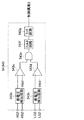
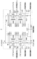
図8に示す保護回路55は、異常検出回路54が異常を検出した場合、FET500、501、510、511を全てオフ状態にして、FET500、501、510、511を保護する回路である。また、制御回路9からの指令に基づいてFET500、501、510、511を全てオフ状態にして、FET500、501、510、511を保護する回路でもある。保護回路55は、処理回路550と、プリドライバ551とを備えている。   The protection circuit 55 illustrated in FIG. 8 is a circuit that protects the FETs 500, 501, 510, and 511 by turning off all the FETs 500, 501, 510, and 511 when the abnormality detection circuit 54 detects an abnormality. It is also a circuit that protects all the FETs 500, 501, 510, and 511 by turning off all the FETs 500, 501, 510, and 511 based on a command from the control circuit 9. The protection circuit 55 includes a processing circuit 550 and a predriver 551.

処理回路550は、異常検出回路54が異常を検出した場合、FET500、501、510、511をオフ状態にするための駆動信号を出力する回路である。具体的には、FET異常1、FET異常2、制御異常1及び制御異常2の少なくともいずれかがハイレベルHである場合、FET500、501、510、511をオフ状態にするための駆動信号を出力する回路である。また、制御回路9からの指令に基づいてFET500、501、510、511をオフ状態にするための駆動信号を出力する回路でもある。処理回路550は、FETをオフ状態にする際のターンオフ時間が制御回路9に比べ長くなるように設定されている。処理回路550の入力端は、図3〜図7に示す第1〜第5異常検出部540〜544の出力端、及び、保護IC53の端子OFFにそれぞれ接続されている。具体的には、OR回路540p、541pの出力端、ラッチ回路542g、543g、544nの出力端、及び、保護IC53の端子OFFにそれぞれ接続されている。保護IC53の端子OFFは、図1に示す制御回路9に接続される半導体モジュール5の端子OFFに接続されている。   The processing circuit 550 is a circuit that outputs a drive signal for turning off the FETs 500, 501, 510, and 511 when the abnormality detection circuit 54 detects an abnormality. Specifically, when at least one of the FET abnormality 1, the FET abnormality 2, the control abnormality 1 and the control abnormality 2 is at the high level H, a drive signal for turning off the FETs 500, 501, 510, and 511 is output. Circuit. It is also a circuit that outputs a drive signal for turning off the FETs 500, 501, 510, and 511 based on a command from the control circuit 9. The processing circuit 550 is set such that the turn-off time when the FET is turned off is longer than that of the control circuit 9. The input end of the processing circuit 550 is connected to the output end of the first to fifth abnormality detection units 540 to 544 shown in FIGS. 3 to 7 and the terminal OFF of the protection IC 53. Specifically, the output terminals of the OR circuits 540p and 541p, the output terminals of the latch circuits 542g, 543g and 544n, and the terminal OFF of the protection IC 53 are connected. The terminal OFF of the protection IC 53 is connected to the terminal OFF of the semiconductor module 5 connected to the control circuit 9 shown in FIG.

図8に示すプリドライバ551は、処理回路550によって制御され、プリドライバ8の出力に関係なく、図2に示すFET500、501、510、511をオフ状態にする回路である。図8に示すように、プリドライバ551は、FET551a〜551dと、抵抗551e〜551hと、駆動回路551i、551jとを備えている。   The predriver 551 shown in FIG. 8 is a circuit which is controlled by the processing circuit 550 and turns off the FETs 500, 501, 510 and 511 shown in FIG. 2 regardless of the output of the predriver 8. As shown in FIG. 8, the predriver 551 includes FETs 551 a to 551 d, resistors 551 e to 551 h, and drive circuits 551 i and 551 j.

FET551a〜551dは、オン状態になってFET500、501、510、511のゲートをグランドGNDに接続することでゲート−ドレイン間電圧Vgsを低下させ、プリドライバ8の出力に関係なくFET500、501、510、511をオフ状態にするスイッチング素子である。抵抗551e〜551hは、FET500、501、510、511のゲートをグランドGNDに接続する際に流れる電流を制限するための素子である。FET551a〜551dのドレインは、抵抗551e〜551hを介して保護IC53の端子HG1、LG1、HG2、LG2にそれぞれ接続されている。保護IC53の端子HG1、LG1、HG2、LG2は、FET500、501、510、511のゲートに接続される半導体モジュール5の端子HG1、LG1、HG2、LG2に接続されている。FET551a〜551dのソースは保護IC53の端子Gに接続されている。保護IC53の端子Gは、グランドGNDに接続される半導体モジュール5の端子Gに接続されている。   The FETs 551a to 551d are turned on to connect the gates of the FETs 500, 501, 510, and 511 to the ground GND, thereby reducing the gate-drain voltage Vgs, and the FETs 500, 501, and 510 are independent of the output of the predriver 8. , And 511 are turned off. The resistors 551e to 551h are elements for limiting the current flowing when the gates of the FETs 500, 501, 510, and 511 are connected to the ground GND. The drains of the FETs 551a to 551d are connected to the terminals HG1, LG1, HG2, and LG2 of the protection IC 53 through the resistors 551e to 551h, respectively. The terminals HG1, LG1, HG2, LG2 of the protection IC 53 are connected to the terminals HG1, LG1, HG2, LG2 of the semiconductor module 5 connected to the gates of the FETs 500, 501, 510, 511. The sources of the FETs 551 a to 551 d are connected to the terminal G of the protection IC 53. The terminal G of the protection IC 53 is connected to the terminal G of the semiconductor module 5 connected to the ground GND.

駆動回路551i、551jは、処理回路550によって制御され、FET551a〜551dをオン状態にする回路である。駆動回路551i、551jは、処理回路550がFET500、501、510、511をオフ状態にする駆動信号を出力した場合、FET551a〜551dをオン状態にする。駆動回路551i、551jの入力端は処理回路550の出力端に、出力端はFET551a〜551dのゲートにそれぞれ接続されている。   The drive circuits 551i and 551j are circuits controlled by the processing circuit 550 to turn on the FETs 551a to 551d. The drive circuits 551i and 551j turn on the FETs 551a to 551d when the processing circuit 550 outputs a drive signal to turn off the FETs 500, 501, 510, and 511. The input ends of the drive circuits 551i and 551j are connected to the output end of the processing circuit 550, and the output ends are connected to the gates of the FETs 551a to 551d.

図9に示す半導体モジュール6は、スイッチング回路60、61と、感温ダイオード620〜623と、保護IC63とを備えている。スイッチング回路60は、FET600、601と、抵抗602とを備えている。スイッチング回路61は、FET610、611と、抵抗612とを備えている。   The semiconductor module 6 shown in FIG. 9 includes switching circuits 60 and 61, temperature sensitive diodes 620 to 623, and a protection IC 63. The switching circuit 60 includes FETs 600 and 601 and a resistor 602. The switching circuit 61 includes FETs 610 and 611 and a resistor 612.

スイッチング回路60、61は、FET600、601の直列接続点、及び、FET610、611の直列接続点の接続を除いて半導体モジュール5のスイッチング回路50、51と同一の回路である。FET600、601の直列接続点は、W相巻線200cに接続される半導体モジュール6の端子P1に接続されている。FET610、611の直列接続点は、U相巻線201aに接続される半導体モジュール6の端子P2に接続されている。感温ダイオード620〜623及び保護IC63は、半導体モジュール5の感温ダイオード520〜523及び保護IC53と同一のものであり、同一構成である。   The switching circuits 60 and 61 are the same circuits as the switching circuits 50 and 51 of the semiconductor module 5 except for the connection of the series connection point of the FETs 600 and 601 and the series connection point of the FETs 610 and 611. The series connection point of the FETs 600 and 601 is connected to the terminal P1 of the semiconductor module 6 connected to the W-phase winding 200c. The series connection point of the FETs 610 and 611 is connected to the terminal P2 of the semiconductor module 6 connected to the U-phase winding 201a. The temperature sensitive diodes 620 to 623 and the protection IC 63 are the same as the temperature sensitive diodes 520 to 523 and the protection IC 53 of the semiconductor module 5, and have the same configuration.

図10に示す半導体モジュール7は、スイッチング回路70、71と、感温ダイオード720〜723と、保護IC73とを備えている。スイッチング回路70は、FET700、701と、抵抗702とを備えている。スイッチング回路71は、FET710、711と、抵抗712とを備えている。   The semiconductor module 7 shown in FIG. 10 includes switching circuits 70 and 71, temperature sensitive diodes 720 to 723 and a protection IC 73. The switching circuit 70 includes FETs 700 and 701 and a resistor 702. The switching circuit 71 includes FETs 710 and 711, and a resistor 712.

スイッチング回路70、71は、FET700、701の直列接続点、及び、FET710、711の直列接続点の接続を除いて半導体モジュール5のスイッチング回路50、51と同一の回路である。FET700、701の直列接続点は、V相巻線201bに接続される半導体モジュール7の端子P1に接続されている。FET710、711の直列接続点は、W相巻線201cに接続される半導体モジュール7の端子P2に接続されている。感温ダイオード720〜723及び保護IC73は、半導体モジュール5の感温ダイオード520〜523及び保護IC53と同一のものであり、同一構成である。   The switching circuits 70 and 71 are the same as the switching circuits 50 and 51 of the semiconductor module 5 except for the connection of the series connection point of the FETs 700 and 701 and the series connection point of the FETs 710 and 711. The series connection point of the FETs 700 and 701 is connected to the terminal P1 of the semiconductor module 7 connected to the V-phase winding 201b. The series connection point of the FETs 710 and 711 is connected to the terminal P2 of the semiconductor module 7 connected to the W-phase winding 201c. The temperature sensing diodes 720 to 723 and the protection IC 73 are the same as the temperature sensing diodes 520 to 523 and the protection IC 53 of the semiconductor module 5, and have the same configuration.

図1に示すプリドライバ8は、制御回路9によって制御され、図2、図9及び図10に示す半導体モジュール5〜7のFET500、501、510、511、600、601、610、611、700、701、710、711を駆動する回路である。図1に示すように、プリドライバ8は、バッテリBATの正極端に接続されている。プリドライバ8の出力端は、図2、図9及び図10に示すFET500、501、510、511、600、601、610、611、700、701、710、711のゲートに接続される半導体モジュール5〜7の端子HG1、LG1、HG2、LG2にそれぞれ接続されている。   The predriver 8 shown in FIG. 1 is controlled by the control circuit 9, and the FETs 500, 501, 510, 511, 600, 601, 610, 611, 700, of the semiconductor modules 5 to 7 shown in FIGS. The circuits 701, 710, and 711 are driven. As shown in FIG. 1, the predriver 8 is connected to the positive terminal of the battery BAT. The output terminal of the predriver 8 is connected to the gates of the FETs 500, 501, 510, 511, 600, 601, 610, 611, 700, 701, 710, 711 shown in FIG. 2, FIG. 9 and FIG. The terminals HG1, LG1, HG2, and LG2 of .about.7 are respectively connected.

図1に示す制御回路9は、回転電機2に駆動力を発生させる場合、バッテリBATから界磁巻線210に供給される直流を制御するとともに、プリドライバ8を介して図2、図9及び図10に示す半導体モジュール5〜7のFET500、501、510、511、600、601、610、611、700、701、710、711をスイッチングさせることで、図1に示すバッテリBATから供給される直流を3相交流に変換して固定子巻線200、201に供給する回路である。また、バッテリBATを充電する場合、バッテリBATから界磁巻線210に供給される直流を制御するとともに、プリドライバ8を介して図2、図9及び図10に示すFET500、501、510、511、600、601、610、611、700、701、710、711をオフ状態にすることで、FETのダイオードによって図1に示す固定子巻線200、201の発生する3相交流を直流に変換してバッテリBATに供給する回路でもある。制御回路9は、回転電機2に駆動力を発生させる場合、回転角度検出装置22の検出結果、及び、図2、図9及び図10に示す半導体モジュール5〜7の抵抗502、512、602、612、702、712の検出結果に基づいてFET500、501、510、511、600、601、610、611、700、701、710、711をスイッチングさせる。   The control circuit 9 shown in FIG. 1 controls the direct current supplied from the battery BAT to the field winding 210 when the rotary electric machine 2 generates the driving force, and also via the predriver 8 in FIGS. By switching the FETs 500, 501, 510, 511, 600, 601, 610, 611, 700, 701, 710, and 711 of the semiconductor modules 5 to 7 shown in FIG. 10, the direct current supplied from the battery BAT shown in FIG. Are converted into three-phase alternating current and supplied to the stator windings 200 and 201. In addition, when charging the battery BAT, the direct current supplied from the battery BAT to the field winding 210 is controlled, and the FETs 500, 501, 510, and 511 shown in FIGS. , 600, 601, 610, 611, 700, 701, 710, and 711 are turned off, the three-phase alternating current generated by the stator windings 200 and 201 shown in FIG. It is also a circuit that supplies the battery BAT. When the control circuit 9 causes the rotating electrical machine 2 to generate a driving force, the detection result of the rotation angle detection device 22 and the resistances 502, 512, 602 of the semiconductor modules 5 to 7 shown in FIG. 2, FIG. 9 and FIG. The FETs 500, 501, 510, 511, 600, 601, 610, 611, 700, 701, 710, 711 are switched based on the detection results of 612, 702, 712.

図1に示すように、制御回路9はバッテリBATの正極端に接続されるとともに、グランドGNDを介してバッテリBATの負極端に接続されている。また、界磁巻線210に接続されている。制御回路9の入力端は回転角度検出装置22、及び、図2、図9及び図10に示す抵抗502、512、602、612、702、712に接続される半導体モジュール5〜7の端子S1+、S1−、S2+、S2−にそれぞれ接続されている。出力端はプリドライバ8の入力端に接続されている。   As shown in FIG. 1, the control circuit 9 is connected to the positive terminal of the battery BAT and is also connected to the negative terminal of the battery BAT through the ground GND. Also, it is connected to the field winding 210. The input end of the control circuit 9 is a terminal S1 + of the rotation angle detection device 22 and the semiconductor modules 5 to 7 connected to the resistors 502, 512, 602, 612, 702, 712 shown in FIGS. It is connected to S1-, S2 +, and S2- respectively. The output end is connected to the input end of the predriver 8.

図1に示す制御回路9は、必要に応じて保護回路55を介してFET500、501、510、511をオフ状態にする。具体的には、外部から入手した情報に基づいてFETの異常を検出した場合、保護回路55を介してFET500、501、510、511をオフ状態にする。より具体的には、図8に示す保護回路55の端子OFFに論理レベルがハイレベルHの信号を入力し、保護回路55を介してFET500、501、510、511をオフ状態にする。FET600、601、610、611、700、701、710、711に対しても同様である。制御回路9は、図2、図9及び図10に示す保護IC53、63、73の端子OFFに接続される半導体モジュール5〜7の端子OFFにそれぞれ接続されている。   The control circuit 9 shown in FIG. 1 turns off the FETs 500, 501, 510, and 511 via the protection circuit 55 as necessary. Specifically, when an abnormality in the FET is detected based on information obtained from the outside, the FETs 500, 501, 510, and 511 are turned off via the protection circuit 55. More specifically, a high level H signal is input to the terminal OFF of the protection circuit 55 shown in FIG. 8 to turn off the FETs 500, 501, 510, and 511 via the protection circuit 55. The same applies to the FETs 600, 601, 610, 611, 700, 701, 710, and 711. The control circuit 9 is connected to the terminals OFF of the semiconductor modules 5 to 7 connected to the terminals OFF of the protection ICs 53, 63 and 73 shown in FIG. 2, FIG. 9 and FIG.

次に、図1、図2、図9及び図10を参照して制御装置一体型回転電機の動作について説明する。まず、回転電機に車両を駆動するための駆動力を発生させる際の動作について説明する。   Next, the operation of the controller-integrated electric rotating machine will be described with reference to FIGS. 1, 2, 9 and 10. First, an operation at the time of causing the rotating electrical machine to generate a driving force for driving a vehicle will be described.

車両においてイグニッションスイッチがオン状態になると、図1に示す制御回路9は、バッテリBATから界磁巻線210に供給される直流を制御する。界磁巻線210に直流が供給されると、回転子21に磁極が形成される。   When the ignition switch is turned on in the vehicle, control circuit 9 shown in FIG. 1 controls the direct current supplied from battery BAT to field winding 210. When direct current is supplied to the field winding 210, a magnetic pole is formed on the rotor 21.

制御回路9は、回転角度検出装置22の検出結果、及び、図2及び図9に示す半導体モジュール5、6の抵抗502、512、602の検出結果に基づいてバッテリBATから供給される直流が3相交流に変換されるように、プリドライバ8を介して半導体モジュール5、6のFET500、501、FET510、511、FET600、601を所定のタイミングでそれぞれ相補的にスイッチングさせる。また、回転角度検出装置22の検出結果、及び、図9及び図10に示す半導体モジュール6、7の抵抗612、702、712の検出結果に基づいてバッテリBATから供給される直流が3相交流に変換されるように、プリドライバ8を介して半導体モジュール6、7のFET610、611、FET700、701、FET710、711を所定のタイミングでそれぞれ相補的にスイッチングさせる。その結果、固定子巻線200、201にそれぞれ3相交流が供給される。これにより、回転電機2は、車両を駆動するための駆動力を発生する。   The control circuit 9 controls the direct current supplied from the battery BAT based on the detection result of the rotation angle detection device 22 and the detection results of the resistors 502, 512, 602 of the semiconductor modules 5, 6 shown in FIGS. The FETs 500 and 501, the FETs 510 and 511, and the FETs 600 and 601 of the semiconductor modules 5 and 6 are complementarily switched at predetermined timing via the predriver 8 so as to be converted into a phase alternating current. Further, the direct current supplied from the battery BAT becomes a three-phase alternating current based on the detection result of the rotation angle detection device 22 and the detection results of the resistors 612, 702, 712 of the semiconductor modules 6, 7 shown in FIGS. In order to be converted, the FETs 610 and 611, the FETs 700 and 701, and the FETs 710 and 711 of the semiconductor modules 6 and 7 are complementarily switched at predetermined timings via the predrivers 8, respectively. As a result, three-phase alternating current is supplied to the stator windings 200 and 201, respectively. Thereby, the rotating electrical machine 2 generates a driving force for driving the vehicle.

次に、バッテリを充電する際の動作について説明する。   Next, the operation at the time of charging the battery will be described.

図1に示す界磁巻線210に直流が供給され、回転子21に磁極が形成されている状態において、エンジンから駆動力が供給されると、固定子巻線200、201は、それぞれ3相交流を発生する。半導体モジュール5〜7のFET500、501、510、511、600、601、610、611、700、701、710、711は、オフ状態にされる。半導体モジュール5、6のFET500、501、510、511、600、601のダイオードは、整流回路を構成し、固定子巻線200の発生する3相交流を整流する。半導体モジュール6、7のFET610、611、700、701、710、711のダイオードは、整流回路を構成し、固定子巻線201の発生する3相交流を整流する。その結果、固定子巻線200、201の発生する3相交流が直流に変換され、バッテリBATに供給される。これにより、バッテリBATは、回転電機2の発生した電力によって充電される。   In the state where a direct current is supplied to the field winding 210 shown in FIG. 1 and the magnetic pole is formed on the rotor 21, when the driving force is supplied from the engine, the stator windings 200 and 201 each have three phases. Generate exchanges. The FETs 500, 501, 510, 511, 600, 601, 610, 611, 700, 701, 710, 711 of the semiconductor modules 5 to 7 are turned off. The diodes of the FETs 500, 501, 510, 511, 600, 601 of the semiconductor modules 5, 6 constitute a rectifier circuit to rectify the three-phase alternating current generated by the stator winding 200. The diodes of the FETs 610, 611, 700, 701, 710 and 711 of the semiconductor modules 6 and 7 constitute a rectifier circuit to rectify the three-phase alternating current generated by the stator winding 201. As a result, the three-phase alternating current generated by the stator windings 200 and 201 is converted to direct current and supplied to the battery BAT. Thereby, the battery BAT is charged by the power generated by the rotating electrical machine 2.

次に、図3及び図11を参照してFETの短絡異常の検出動作について説明する。半導体モジュール5〜7におけるFETの短絡異常の検出動作は全て同一である。そのため、半導体モジュール5について説明する。   Next, the detection operation of the short circuit abnormality of the FET will be described with reference to FIG. 3 and FIG. The detection operations of the short circuit abnormality of the FET in the semiconductor modules 5 to 7 are all the same. Therefore, the semiconductor module 5 will be described.

図11に示すように、差電圧検出回路540aは、FET500のゲート−ソース間電圧Vgsを検出し出力する。コンパレータ540eは、FET500がオン状態になるように制御されている場合、ゲート−ソース間電圧Vgsが電圧閾値Vth1より大きくなり、出力電圧がハイレベルHになる。一方、FET500がオフ状態になるように制御されている場合、ゲート−ソース間電圧Vgsが電圧閾値Vth1より小さくなり、出力電圧がローレベルLになる。   As shown in FIG. 11, the difference voltage detection circuit 540 a detects and outputs the gate-source voltage Vgs of the FET 500. In the comparator 540e, when the FET 500 is controlled to be turned on, the gate-source voltage Vgs becomes larger than the voltage threshold Vth1, and the output voltage becomes high level H. On the other hand, when the FET 500 is controlled to be turned off, the gate-source voltage Vgs becomes smaller than the voltage threshold Vth1, and the output voltage becomes low level L.

差電圧検出回路540bは、FET500のドレイン−ソース間電圧Vdsを検出し出力する。コンパレータ540fは、FET500がオン状態である場合、ドレイン−ソース間電圧Vdsが電圧閾値Vth2より小さくなり、出力電圧がローレベルLになる。一方、FET500がオフ状態である場合、ドレイン−ソース間電圧Vdsが電圧閾値Vth2より大きくなり、出力電圧がハイレベルHになる。   The difference voltage detection circuit 540 b detects and outputs the drain-source voltage Vds of the FET 500. In the comparator 540f, when the FET 500 is in the on state, the drain-source voltage Vds becomes smaller than the voltage threshold Vth2, and the output voltage becomes low level L. On the other hand, when the FET 500 is in the off state, the drain-source voltage Vds becomes larger than the voltage threshold Vth2, and the output voltage becomes high level H.

差電圧検出回路540cは、FET501のゲート−ソース間電圧Vgsを検出し出力する。コンパレータ540hは、FET501がオン状態になるように制御されている場合、ゲート−ソース間電圧Vgsが電圧閾値Vth1より大きくなり、出力電圧がハイレベルHになる。一方、FET501がオフ状態になるように制御されている場合、ゲート−ソース間電圧Vgsが電圧閾値Vth1より小さくなり、出力電圧がローレベルLになる。   The difference voltage detection circuit 540 c detects and outputs the gate-source voltage Vgs of the FET 501. In the comparator 540h, when the FET 501 is controlled to be turned on, the gate-source voltage Vgs becomes larger than the voltage threshold Vth1, and the output voltage becomes high level H. On the other hand, when the FET 501 is controlled to be in the OFF state, the gate-source voltage Vgs becomes smaller than the voltage threshold Vth1, and the output voltage becomes low level L.

差電圧検出回路540dは、FET501のドレイン−ソース間電圧Vdsを検出し出力する。コンパレータ540iは、FET501がオン状態である場合、ドレイン−ソース間電圧Vdsが電圧閾値Vth2より小さくなり、出力電圧がローレベルLになる。一方、FET501がオフ状態である場合、ドレイン−ソース間電圧Vdsが電圧閾値Vth2より大きくなり、出力電圧がハイレベルHになる。   The difference voltage detection circuit 540 d detects and outputs the drain-source voltage Vds of the FET 501. In the comparator 540i, when the FET 501 is in the on state, the drain-source voltage Vds becomes smaller than the voltage threshold Vth2, and the output voltage becomes low level L. On the other hand, when the FET 501 is in the OFF state, the drain-source voltage Vds becomes larger than the voltage threshold Vth2, and the output voltage becomes high level H.

図3に示す判定回路540kは、コンパレータ540eの出力電圧が、FET500がオフ状態になるように制御されていることを示すローレベルLであるにも係わらず、コンパレータ540fの出力電圧が、FET500がオン状態であることを示すローレベルLである場合、FET500が短絡していると判定する。コンパレータ540hの出力電圧が、FET501がオフ状態になるように制御されていることを示すローレベルLであるにも係わらず、コンパレータ540iの出力電圧が、FET501がオン状態であることを示すローレベルLである場合、FET501が短絡していると判定する。そして、FET500、501に少なくともいずれかが短絡していると判定した場合、一方の出力の論理レベルがハイレベルHになる。   In the determination circuit 540k shown in FIG. 3, although the output voltage of the comparator 540e is at the low level L indicating that the FET 500 is controlled to be turned off, the output voltage of the comparator 540f is the FET 500. When it is low level L which shows that it is an ON state, it determines with FET500 having a short circuit. Although the output voltage of the comparator 540h is low level L indicating that the FET 501 is controlled to be turned off, the output voltage of the comparator 540i is low level indicating that the FET 501 is turned on. If it is L, it is determined that the FET 501 is shorted. When it is determined that at least one of the FETs 500 and 501 is shorted, the logic level of one of the outputs becomes high level H.

フィルタ回路540lは、判定回路540kの一方の出力に含まれるノイズを除去し、所定の処理時間経過後に出力する。ラッチ回路540nは、判定回路540kの一方の出力の論理レベルがFET500、501の少なくともいずれかが短絡していると判定したことを示すハイレベルHである場合、フィルタ回路540lの処理時間経過後に、所定のホールド時間、出力の論理レベルがハイレベルHになる。   The filter circuit 5401 removes noise included in one output of the determination circuit 540k, and outputs the noise after a predetermined processing time has elapsed. When the logic level of one output of determination circuit 540k is high level H indicating that at least one of FETs 500 and 501 is shorted, latch circuit 540n passes after the processing time of filter circuit 540l. The logic level of the output becomes high level H for a predetermined hold time.

図11に示すように、時間t1の直後に、コンパレータ540eの出力電圧がローレベルLであるにも係わらず、コンパレータ540fの出力電圧がローレベルLであるため、図3に示す判定回路540kは、FET500が短絡していると判定し、一方の出力の論理レベルがハイレベルHになる。ラッチ回路540nは、図11に示すように、時間t1からフィルタ回路540lの処理時間経過後に、ホールド時間の間、出力の論理レベルがハイレベルHになる。   As shown in FIG. 11, immediately after time t1, although the output voltage of the comparator 540e is at the low level L, the output voltage of the comparator 540f is at the low level L, the determination circuit 540k shown in FIG. It is determined that the FET 500 is short circuited, and the logic level of one output becomes high level H. As shown in FIG. 11, in the latch circuit 540n, the logic level of the output becomes high level H during the hold time after the processing time of the filter circuit 540l elapses from time t1.

図3に示すOR回路540pは、ラッチ回路540nの出力の論理レベルがハイレベルHである場合、出力の論理レベルがハイレベルHになる。つまり、OR回路540pの出力するFET異常1が、異常の発生示すハイレベルHになる。   In the OR circuit 540p shown in FIG. 3, when the logic level of the output of the latch circuit 540n is high level H, the logic level of the output becomes high level H. That is, the FET abnormality 1 output from the OR circuit 540p becomes the high level H indicating the occurrence of the abnormality.

次に、図3及び図12を参照してFETのオン抵抗異常の検出動作について説明する。半導体モジュール5〜7におけるFETのオン抵抗異常の検出動作は全て同一である。そのため、半導体モジュール5について説明する。   Next, the detection operation of the ON resistance abnormality of the FET will be described with reference to FIG. 3 and FIG. The detection operations of the ON resistance abnormality of the FETs in the semiconductor modules 5 to 7 are all the same. Therefore, the semiconductor module 5 will be described.

図12に示すように、コンパレータ540gは、FET500のドレイン−ソース間電圧Vdsが電圧閾値Vth3より大きい場合、出力電圧がハイレベルHになる。一方、FET500のドレイン−ソース間電圧Vdsが電圧閾値Vth3より以下である場合、出力電圧がローレベルLになる。   As shown in FIG. 12, in the comparator 540g, when the drain-source voltage Vds of the FET 500 is larger than the voltage threshold Vth3, the output voltage becomes high level H. On the other hand, when the drain-source voltage Vds of the FET 500 is less than or equal to the voltage threshold Vth3, the output voltage becomes low level L.

コンパレータ540jは、FET501のドレイン−ソース間電圧Vdsが電圧閾値Vth3より大きい場合、出力電圧がハイレベルHになる。一方、FET501のドレイン−ソース間電圧Vdsが電圧閾値Vth3より以下である場合、出力電圧がローレベルLになる。   The output voltage of the comparator 540 j is high when the drain-source voltage Vds of the FET 501 is larger than the voltage threshold Vth3. On the other hand, when the drain-source voltage Vds of the FET 501 is less than or equal to the voltage threshold Vth3, the output voltage becomes low level L.

図3に示す判定回路540kは、コンパレータ540eの出力電圧が、FET500がオン状態になるように制御されていることを示すハイレベルHであるにも係わらず、コンパレータ540gの出力電圧が、ドレイン−ソース間電圧Vdsが大きいことを示すハイレベルHである場合、FET500のオン抵抗が異常であると判定する。コンパレータ540hの出力電圧が、FET501がオン状態になるように制御されていることを示すハイレベルHであるにも係わらず、コンパレータ540jの出力電圧が、ドレイン−ソース間電圧Vdsが大きいことを示すハイレベルHである場合、FET501のオン抵抗が異常であると判定する。そして、FET500、501に少なくともいずれかのオン抵抗が異常であると判定した場合、他方の出力の論理レベルがハイレベルHになる。   In the determination circuit 540k shown in FIG. 3, although the output voltage of the comparator 540e is at the high level H indicating that the FET 500 is controlled to be turned on, the output voltage of the comparator 540g is If the source voltage Vds is high level H indicating that the voltage Vds is large, it is determined that the on resistance of the FET 500 is abnormal. The output voltage of the comparator 540j indicates that the drain-source voltage Vds is large although the output voltage of the comparator 540h is high level H indicating that the FET 501 is controlled to be turned on. When the H level is high, it is determined that the on resistance of the FET 501 is abnormal. When it is determined that at least one of the on resistances of the FETs 500 and 501 is abnormal, the logic level of the other output becomes high level H.

フィルタ回路540mは、判定回路540kの他方の出力に含まれるノイズを除去し、所定の処理時間経過後に出力する。ラッチ回路540oは、判定回路540kの他方の出力の論理レベルがFET500、501の少なくともいずれかのオン抵抗が異常であると判定したことを示すハイレベルHである場合、フィルタ回路540mの処理時間経過後に、所定のホールド時間、出力の論理レベルがハイレベルHになる。   The filter circuit 540m removes noise contained in the other output of the determination circuit 540k, and outputs it after a predetermined processing time has elapsed. When the logic level of the other output of determination circuit 540k is a high level H indicating that at least one of FETs 500 and 501 is determined to be abnormal, latch circuit 540o passes the processing time of filter circuit 540m. After that, the logic level of the output becomes high level H for a predetermined hold time.

図12に示すように、時間t2の直後に、コンパレータ540eの出力電圧がハイレベルHであるにも係わらず、コンパレータ540gの出力電圧がハイレベルHであるため、図3に示す判定回路540kは、FET500のオン抵抗が異常であると判定し、他方の出力の論理レベルがハイレベルHになる。ラッチ回路540oは、図12に示すように、時間t2からフィルタ回路540mの処理時間経過後に、ホールド時間の間、出力の論理レベルがハイレベルHになる。   As shown in FIG. 12, immediately after time t2, although the output voltage of the comparator 540e is at high level H, the output voltage of the comparator 540g is at high level H, the determination circuit 540k shown in FIG. The on-resistance of the FET 500 is determined to be abnormal, and the logic level of the other output becomes high level H. As shown in FIG. 12, in the latch circuit 540o, after the processing time of the filter circuit 540m from time t2, the logic level of the output becomes high level H during the hold time.

図3に示すOR回路540pは、ラッチ回路540oの出力の論理レベルがハイレベルHである場合、出力の論理レベルがハイレベルHになる。つまり、OR回路540pの出力するFET異常1が、異常の発生を示すハイレベルHになる。   In the OR circuit 540p shown in FIG. 3, when the logic level of the output of the latch circuit 540o is high level H, the logic level of the output becomes high level H. That is, the FET abnormality 1 output from the OR circuit 540p becomes the high level H indicating the occurrence of the abnormality.

次に、図5及び図13を参照してFETの制御異常の検出動作について説明する。半導体モジュール5〜7におけるFETの制御異常の検出動作は全て同一である。そのため、半導体モジュール5について説明する。   Next, the detection operation of the control abnormality of the FET will be described with reference to FIG. 5 and FIG. The detection operations of the control abnormality of the FETs in the semiconductor modules 5 to 7 are all the same. Therefore, the semiconductor module 5 will be described.

図13に示す差電圧検出回路542aは、FET500のゲート−ソース間電圧Vgsを検出し出力する。コンパレータ542cは、FET500がオン状態になるように制御されている場合、ゲート−ソース間電圧Vgsが電圧閾値Vth1より大きくなり、出力電圧がハイレベルHになる。一方、FET500がオフ状態になるように制御されている場合、ゲート−ソース間電圧Vgsが電圧閾値Vth1より小さくなり、出力電圧がローレベルLになる。   The differential voltage detection circuit 542 a shown in FIG. 13 detects and outputs the gate-source voltage Vgs of the FET 500. In the comparator 542c, when the FET 500 is controlled to be turned on, the gate-source voltage Vgs becomes larger than the voltage threshold Vth1, and the output voltage becomes high level H. On the other hand, when the FET 500 is controlled to be turned off, the gate-source voltage Vgs becomes smaller than the voltage threshold Vth1, and the output voltage becomes low level L.

差電圧検出回路542bは、FET501のゲート−ソース間電圧Vgsを検出し出力する。コンパレータ542dは、FET501がオン状態になるように制御されている場合、ゲート−ソース間電圧Vgsが電圧閾値Vth1より大きくなり、出力電圧がハイレベルHになる。一方、FET501がオフ状態になるように制御されている場合、ゲート−ソース間電圧Vgsが電圧閾値Vth1より小さくなり、出力電圧がローレベルLになる。   The difference voltage detection circuit 542 b detects and outputs the gate-source voltage Vgs of the FET 501. In the comparator 542d, when the FET 501 is controlled to be in the on state, the gate-source voltage Vgs becomes larger than the voltage threshold Vth1, and the output voltage becomes high level H. On the other hand, when the FET 501 is controlled to be in the OFF state, the gate-source voltage Vgs becomes smaller than the voltage threshold Vth1, and the output voltage becomes low level L.

FET500、501は、本来相補的にスイッチングされる。そのため、FET500、501が、ともにオン状態になるように制御されることはない。AND回路542eは、コンパレータ542cの出力電圧が、FET500がオン状態になるように制御されていることを示すハイレベルHであり、かつ、コンパレータ542dの出力電圧が、FET501がオン状態になるように制御されていることを示すハイレベルHである場合、FET500、501の制御が異常であると判定し、出力の論理レベルがハイレベルHになる。   The FETs 500 and 501 are inherently switched complementarily. Therefore, the FETs 500 and 501 are not controlled to be turned on together. The AND circuit 542e has a high level H indicating that the output voltage of the comparator 542c is controlled to turn on the FET 500, and the output voltage of the comparator 542d causes the FET 501 to be turned on. When it is a high level H indicating that control is being performed, it is determined that the control of the FETs 500 and 501 is abnormal, and the logic level of the output becomes high level H.

図5に示すフィルタ回路542fは、AND回路542eの出力に含まれるノイズを除去し、所定の処理時間経過後に出力する。ラッチ回路542gは、AND回路542eの出力の論理レベルがFET500、501の制御が異常であることを示すハイレベルHである場合、フィルタ回路542fの処理時間経過後に、所定のホールド時間、出力の論理レベルがハイレベルHになる。つまり、ラッチ回路542gの出力する制御異常1が、異常の発生を示すハイレベルHになる。   The filter circuit 542f shown in FIG. 5 removes noise contained in the output of the AND circuit 542e, and outputs it after a predetermined processing time has elapsed. When the logic level of the output of the AND circuit 542e is the high level H indicating that the control of the FETs 500 and 501 is abnormal, the latch circuit 542g sets the logic of the output for a predetermined hold time after the processing time of the filter circuit 542f elapses. The level becomes high level H. That is, the control abnormality 1 output from the latch circuit 542g becomes the high level H indicating the occurrence of the abnormality.

図13に示すように、時間t3の直後に、コンパレータ542cの出力電圧がハイレベルHであり、かつ、コンパレータ540gの出力電圧がハイレベルHであるため、AND回路542eは、FET500、501の制御が異常であると判定し、出力の論理レベルがハイレベルHになる。ラッチ回路542gは、時間t3からフィルタ回路542fの処理時間経過後に、ホールド時間の間、出力の論理レベルがハイレベルHになる。制御異常1が、異常の発生を示すハイレベルHになる。   As shown in FIG. 13, since the output voltage of the comparator 542c is at the high level H and the output voltage of the comparator 540g is at the high level H immediately after time t3, the AND circuit 542e controls the FETs 500 and 501. Is determined to be abnormal, and the logic level of the output becomes high level H. In the latch circuit 542g, the logic level of the output becomes high level H during the hold time after the processing time of the filter circuit 542f elapses from time t3. The control abnormality 1 becomes high level H indicating the occurrence of the abnormality.

次に、図7及び図14を参照してFETの温度異常の検出動作について説明する。半導体モジュール5〜7におけるFETの温度異常の検出動作は全て同一である。そのため、半導体モジュール5について説明する。   Next, the detection operation of the temperature abnormality of the FET will be described with reference to FIGS. 7 and 14. The detection operations of the temperature abnormality of the FET in the semiconductor modules 5 to 7 are all the same. Therefore, the semiconductor module 5 will be described.

図7に示す感温ダイオード520〜523は、FET500、501、510、511の温度に応じた電圧を出力する。コンパレータ544e〜544hは、FET500、501、510、511の温度が温度閾値より小さい場合、感温ダイオード520〜523の端子間電圧が電圧閾値Vth4より大きくなり、出力電圧がハイレベルHになる。一方、FET500、501、510、511の温度が温度閾値以上である場合、感温ダイオード520〜523の端子間電圧が電圧閾値Vth4以下になり、出力電圧がローレベルLになる。   The temperature sensitive diodes 520 to 523 shown in FIG. 7 output voltages according to the temperatures of the FETs 500, 501, 510, and 511. In the comparators 544e to 544h, when the temperature of the FETs 500, 501, 510, and 511 is smaller than the temperature threshold, the voltage across terminals of the temperature sensitive diodes 520 to 523 becomes larger than the voltage threshold Vth4, and the output voltage becomes high level H. On the other hand, when the temperature of the FETs 500, 501, 510, and 511 is equal to or higher than the temperature threshold, the voltage between terminals of the temperature sensitive diodes 520 to 523 becomes equal to or lower than the voltage threshold Vth4, and the output voltage becomes low level L.

フィルタ回路544i〜544lは、コンパレータ544e〜544hの出力に含まれるノイズを除去し、所定の処理時間経過後に出力する。OR回路544mは、フィルタ回路544i〜544lによってノイズが除去されたコンパレータ544e〜544hの出力の少なくともいずれかが、FETの温度が温度閾値以上であることを示すローレベルLである場合、FET500、501、510、511のいずれかの温度が異常であると判定し、出力の論理レベルがハイレベルHになる。ラッチ回路544nは、OR回路544mの出力の論理レベルがFET500、501、510、511の少なくともいずれかの温度が異常であることを示すハイレベルHである場合、所定のホールド時間、出力の論理レベルがハイレベルHになる。つまり、ラッチ回路544nの出力するFET温度異常が、異常の発生を示すハイレベルHになる。   The filter circuits 544i to 544l remove noise contained in the outputs of the comparators 544e to 544h, and output the result after a predetermined processing time has elapsed. When at least one of the outputs of the comparators 544 e to 544 h from which noise has been removed by the filter circuits 544 i to 544 l is the low level L indicating that the temperature of the FET is equal to or higher than the temperature threshold, the OR circuit 544 m , 510, or 511 is determined to be abnormal, and the logic level of the output becomes high level H. When the logic level of the output of the OR circuit 544m is the high level H indicating that the temperature of at least one of the FETs 500, 501, 510, and 511 is abnormal, the latch circuit 544 n has a predetermined hold time and the logic level of the output. Becomes high level H. That is, the FET temperature abnormality output from the latch circuit 544 n becomes the high level H indicating the occurrence of the abnormality.

図14に示すように、FET500の温度が上昇すると、感温ダイオード520の端子間電圧が徐々に低下する。時間t4で感温ダイオード520の端子間電圧が電圧閾値Vth4以下になると、コンパレータ544eは、出力電圧がローレベルLになる。図7に示すフィルタ回路544iは、コンパレータ544eの出力に含まれるノイズを除去する。   As shown in FIG. 14, when the temperature of the FET 500 rises, the voltage across the terminals of the temperature sensitive diode 520 gradually decreases. When the voltage across the terminals of the temperature sensing diode 520 becomes equal to or less than the voltage threshold Vth4 at time t4, the output voltage of the comparator 544e goes low. The filter circuit 544i shown in FIG. 7 removes noise contained in the output of the comparator 544e.

その後、図14に示すように、FET500の温度が低下し、フィルタ回路544iの処理時間中の時間t5で感温ダイオード520の端子間電圧が電圧閾値Vth4より大きくなると、コンパレータ544eは、出力電圧がハイレベルHになる。フィルタ回路544iの処理時間中にコンパレータ544eの出力電圧がローレベルLからハイレベルHになったため、ラッチ回路544nの出力の論理レベルは、ハイレベルHにはならずローレベルLのままである。   Thereafter, as shown in FIG. 14, when the temperature of the FET 500 decreases and the voltage across the temperature sensing diode 520 becomes larger than the voltage threshold Vth4 at time t5 during the processing time of the filter circuit 544i, the comparator 544e outputs an output voltage of It becomes high level H. Since the output voltage of the comparator 544e changes from low level L to high level H during the processing time of the filter circuit 544i, the logic level of the output of the latch circuit 544n does not change to high level H and remains low level L.

その後、FET500の温度が再度上昇し、時間t6で感温ダイオード520の端子間電圧が電圧閾値Vth4以下になると、コンパレータ544eは、出力電圧がローレベルLになる。図7に示すフィルタ回路544iは、コンパレータ544eの出力に含まれるノイズを除去する。その後、図14に示すように、時間t7でノイズによって感温ダイオード520の端子間電圧が短時間電圧閾値Vth4より大きくなる。しかし、このノイズは、フィルタ回路544iによって除去される。ラッチ回路544nは、時間t6からフィルタ回路544iの処理時間経過後に、ホールド時間の間、出力の論理レベルがハイレベルHになる。FET温度異常が、異常の発生を示すハイレベルHになる。   Thereafter, when the temperature of the FET 500 rises again and the voltage across the terminals of the temperature sensing diode 520 becomes equal to or lower than the voltage threshold Vth4 at time t6, the output voltage of the comparator 544e goes low. The filter circuit 544i shown in FIG. 7 removes noise contained in the output of the comparator 544e. Thereafter, as shown in FIG. 14, at time t7, the voltage across the terminals of the temperature sensitive diode 520 becomes larger than the short time voltage threshold Vth4 due to noise. However, this noise is removed by the filter circuit 544i. The latch circuit 544 n sets the logic level of the output to the high level H during the hold time after the processing time of the filter circuit 544 i elapses from time t6. The FET temperature abnormality becomes high level H indicating the occurrence of the abnormality.

次に、図8及び図15を参照してFETの保護動作について説明する。半導体モジュール5〜7におけるFETの保護動作は全て同一である。そのため、半導体モジュール5について説明する。   Next, the protection operation of the FET will be described with reference to FIG. 8 and FIG. The protection operations of the FETs in the semiconductor modules 5 to 7 are all the same. Therefore, the semiconductor module 5 will be described.

図15に示すように、FET異常1、FET異常2、制御異常1及び制御異常2の少なくともいずれかがハイレベルHである場合、又は、制御回路9から端子OFFへの入力がハイレベルHである場合、図8に示す処理回路550は、FET500、501、510、511をオフ状態にする駆動信号を出力する。図15に示すように、駆動回路551i、551jは、処理回路550がFET500、501、510、511をオフ状態にする駆動信号を出力した場合、FET551a〜551dのゲートに所定電圧を供給する。図8に示すFET551a〜551dのゲートに電圧が供給されると、FET551a〜551dがオン状態になり、FET500、501、510、511のゲートがグランドGNDに接続される。その結果、FET500、501、510、511のゲート−ソース間電圧Vgsが低下し、FET500、501、510、511がオフ状態になり保護される。   As shown in FIG. 15, when at least one of FET abnormality 1, FET abnormality 2, control abnormality 1 and control abnormality 2 is at high level H, or the input from control circuit 9 to terminal OFF is at high level H In some cases, the processing circuit 550 illustrated in FIG. 8 outputs a drive signal for turning off the FETs 500, 501, 510, and 511. As shown in FIG. 15, when the processing circuit 550 outputs a drive signal for turning off the FETs 500, 501, 510, and 511, the drive circuits 551i and 551j supply a predetermined voltage to the gates of the FETs 551a to 551d. When a voltage is supplied to the gates of the FETs 551a to 551d shown in FIG. 8, the FETs 551a to 551d are turned on, and the gates of the FETs 500, 501, 510, and 511 are connected to the ground GND. As a result, the gate-source voltage Vgs of the FET 500, 501, 510, 511 decreases, and the FET 500, 501, 510, 511 is turned off and protected.

次に、実施形態の電力変換装置の効果について説明する。   Next, the effects of the power conversion device of the embodiment will be described.

実施形態によれば、制御装置3は、半導体モジュール5〜7を備えている。半導体モジュール5は、2つのFET500、501を備えたスイッチング回路50と、2つのFET510、511を備えたスイッチング回路51とを有している。また、制御装置3は、FET500、501、510、511に関連する異常を検出する異常検出回路54と、異常検出回路54が異常を検出した場合、FET500、501、510、511を保護する保護回路55とを備えている。異常検出回路54及び保護回路55は、半導体モジュール5内に一体的に設けられている。そのため、異常検出回路54が、異常検出対象であるFET500、501、510、511の近傍に設けられることになる。また、保護回路55が、異常検出回路54や、保護対象であるFET500、501、510、511の近傍に設けられることになる。従って、従来問題となっていた配線の抵抗等の影響による検出結果の誤差を抑えることができる。また、配線の影響による検出結果や制御信号の伝達遅れを抑えることができる。これにより、FETに関連する異常を正確に検出でき、FETを速やかに保護することができる。   According to the embodiment, the control device 3 includes the semiconductor modules 5 to 7. The semiconductor module 5 includes a switching circuit 50 including two FETs 500 and 501, and a switching circuit 51 including two FETs 510 and 511. In addition, the control device 3 detects an abnormality related to the FET 500, 501, 510, 511, and a protection circuit that protects the FET 500, 501, 510, 511 when the abnormality detection circuit 54 detects an abnormality. And 55. The abnormality detection circuit 54 and the protection circuit 55 are integrally provided in the semiconductor module 5. Therefore, the abnormality detection circuit 54 is provided in the vicinity of the FETs 500, 501, 510, and 511 which are the objects of abnormality detection. In addition, the protection circuit 55 is provided in the vicinity of the abnormality detection circuit 54 and the FETs 500, 501, 510, and 511 to be protected. Therefore, it is possible to suppress the error of the detection result due to the influence of the resistance of the wiring and the like which has conventionally been a problem. In addition, it is possible to suppress transmission delay of detection results and control signals due to the influence of wiring. This makes it possible to accurately detect an abnormality associated with the FET and quickly protect the FET.

異常が発生した状態でFETをオン状態にしておくと、大電流が流れてFETが破損する可能性がある。しかし、実施形態によれば、保護回路55は、異常検出回路54が異常を検出した場合、FET500、501、510、511を全てオフ状態にして、FET500、501、510、511を保護する。そのため、FETを確実に保護することができる。   If the FET is turned on in the abnormal state, a large current may flow to damage the FET. However, according to the embodiment, when the abnormality detection circuit 54 detects an abnormality, the protection circuit 55 turns off all the FETs 500, 501, 510, and 511 to protect the FETs 500, 501, 510, and 511. Therefore, the FET can be protected reliably.

異常が発生した場合、オン状態であるFETに大電流が流れる可能性がある。大電流が流れているFETをオフ状態にする場合、正常時に比べサージ電圧が大きくなる。バッテリから供給される直流を平滑化するための平滑コンデンサを有している場合、さらにサージ電圧が大きくなる傾向にある。そのため、サージ電圧によってFETが破損する可能性がある。しかし、実施形態によれば、保護回路55は、FETをオフ状態にする際のターンオフ時間が、制御回路9に比べ長くなるように設定されている。つまり、異常時におけるFETのターンオフ時間が、正常時におけるFETのターンオフ時間より長い。そのため、異常時において、大電流が流れているFETをオフ状態にする場合であっても、サージ電圧を抑えることができる。従って、サージ電圧によるFETの破損を抑えることができる。   When an abnormality occurs, a large current may flow to the FET in the on state. When the FET in which a large current flows is turned off, the surge voltage is larger than that in the normal state. When a smoothing capacitor for smoothing direct current supplied from a battery is included, the surge voltage tends to be further increased. Therefore, the FET may be damaged by the surge voltage. However, according to the embodiment, the protection circuit 55 is set such that the turn-off time when the FET is turned off is longer than that of the control circuit 9. That is, the turn-off time of the FET at the abnormal time is longer than the turn-off time of the FET at the normal time. Therefore, even when the FET in which a large current is flowing is turned off in the abnormal state, the surge voltage can be suppressed. Therefore, damage to the FET due to the surge voltage can be suppressed.

実施形態によれば、制御回路9は、必要に応じて保護回路55を介してFET500、501、510、511をオフ状態にする。そのため、異常検出回路54以外で異常を検出した場合であっても、制御回路9及び保護回路55を介してFET500、501、510、511を速やかに保護することができる。   According to the embodiment, the control circuit 9 turns off the FETs 500, 501, 510, and 511 through the protection circuit 55 as needed. Therefore, even when an abnormality is detected other than the abnormality detection circuit 54, the FETs 500, 501, 510, and 511 can be rapidly protected via the control circuit 9 and the protection circuit 55.

実施形態によれば、異常検出回路54は、オフ状態になるようにFETを制御しているにも係わらずFETのドレイン−ソース間電圧Vdsが電圧閾値Vth2以下である場合、異常であると判断する。そのため、FETの短絡故障を確実に検出することができる。   According to the embodiment, the abnormality detection circuit 54 determines that an abnormality occurs when the drain-source voltage Vds of the FET is equal to or less than the voltage threshold Vth2 although the FET is controlled to turn off. Do. Therefore, the short circuit fault of FET can be detected reliably.

実施形態によれば、異常検出回路54は、オン状態になるようにFETを制御しているにも係わらずFETのドレイン−ソース間電圧Vdsが電圧閾値Vth3を超えている場合異常であると判断する。そのため、FETのオン抵抗異常を確実に検出することができる。   According to the embodiment, the abnormality detection circuit 54 determines that the abnormality is caused when the drain-source voltage Vds of the FET exceeds the voltage threshold Vth3 although the FET is controlled to be in the on state. Do. Therefore, the ON resistance abnormality of FET can be detected reliably.

実施形態によれば、スイッチング回路50は、相補的にスイッチングされる直列接続された2つのFET500、501を有している。スイッチング回路51も、相補的にスイッチングされる直列接続された2つのFET510、511を有している。異常検出回路54は、スイッチング回路50、51の2つのFETのゲート−ソース間電圧Vgsがともにオン状態になるような所定電圧である場合、異常であると判断する。そのため、FETの制御異常を確実に検出することができる。   According to the embodiment, the switching circuit 50 comprises two serially connected FETs 500, 501 that are switched complementarily. The switching circuit 51 also has two serially connected FETs 510 and 511 which are switched complementarily. The abnormality detection circuit 54 determines that there is an abnormality if the voltages Vgs between the gate and source of the two FETs of the switching circuits 50 and 51 are both in the ON state. Therefore, the control abnormality of the FET can be reliably detected.

実施形態によれば、異常検出回路54は、FET500、501、510、511の温度が温度閾値を超えている場合、異常であると判断する。そのため、FETの温度異常を確実に検出することができる。   According to the embodiment, when the temperatures of the FETs 500, 501, 510, and 511 exceed the temperature threshold, the abnormality detection circuit 54 determines that the abnormality is present. Therefore, the temperature abnormality of the FET can be reliably detected.

実施形態によれば、制御装置3は、FET500、501、510、511の温度に応じて端子間電圧が変化する感温ダイオード520〜523を備えている。感温ダイオード520〜523は、半導体モジュール5内に一体的に設けられている。異常検出回路54は、感温ダイオード520〜523の端子間電圧が温度閾値に対応した電圧閾値Vth4以下である場合、異常であると判断する。そのため、感温ダイオード520〜523が、温度検出対象であるFET500、501、510、511の近傍に設けられることになる。従って、FET500、501、510、511の温度を正確に検出することができる。また、FET500、501、510、511の温度を検出する温度センサを別途設ける必要がない。そのため、部品点数を削減することができる。   According to the embodiment, the control device 3 includes the temperature sensitive diodes 520 to 523 in which the inter-terminal voltage changes in accordance with the temperatures of the FETs 500, 501, 510, and 511. The temperature sensitive diodes 520 to 523 are integrally provided in the semiconductor module 5. The abnormality detection circuit 54 determines that there is an abnormality if the voltage across the terminals of the temperature sensitive diodes 520 to 523 is equal to or less than the voltage threshold Vth4 corresponding to the temperature threshold. Therefore, the temperature sensitive diodes 520 to 523 are provided in the vicinity of the FETs 500, 501, 510, and 511 which are temperature detection targets. Therefore, the temperature of the FETs 500, 501, 510, 511 can be accurately detected. In addition, it is not necessary to separately provide a temperature sensor that detects the temperature of the FETs 500, 501, 510, and 511. Therefore, the number of parts can be reduced.

実施形態によれば、半導体モジュール5は、2つのスイッチング回路50、51を備えている。そして、2つのスイッチング回路50、51の異常を検出する1つの異常検出回路54と、2つのスイッチング回路50、51を保護する1つの保護回路55が、半導体モジュール5内に一体的に設けられている。そのため、スイッチング回路の数が異なるさまざまな電力変換装置に広く適用することができる。つまり、異常検出回路及び保護回路が一体的に設けられた汎用性の高い半導体モジュールを構成することができる。   According to the embodiment, the semiconductor module 5 comprises two switching circuits 50, 51. Then, one abnormality detection circuit 54 for detecting an abnormality in the two switching circuits 50 and 51 and one protection circuit 55 for protecting the two switching circuits 50 and 51 are integrally provided in the semiconductor module 5. There is. Therefore, the present invention can be widely applied to various power conversion devices having different numbers of switching circuits. That is, a highly versatile semiconductor module in which the abnormality detection circuit and the protection circuit are integrally provided can be configured.

なお、実施形態では、半導体モジュールが2つのスイッチング回路を有し、異常検出回路及び保護回路が半導体モジュール内にそれぞれ1つ設けられている例を挙げているが、これに限られるものではない。半導体モジュールは、少なくとも1つのスイッチング回路を有し、異常検出回路及び保護回路は、少なくとも1つずつ設けられていればよい。半導体モジュールは、複数のスイッチング回路を有し、異常検出回路及び保護回路は、半導体モジュール内にそれぞれスイッチング回路の数より少ない所定数設けられていてもよい。   In the embodiment, the semiconductor module has two switching circuits, and one abnormality detection circuit and one protection circuit are provided in the semiconductor module. However, the present invention is not limited to this. The semiconductor module may have at least one switching circuit, and at least one abnormality detection circuit and one protection circuit may be provided. The semiconductor module may have a plurality of switching circuits, and the abnormality detection circuits and the protection circuits may be provided in the semiconductor module in a predetermined number smaller than the number of switching circuits.

実施形態では、バッテリBATを充電する際、半導体モジュール5〜7のFETが全てオフ状態にされ、FETのダイオードによって3相交流を直流に変換する例を挙げているが、これに限られるものではない。半導体モジュール5〜7のFETを所定のタイミングでスイッチングさせることで3相交流を直流に変換するようにしてもよい。この場合、回転電機2に駆動力を発生させる際と同様に、FETに関連する異常を正確に検出でき、FETを速やかに保護することができる。   In the embodiment, when charging the battery BAT, all the FETs of the semiconductor modules 5 to 7 are turned off, and an example is given in which three-phase alternating current is converted to direct current by the diode of the FET. Absent. The three-phase alternating current may be converted into a direct current by switching the FETs of the semiconductor modules 5 to 7 at a predetermined timing. In this case, as in the case of generating the driving force in the rotary electric machine 2, an abnormality associated with the FET can be accurately detected, and the FET can be protected quickly.

1・・・制御装置一体型回転電機、2・・・回転電機、3・・・制御装置、5〜7・・・半導体モジュール、50、51・・・スイッチング回路、500、501、510、511・・・FET、520〜523・・・感温ダイオード、54・・・異常検出回路、540〜543・・・第1〜第5異常検出部、55・・・保護回路   DESCRIPTION OF SYMBOLS 1 ... Control device integrated type rotary electric machine, 2 ... rotary electric machine, 3 ... Control device, 5-7 ... Semiconductor module, 50, 51 ... Switching circuit, 500, 501, 510, 511 ... FET, 520 to 523 ... temperature sensing diode, 54 ... abnormality detection circuit, 540 to 543 ... first to fifth abnormality detection units, 55 ... protection circuit

Claims (11)

複数のスイッチング素子を備えたスイッチング回路を少なくとも1つ有する半導体モジュール(5〜7)と、
前記半導体モジュール内に一体的に設けられ、前記スイッチング素子に関連する異常を検出する少なくとも1つの異常検出回路(54)と、
前記半導体モジュール内に一体的に設けられ、前記半導体モジュール内で前記異常検出回路及び前記スイッチング回路に接続され、前記異常検出回路が異常を検出した場合、前記スイッチング素子を保護する少なくとも1つの保護回路(55)と、
前記スイッチング素子に接続され、前記スイッチング素子を駆動する第1プリドライバ(8)と、
前記第1プリドライバに接続され、前記第1プリドライバを介して前記スイッチング素子をスイッチングさせる制御回路(9)と、
を有し、
前記保護回路は、前記スイッチング素子に接続され、前記スイッチング素子をオフ状態にする、前記第1プリドライバとは別の第2プリドライバ(551)を有し、前記第2プリドライバを介して前記スイッチング素子を保護する電力変換装置。
A semiconductor module (5 to 7) including at least one switching circuit including a plurality of switching elements;
At least one anomaly detection circuit (54) integrally provided in the semiconductor module and detecting an anomaly associated with the switching element;
At least one protection circuit provided integrally in the semiconductor module, connected to the abnormality detection circuit and the switching circuit in the semiconductor module, and protecting the switching element when the abnormality detection circuit detects an abnormality (55),
A first predriver (8) connected to the switching element and driving the switching element;
A control circuit (9) connected to the first predriver and switching the switching element via the first predriver;
I have a,
The protection circuit includes a second predriver (551) separate from the first predriver, connected to the switching element to turn off the switching element, and the second predriver transmits the second predriver through the second predriver. Power converter that protects switching elements .
前記保護回路は、前記異常検出回路が異常を検出した場合、前記スイッチング回路の前記スイッチング素子を全てオフ状態にする請求項1に記載の電力変換装置。   The power conversion device according to claim 1, wherein the protection circuit turns off all the switching elements of the switching circuit when the abnormality detection circuit detects an abnormality. 前記保護回路は、前記スイッチング素子をオフ状態にする際のターンオフ時間が前記制御回路に比べて長い請求項1又は2に記載の電力変換装置。 The power conversion device according to claim 1, wherein the protection circuit has a longer turn-off time when the switching element is turned off than the control circuit. 前記制御回路は、前記保護回路に接続され、必要に応じて前記保護回路を介して前記スイッチング素子をオフ状態にする請求項3に記載の電力変換装置。   The power conversion device according to claim 3, wherein the control circuit is connected to the protection circuit, and turns off the switching element through the protection circuit as needed. 前記異常検出回路は、オフ状態になるように前記スイッチング素子を制御しているにも係わらず当該スイッチング素子の端子間電圧がオフ状態端子間電圧閾値以下である場合、異常であると判断する請求項1〜4のいずれか1項に記載の電力変換装置。   The abnormality detection circuit is determined to be abnormal if the voltage between terminals of the switching element is less than or equal to the threshold voltage between off-states despite controlling the switching element to be in the off-state. The power converter device according to any one of Items 1 to 4. 前記異常検出回路は、オン状態になるように前記スイッチング素子を制御しているにも係わらず当該スイッチング素子の端子間電圧がオン状態端子間電圧閾値を超えている場合、異常であると判断する請求項1〜5のいずれか1項に記載の電力変換装置。   The abnormality detection circuit determines that an abnormality occurs when the voltage across terminals of the switching element exceeds the on-state voltage threshold although the switching element is controlled to be turned on. The power converter device according to any one of claims 1 to 5. 前記スイッチング回路(50、51、60、61、70、71)は、相補的にスイッチングされる直列接続された2つの前記スイッチング素子(500、501、510、511、600、601、610、611、700、701、710、711)を有し、
前記異常検出回路は、前記スイッチング回路の2つの前記スイッチング素子の制御端子電圧がともにオン状態になるような所定電圧である場合、異常であると判断する請求項1〜6のいずれか1項に記載の電力変換装置。
The switching circuit (50, 51, 60, 61, 70, 71) comprises two serially connected switching elements (500, 501, 510, 511, 600, 601, 610, 611) that are complementarily switched. 700, 701, 710, 711),
7. The abnormality detection circuit according to any one of claims 1 to 6, wherein the abnormality detection circuit determines that there is an abnormality if the control terminal voltages of the two switching elements of the switching circuit are both in a predetermined voltage that turns on. Power converter as described.
前記異常検出回路は、前記スイッチング素子の温度が温度閾値を超えている場合、異常であると判断する請求項1〜7のいずれか1項に記載の電力変換装置。   The power conversion device according to any one of claims 1 to 7, wherein the abnormality detection circuit determines that the abnormality is an abnormality when the temperature of the switching element exceeds a temperature threshold. 前記半導体モジュール内に一体的に設けられ、前記スイッチング素子の温度に応じて端子間電圧が変化する感温ダイオード(520〜523、620〜623、720〜723)を有し、
前記異常検出回路は、前記感温ダイオードの端子間電圧が前記温度閾値に対応した所定電圧以下である場合、異常であると判断する請求項8に記載の電力変換装置。
It has temperature sensitive diodes (520 to 523, 62 to 623, and 720 to 723) which are integrally provided in the semiconductor module and whose voltage between terminals changes according to the temperature of the switching element,
The power conversion device according to claim 8, wherein the abnormality detection circuit determines that an abnormality occurs when the voltage across terminals of the temperature sensing diode is equal to or less than a predetermined voltage corresponding to the temperature threshold.
前記半導体モジュールは、複数の前記スイッチング回路を有し、
前記異常検出回路及び前記保護回路は、それぞれ前記スイッチング回路の数より少ない所定数設けられている請求項1〜9のいずれか1項に記載の電力変換装置。
The semiconductor module comprises a plurality of the switching circuits,
The power conversion device according to any one of claims 1 to 9, wherein the abnormality detection circuit and the protection circuit are provided in a predetermined number smaller than the number of the switching circuits.
前記半導体モジュールは、2つの前記スイッチング回路を有し、
前記異常検出回路及び前記保護回路は、それぞれ1つ設けられている請求項10に記載の電力変換装置。
The semiconductor module comprises two of the switching circuits,
The power conversion device according to claim 10, wherein one each of the abnormality detection circuit and the protection circuit is provided.
JP2016013530A 2016-01-27 2016-01-27 Power converter Active JP6524929B2 (en)

Priority Applications (2)

Application Number Priority Date Filing Date Title
JP2016013530A JP6524929B2 (en) 2016-01-27 2016-01-27 Power converter
DE102017101387.3A DE102017101387A1 (en) 2016-01-27 2017-01-25 Power conversion device

Applications Claiming Priority (1)

Application Number Priority Date Filing Date Title
JP2016013530A JP6524929B2 (en) 2016-01-27 2016-01-27 Power converter

Publications (2)

Publication Number Publication Date
JP2017135850A JP2017135850A (en) 2017-08-03
JP6524929B2 true JP6524929B2 (en) 2019-06-05

Family

ID=59295922

Family Applications (1)

Application Number Title Priority Date Filing Date
JP2016013530A Active JP6524929B2 (en) 2016-01-27 2016-01-27 Power converter

Country Status (2)

Country Link
JP (1) JP6524929B2 (en)
DE (1) DE102017101387A1 (en)

Families Citing this family (2)

* Cited by examiner, † Cited by third party
Publication number Priority date Publication date Assignee Title
JP7322653B2 (en) * 2019-10-15 2023-08-08 株式会社デンソー switch drive
US20250373001A1 (en) * 2024-05-28 2025-12-04 Stmicroelectronics International N.V. Method and apparatus for proper recognition of overload condition in a power device

Family Cites Families (9)

* Cited by examiner, † Cited by third party
Publication number Priority date Publication date Assignee Title
JP2599788Y2 (en) * 1992-08-04 1999-09-20 沖電気工業株式会社 Electronic device failure detection circuit
JPH0880030A (en) * 1994-09-05 1996-03-22 Toshiba Corp Power converter
JP2003088093A (en) * 2001-09-11 2003-03-20 Toshiba Corp Intelligent power module and its control circuit
JP2005328690A (en) * 2004-04-12 2005-11-24 Hitachi Ltd Rotating electric machine for vehicles
JP5157247B2 (en) * 2006-10-30 2013-03-06 三菱電機株式会社 Power semiconductor device
JP5349817B2 (en) * 2008-03-19 2013-11-20 セミコンダクター・コンポーネンツ・インダストリーズ・リミテッド・ライアビリティ・カンパニー Protection circuit, semiconductor device, electrical equipment
JP4772104B2 (en) * 2008-12-10 2011-09-14 三菱電機株式会社 Power converter
JP5751152B2 (en) * 2011-12-05 2015-07-22 トヨタ自動車株式会社 Short-circuit fault detection device for inverter and motor control device
EP2991217A4 (en) * 2013-04-26 2017-01-04 Hitachi Industrial Equipment Systems Co., Ltd. Power conversion device

Also Published As

Publication number Publication date
JP2017135850A (en) 2017-08-03
DE102017101387A1 (en) 2017-07-27

Similar Documents

Publication Publication Date Title
CN112242831B (en) Gate driver circuit and method of detecting a short circuit event in an inverter leg
US9887650B2 (en) Inverter device and power steering device
US11686781B2 (en) Transistor bridge failure test
EP2852847B1 (en) Method and controller for an electric motor with fault detection
US8941337B2 (en) Motor driving device and electric power steering apparatus including motor driving device
US8729929B2 (en) Gate driving circuit
US9059709B2 (en) Gate drive circuit for transistor
US20110068728A1 (en) Motor drive device
EP2755314A1 (en) Switch driving circuit, inverter apparatus and power steering apparatus
US20110234138A1 (en) Motor drive device
US20130181639A1 (en) Motor drive system
CN113497549A (en) Gate driver integrated circuit and method of operating gate driver integrated circuit
CN103991475A (en) Electronic control device for electric power steering apparatus
WO2015063564A1 (en) Semiconductor device
CN119341328A (en) Half-bridge gate driver and method for detecting faulty operating conditions
JP6524929B2 (en) Power converter
US10476415B2 (en) Motor drive control device and motor drive control method
US7969107B2 (en) Motor control device
JP6131874B2 (en) Inverter circuit failure detection method, drive device, and motor drive system
US20180138694A1 (en) Short detection and prevention for inverter sensor inputs
JP2019030048A (en) Power conversion device
JP6642074B2 (en) Driving device for switching element
KR102470390B1 (en) IPM Damage Detection Device
JP2020022264A (en) Electric power conversion device
TWI481185B (en) A driving switching system applied to motor

Legal Events

Date Code Title Description
A621 Written request for application examination

Free format text: JAPANESE INTERMEDIATE CODE: A621

Effective date: 20180413

A977 Report on retrieval

Free format text: JAPANESE INTERMEDIATE CODE: A971007

Effective date: 20190208

A131 Notification of reasons for refusal

Free format text: JAPANESE INTERMEDIATE CODE: A131

Effective date: 20190219

A521 Request for written amendment filed

Free format text: JAPANESE INTERMEDIATE CODE: A523

Effective date: 20190325

TRDD Decision of grant or rejection written
A01 Written decision to grant a patent or to grant a registration (utility model)

Free format text: JAPANESE INTERMEDIATE CODE: A01

Effective date: 20190409

A61 First payment of annual fees (during grant procedure)

Free format text: JAPANESE INTERMEDIATE CODE: A61

Effective date: 20190422

R151 Written notification of patent or utility model registration

Ref document number: 6524929

Country of ref document: JP

Free format text: JAPANESE INTERMEDIATE CODE: R151

R250 Receipt of annual fees

Free format text: JAPANESE INTERMEDIATE CODE: R250

R250 Receipt of annual fees

Free format text: JAPANESE INTERMEDIATE CODE: R250

R250 Receipt of annual fees

Free format text: JAPANESE INTERMEDIATE CODE: R250

R250 Receipt of annual fees

Free format text: JAPANESE INTERMEDIATE CODE: R250