JP6540587B2 - パワーモジュール - Google Patents
パワーモジュール Download PDFInfo
- Publication number
- JP6540587B2 JP6540587B2 JP2016090263A JP2016090263A JP6540587B2 JP 6540587 B2 JP6540587 B2 JP 6540587B2 JP 2016090263 A JP2016090263 A JP 2016090263A JP 2016090263 A JP2016090263 A JP 2016090263A JP 6540587 B2 JP6540587 B2 JP 6540587B2
- Authority
- JP
- Japan
- Prior art keywords
- semiconductor element
- insulating substrate
- circuit pattern
- semiconductor elements
- power module
- Prior art date
- Legal status (The legal status is an assumption and is not a legal conclusion. Google has not performed a legal analysis and makes no representation as to the accuracy of the status listed.)
- Active
Links
Images


Classifications
-
- H—ELECTRICITY
- H10—SEMICONDUCTOR DEVICES; ELECTRIC SOLID-STATE DEVICES NOT OTHERWISE PROVIDED FOR
- H10W—GENERIC PACKAGES, INTERCONNECTIONS, CONNECTORS OR OTHER CONSTRUCTIONAL DETAILS OF DEVICES COVERED BY CLASS H10
- H10W72/00—Interconnections or connectors in packages
- H10W72/071—Connecting or disconnecting
- H10W72/075—Connecting or disconnecting of bond wires
- H10W72/07551—Connecting or disconnecting of bond wires characterised by changes in properties of the bond wires during the connecting
- H10W72/07552—Connecting or disconnecting of bond wires characterised by changes in properties of the bond wires during the connecting changes in structures or sizes
-
- H—ELECTRICITY
- H10—SEMICONDUCTOR DEVICES; ELECTRIC SOLID-STATE DEVICES NOT OTHERWISE PROVIDED FOR
- H10W—GENERIC PACKAGES, INTERCONNECTIONS, CONNECTORS OR OTHER CONSTRUCTIONAL DETAILS OF DEVICES COVERED BY CLASS H10
- H10W72/00—Interconnections or connectors in packages
- H10W72/50—Bond wires
- H10W72/521—Structures or relative sizes of bond wires
- H10W72/527—Multiple bond wires having different sizes
-
- H—ELECTRICITY
- H10—SEMICONDUCTOR DEVICES; ELECTRIC SOLID-STATE DEVICES NOT OTHERWISE PROVIDED FOR
- H10W—GENERIC PACKAGES, INTERCONNECTIONS, CONNECTORS OR OTHER CONSTRUCTIONAL DETAILS OF DEVICES COVERED BY CLASS H10
- H10W72/00—Interconnections or connectors in packages
- H10W72/50—Bond wires
- H10W72/541—Dispositions of bond wires
- H10W72/5445—Dispositions of bond wires being orthogonal to a side surface of the chip, e.g. parallel arrangements
Landscapes
- Inverter Devices (AREA)
Description
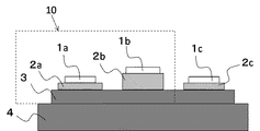
実施の形態1におけるパワーモジュールについて説明する。図1は、実施の形態1のパワーモジュールを示す平面図である。図2は、図1のA−A’線における断面図である。なお、図1、図2において、同一符号は同一又は相当部分を示し、以下も同様である。パワーモジュール100は、半導体素子1a、1b、1c(以下、1で代表する場合もある)がはんだを介して絶縁基板3の一方主面(上面)に接合されている回路パターン2a、2b,2c(以下、2で代表する場合もある)に接合し、絶縁基板3の主面に対向する絶縁基板3の他面(下面)に銅ベース4がはんだを介して接合される構成である。なお、銅ベース4はモジュール基板の一例である。
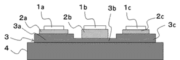
また、図2に示すような同一の絶縁基板上に回路パターンを介して一列に載置された半導体素子が3つの場合は、両端に位置する2つの半導体素子により1つの半導体素子が挟まれる。さらに、同一の絶縁基板上に回路パターンを介して載置された半導体素子が一列に並べられた5個である場合は、両端に位置する2つの半導体素子により3つの半導体素子が挟まれる。なお、実施例に限らず、半導体素子の個数は少なくとも3つ以上で一列に並んでいればよく、例えば、L字型に半導体素子を配置するパワーモジュールに対して、半導体素子を一列に配置することでパワーモジュールを小型化することができる。
実施の形態2のパワーモジュールについて説明する。図4は、実施の形態2のパワーモジュールを示す断面図である。実施の形態2のパワーモジュールは、実施の形態1のパワーモジュールにおいて、半導体素子が搭載される絶縁基板の厚みが同一であるのに対して、絶縁基板の厚みが同一でない点が異なる。
Claims (3)
- 一方主面に回路パターンが接合された絶縁基板と、
前記回路パターンと接合して前記絶縁基板に一列状に載置された少なくとも3つ以上のパワー半導体素子を有するパワーモジュールであって、
前記パワー半導体素子のうち、両端に位置する第1パワー半導体素子と第2パワー半導体素子とに挟まれて位置する第3パワー半導体素子の直下の前記回路パターンの前記主面に対する垂直方向の厚みは、前記第1パワー半導体素子又は前記第2パワー半導体素子の直下の前記回路パターンの前記主面に対する垂直方向の厚みより大きいことを特徴とするパワーモジュール。 - 前記第1パワー半導体素子又は前記第2パワー半導体素子の直下の前記回路パターンと前記主面との接合部から前記主面に対向する前記絶縁基板の他面までの前記主面に対する垂直方向の前記絶縁基板厚みは、前記第3パワー半導体素子の直下の前記回路パターンと前記主面との接合部から前記他面までの前記主面に対する垂直方向の前記絶縁基板の厚みより大きいことを特徴とする請求項1に記載のパワーモジュール。
- 前記第3パワー半導体素子の直下に位置する前記回路パターンは、銀で構成されていることを特徴とする請求項1又は2に記載のパワーモジュール。
Priority Applications (1)
| Application Number | Priority Date | Filing Date | Title |
|---|---|---|---|
| JP2016090263A JP6540587B2 (ja) | 2016-04-28 | 2016-04-28 | パワーモジュール |
Applications Claiming Priority (1)
| Application Number | Priority Date | Filing Date | Title |
|---|---|---|---|
| JP2016090263A JP6540587B2 (ja) | 2016-04-28 | 2016-04-28 | パワーモジュール |
Publications (2)
| Publication Number | Publication Date |
|---|---|
| JP2017199830A JP2017199830A (ja) | 2017-11-02 |
| JP6540587B2 true JP6540587B2 (ja) | 2019-07-10 |
Family
ID=60238234
Family Applications (1)
| Application Number | Title | Priority Date | Filing Date |
|---|---|---|---|
| JP2016090263A Active JP6540587B2 (ja) | 2016-04-28 | 2016-04-28 | パワーモジュール |
Country Status (1)
| Country | Link |
|---|---|
| JP (1) | JP6540587B2 (ja) |
Families Citing this family (4)
| Publication number | Priority date | Publication date | Assignee | Title |
|---|---|---|---|---|
| CN211908640U (zh) * | 2020-05-19 | 2020-11-10 | 阳光电源股份有限公司 | 一种功率变换装置 |
| CN115004359A (zh) * | 2020-08-28 | 2022-09-02 | 富士电机株式会社 | 半导体装置 |
| JP2023109210A (ja) * | 2022-01-27 | 2023-08-08 | 三菱電機株式会社 | 半導体装置 |
| US20260011629A1 (en) * | 2024-07-02 | 2026-01-08 | Semiconductor Components Industries, Llc | Substrate with stepped conductive layer surface |
Family Cites Families (3)
| Publication number | Priority date | Publication date | Assignee | Title |
|---|---|---|---|---|
| JPS61139047A (ja) * | 1984-12-11 | 1986-06-26 | Toshiba Corp | 半導体装置 |
| US7898807B2 (en) * | 2009-03-09 | 2011-03-01 | General Electric Company | Methods for making millichannel substrate, and cooling device and apparatus using the substrate |
| DE102009033029A1 (de) * | 2009-07-02 | 2011-01-05 | Electrovac Ag | Elektronische Vorrichtung |
-
2016
- 2016-04-28 JP JP2016090263A patent/JP6540587B2/ja active Active
Also Published As
| Publication number | Publication date |
|---|---|
| JP2017199830A (ja) | 2017-11-02 |
Similar Documents
| Publication | Publication Date | Title |
|---|---|---|
| CN111261598B (zh) | 封装结构及其适用的电源模块 | |
| JP6217756B2 (ja) | 半導体モジュール | |
| KR102586458B1 (ko) | 반도체 서브 어셈블리 및 반도체 파워 모듈 | |
| JP7060104B2 (ja) | 半導体装置 | |
| JP2021141220A (ja) | 半導体モジュール | |
| KR20130115456A (ko) | 반도체 패키지, 반도체 모듈, 및 그 실장 구조 | |
| JP2013197560A (ja) | パワー半導体モジュール | |
| JP2021180234A (ja) | 半導体モジュール | |
| WO2015005181A1 (ja) | 電力変換部品 | |
| WO2022059251A1 (ja) | 半導体装置 | |
| JP2016174034A (ja) | 半導体パワーモジュール | |
| JP2005116702A (ja) | パワー半導体モジュール | |
| JP2017199830A (ja) | パワーモジュール | |
| JP5477157B2 (ja) | 半導体装置 | |
| JP5429413B2 (ja) | 半導体装置 | |
| EP2178117A1 (en) | Power semiconductor module with double side cooling | |
| JP7306294B2 (ja) | 半導体モジュール | |
| JP5177174B2 (ja) | 半導体装置 | |
| JPWO2018029801A1 (ja) | 半導体装置 | |
| JP5682511B2 (ja) | 半導体モジュール | |
| JP7582147B2 (ja) | 半導体装置 | |
| JP6827402B2 (ja) | 半導体装置 | |
| KR101897304B1 (ko) | 파워 모듈 | |
| CN107210281B (zh) | 带有改进的键合连接结构的功率半导体模块 | |
| JP2016001644A (ja) | 半導体モジュール |
Legal Events
| Date | Code | Title | Description |
|---|---|---|---|
| A621 | Written request for application examination |
Free format text: JAPANESE INTERMEDIATE CODE: A621 Effective date: 20180515 |
|
| A977 | Report on retrieval |
Free format text: JAPANESE INTERMEDIATE CODE: A971007 Effective date: 20190115 |
|
| A131 | Notification of reasons for refusal |
Free format text: JAPANESE INTERMEDIATE CODE: A131 Effective date: 20190122 |
|
| A521 | Request for written amendment filed |
Free format text: JAPANESE INTERMEDIATE CODE: A523 Effective date: 20190215 |
|
| TRDD | Decision of grant or rejection written | ||
| A01 | Written decision to grant a patent or to grant a registration (utility model) |
Free format text: JAPANESE INTERMEDIATE CODE: A01 Effective date: 20190514 |
|
| A61 | First payment of annual fees (during grant procedure) |
Free format text: JAPANESE INTERMEDIATE CODE: A61 Effective date: 20190527 |
|
| R151 | Written notification of patent or utility model registration |
Ref document number: 6540587 Country of ref document: JP Free format text: JAPANESE INTERMEDIATE CODE: R151 |
|
| R250 | Receipt of annual fees |
Free format text: JAPANESE INTERMEDIATE CODE: R250 |
|
| R250 | Receipt of annual fees |
Free format text: JAPANESE INTERMEDIATE CODE: R250 |
|
| R250 | Receipt of annual fees |
Free format text: JAPANESE INTERMEDIATE CODE: R250 |
|
| R250 | Receipt of annual fees |
Free format text: JAPANESE INTERMEDIATE CODE: R250 |