JP6560444B2 - 半導体装置 - Google Patents
半導体装置 Download PDFInfo
- Publication number
- JP6560444B2 JP6560444B2 JP2018511559A JP2018511559A JP6560444B2 JP 6560444 B2 JP6560444 B2 JP 6560444B2 JP 2018511559 A JP2018511559 A JP 2018511559A JP 2018511559 A JP2018511559 A JP 2018511559A JP 6560444 B2 JP6560444 B2 JP 6560444B2
- Authority
- JP
- Japan
- Prior art keywords
- region
- well
- area
- semiconductor device
- well region
- Prior art date
- Legal status (The legal status is an assumption and is not a legal conclusion. Google has not performed a legal analysis and makes no representation as to the accuracy of the status listed.)
- Active
Links
Images


Classifications
-
- H—ELECTRICITY
- H10—SEMICONDUCTOR DEVICES; ELECTRIC SOLID-STATE DEVICES NOT OTHERWISE PROVIDED FOR
- H10D—INORGANIC ELECTRIC SEMICONDUCTOR DEVICES
- H10D62/00—Semiconductor bodies, or regions thereof, of devices having potential barriers
- H10D62/10—Shapes, relative sizes or dispositions of the regions of the semiconductor bodies; Shapes of the semiconductor bodies
- H10D62/102—Constructional design considerations for preventing surface leakage or controlling electric field concentration
- H10D62/103—Constructional design considerations for preventing surface leakage or controlling electric field concentration for increasing or controlling the breakdown voltage of reverse-biased devices
- H10D62/105—Constructional design considerations for preventing surface leakage or controlling electric field concentration for increasing or controlling the breakdown voltage of reverse-biased devices by having particular doping profiles, shapes or arrangements of PN junctions; by having supplementary regions, e.g. junction termination extension [JTE]
- H10D62/106—Constructional design considerations for preventing surface leakage or controlling electric field concentration for increasing or controlling the breakdown voltage of reverse-biased devices by having particular doping profiles, shapes or arrangements of PN junctions; by having supplementary regions, e.g. junction termination extension [JTE] having supplementary regions doped oppositely to or in rectifying contact with regions of the semiconductor bodies, e.g. guard rings with PN or Schottky junctions
-
- H—ELECTRICITY
- H10—SEMICONDUCTOR DEVICES; ELECTRIC SOLID-STATE DEVICES NOT OTHERWISE PROVIDED FOR
- H10D—INORGANIC ELECTRIC SEMICONDUCTOR DEVICES
- H10D12/00—Bipolar devices controlled by the field effect, e.g. insulated-gate bipolar transistors [IGBT]
- H10D12/01—Manufacture or treatment
- H10D12/031—Manufacture or treatment of IGBTs
-
- H—ELECTRICITY
- H10—SEMICONDUCTOR DEVICES; ELECTRIC SOLID-STATE DEVICES NOT OTHERWISE PROVIDED FOR
- H10D—INORGANIC ELECTRIC SEMICONDUCTOR DEVICES
- H10D30/00—Field-effect transistors [FET]
- H10D30/60—Insulated-gate field-effect transistors [IGFET]
-
- H—ELECTRICITY
- H10—SEMICONDUCTOR DEVICES; ELECTRIC SOLID-STATE DEVICES NOT OTHERWISE PROVIDED FOR
- H10D—INORGANIC ELECTRIC SEMICONDUCTOR DEVICES
- H10D30/00—Field-effect transistors [FET]
- H10D30/60—Insulated-gate field-effect transistors [IGFET]
- H10D30/63—Vertical IGFETs
- H10D30/635—Vertical IGFETs having no inversion channels, e.g. vertical accumulation channel FETs [ACCUFET] or normally-on vertical IGFETs
-
- H—ELECTRICITY
- H10—SEMICONDUCTOR DEVICES; ELECTRIC SOLID-STATE DEVICES NOT OTHERWISE PROVIDED FOR
- H10D—INORGANIC ELECTRIC SEMICONDUCTOR DEVICES
- H10D30/00—Field-effect transistors [FET]
- H10D30/60—Insulated-gate field-effect transistors [IGFET]
- H10D30/64—Double-diffused metal-oxide semiconductor [DMOS] FETs
- H10D30/66—Vertical DMOS [VDMOS] FETs
-
- H—ELECTRICITY
- H10—SEMICONDUCTOR DEVICES; ELECTRIC SOLID-STATE DEVICES NOT OTHERWISE PROVIDED FOR
- H10D—INORGANIC ELECTRIC SEMICONDUCTOR DEVICES
- H10D62/00—Semiconductor bodies, or regions thereof, of devices having potential barriers
- H10D62/10—Shapes, relative sizes or dispositions of the regions of the semiconductor bodies; Shapes of the semiconductor bodies
-
- H—ELECTRICITY
- H10—SEMICONDUCTOR DEVICES; ELECTRIC SOLID-STATE DEVICES NOT OTHERWISE PROVIDED FOR
- H10D—INORGANIC ELECTRIC SEMICONDUCTOR DEVICES
- H10D62/00—Semiconductor bodies, or regions thereof, of devices having potential barriers
- H10D62/10—Shapes, relative sizes or dispositions of the regions of the semiconductor bodies; Shapes of the semiconductor bodies
- H10D62/102—Constructional design considerations for preventing surface leakage or controlling electric field concentration
- H10D62/103—Constructional design considerations for preventing surface leakage or controlling electric field concentration for increasing or controlling the breakdown voltage of reverse-biased devices
- H10D62/105—Constructional design considerations for preventing surface leakage or controlling electric field concentration for increasing or controlling the breakdown voltage of reverse-biased devices by having particular doping profiles, shapes or arrangements of PN junctions; by having supplementary regions, e.g. junction termination extension [JTE]
-
- H—ELECTRICITY
- H10—SEMICONDUCTOR DEVICES; ELECTRIC SOLID-STATE DEVICES NOT OTHERWISE PROVIDED FOR
- H10D—INORGANIC ELECTRIC SEMICONDUCTOR DEVICES
- H10D62/00—Semiconductor bodies, or regions thereof, of devices having potential barriers
- H10D62/10—Shapes, relative sizes or dispositions of the regions of the semiconductor bodies; Shapes of the semiconductor bodies
- H10D62/102—Constructional design considerations for preventing surface leakage or controlling electric field concentration
- H10D62/103—Constructional design considerations for preventing surface leakage or controlling electric field concentration for increasing or controlling the breakdown voltage of reverse-biased devices
- H10D62/105—Constructional design considerations for preventing surface leakage or controlling electric field concentration for increasing or controlling the breakdown voltage of reverse-biased devices by having particular doping profiles, shapes or arrangements of PN junctions; by having supplementary regions, e.g. junction termination extension [JTE]
- H10D62/106—Constructional design considerations for preventing surface leakage or controlling electric field concentration for increasing or controlling the breakdown voltage of reverse-biased devices by having particular doping profiles, shapes or arrangements of PN junctions; by having supplementary regions, e.g. junction termination extension [JTE] having supplementary regions doped oppositely to or in rectifying contact with regions of the semiconductor bodies, e.g. guard rings with PN or Schottky junctions
- H10D62/107—Buried supplementary regions, e.g. buried guard rings
-
- H—ELECTRICITY
- H10—SEMICONDUCTOR DEVICES; ELECTRIC SOLID-STATE DEVICES NOT OTHERWISE PROVIDED FOR
- H10D—INORGANIC ELECTRIC SEMICONDUCTOR DEVICES
- H10D62/00—Semiconductor bodies, or regions thereof, of devices having potential barriers
- H10D62/10—Shapes, relative sizes or dispositions of the regions of the semiconductor bodies; Shapes of the semiconductor bodies
- H10D62/124—Shapes, relative sizes or dispositions of the regions of semiconductor bodies or of junctions between the regions
- H10D62/126—Top-view geometrical layouts of the regions or the junctions
- H10D62/127—Top-view geometrical layouts of the regions or the junctions of cellular field-effect devices, e.g. multicellular DMOS transistors or IGBTs
-
- H—ELECTRICITY
- H10—SEMICONDUCTOR DEVICES; ELECTRIC SOLID-STATE DEVICES NOT OTHERWISE PROVIDED FOR
- H10D—INORGANIC ELECTRIC SEMICONDUCTOR DEVICES
- H10D62/00—Semiconductor bodies, or regions thereof, of devices having potential barriers
- H10D62/10—Shapes, relative sizes or dispositions of the regions of the semiconductor bodies; Shapes of the semiconductor bodies
- H10D62/17—Semiconductor regions connected to electrodes not carrying current to be rectified, amplified or switched, e.g. channel regions
- H10D62/393—Body regions of DMOS transistors or IGBTs
-
- H—ELECTRICITY
- H10—SEMICONDUCTOR DEVICES; ELECTRIC SOLID-STATE DEVICES NOT OTHERWISE PROVIDED FOR
- H10D—INORGANIC ELECTRIC SEMICONDUCTOR DEVICES
- H10D62/00—Semiconductor bodies, or regions thereof, of devices having potential barriers
- H10D62/80—Semiconductor bodies, or regions thereof, of devices having potential barriers characterised by the materials
- H10D62/81—Semiconductor bodies, or regions thereof, of devices having potential barriers characterised by the materials of structures exhibiting quantum-confinement effects, e.g. single quantum wells; of structures having periodic or quasi-periodic potential variation
-
- H—ELECTRICITY
- H10—SEMICONDUCTOR DEVICES; ELECTRIC SOLID-STATE DEVICES NOT OTHERWISE PROVIDED FOR
- H10D—INORGANIC ELECTRIC SEMICONDUCTOR DEVICES
- H10D62/00—Semiconductor bodies, or regions thereof, of devices having potential barriers
- H10D62/80—Semiconductor bodies, or regions thereof, of devices having potential barriers characterised by the materials
- H10D62/83—Semiconductor bodies, or regions thereof, of devices having potential barriers characterised by the materials being Group IV materials, e.g. B-doped Si or undoped Ge
- H10D62/832—Semiconductor bodies, or regions thereof, of devices having potential barriers characterised by the materials being Group IV materials, e.g. B-doped Si or undoped Ge being Group IV materials comprising two or more elements, e.g. SiGe
- H10D62/8325—Silicon carbide
-
- H—ELECTRICITY
- H10—SEMICONDUCTOR DEVICES; ELECTRIC SOLID-STATE DEVICES NOT OTHERWISE PROVIDED FOR
- H10D—INORGANIC ELECTRIC SEMICONDUCTOR DEVICES
- H10D8/00—Diodes
- H10D8/60—Schottky-barrier diodes
-
- H—ELECTRICITY
- H10—SEMICONDUCTOR DEVICES; ELECTRIC SOLID-STATE DEVICES NOT OTHERWISE PROVIDED FOR
- H10D—INORGANIC ELECTRIC SEMICONDUCTOR DEVICES
- H10D84/00—Integrated devices formed in or on semiconductor substrates that comprise only semiconducting layers, e.g. on Si wafers or on GaAs-on-Si wafers
-
- H—ELECTRICITY
- H10—SEMICONDUCTOR DEVICES; ELECTRIC SOLID-STATE DEVICES NOT OTHERWISE PROVIDED FOR
- H10D—INORGANIC ELECTRIC SEMICONDUCTOR DEVICES
- H10D84/00—Integrated devices formed in or on semiconductor substrates that comprise only semiconducting layers, e.g. on Si wafers or on GaAs-on-Si wafers
- H10D84/101—Integrated devices comprising main components and built-in components, e.g. IGBT having built-in freewheel diode
- H10D84/141—VDMOS having built-in components
- H10D84/146—VDMOS having built-in components the built-in components being Schottky barrier diodes
-
- H—ELECTRICITY
- H10—SEMICONDUCTOR DEVICES; ELECTRIC SOLID-STATE DEVICES NOT OTHERWISE PROVIDED FOR
- H10D—INORGANIC ELECTRIC SEMICONDUCTOR DEVICES
- H10D84/00—Integrated devices formed in or on semiconductor substrates that comprise only semiconducting layers, e.g. on Si wafers or on GaAs-on-Si wafers
- H10D84/80—Integrated devices formed in or on semiconductor substrates that comprise only semiconducting layers, e.g. on Si wafers or on GaAs-on-Si wafers characterised by the integration of at least one component covered by groups H10D12/00 or H10D30/00, e.g. integration of IGFETs
- H10D84/86—Integrated devices formed in or on semiconductor substrates that comprise only semiconducting layers, e.g. on Si wafers or on GaAs-on-Si wafers characterised by the integration of at least one component covered by groups H10D12/00 or H10D30/00, e.g. integration of IGFETs of Schottky-barrier gate FETs
Landscapes
- Electrodes Of Semiconductors (AREA)
Description
以下、本実施の形態に関する半導体装置について説明する。説明の便宜上、まず、SBD内臓のMOSFETについて説明する。
本願明細書に記載される実施の形態においては、半導体装置の一例として、炭化珪素(SiC)半導体装置であり、第1の導電型をn型、第2の導電型をp型としたnチャネル炭化珪素MOSFETを例に挙げて説明する。途中、電位の高低について述べる場合があるが、第1の導電型をp型、第2の導電型をn型とした場合には、その電位の高低の記述も逆となる。
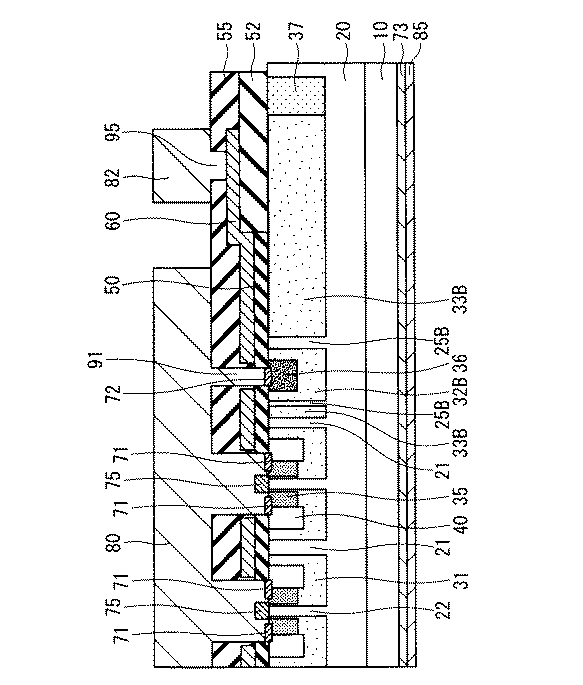
次に、本実施の形態に関するSBD内蔵MOSFETの動作を説明する。半導体材料として炭化珪素を例に考える。この場合、pn接合の拡散電位は略2Vである。
まず、還流動作を考える。還流動作では、ソース電圧に対しドレイン電圧が低くなり、数Vの電圧が発生する。
次に、ターンオフ動作を例にスイッチング状態を考える。前述の通り、ターンオフ中は、ドレイン電極85の電位が急激に増大する。そして、ウェル領域32およびウェル領域33内にホールが発生する。
続いて、本実施の形態に関する半導体装置であるSBD内蔵のMOSFETの製造方法について説明する。
本実施の形態に関する半導体装置について説明する。以下では、以上に記載された実施の形態で説明された構成と同様の構成については同じ符号を付して図示し、その詳細な説明については適宜省略するものとする。
図3は、本実施の形態に関する半導体装置を実現するための構成を概略的に例示する断面図である。
本実施の形態に関する半導体装置について説明する。以下では、以上に記載された実施の形態で説明された構成と同様の構成については同じ符号を付して図示し、その詳細な説明については適宜省略するものとする。
図4は、本実施の形態に関する半導体装置を実現するための構成を概略的に例示する断面図である。また、図5は、本実施の形態に関する半導体装置を実現するための構成を概略的に例示する平面図である。
本実施の形態に関する半導体装置について説明する。以下では、以上に記載された実施の形態で説明された構成と同様の構成については同じ符号を付して図示し、その詳細な説明については適宜省略するものとする。
図6は、本実施の形態に関する半導体装置を実現するための構成を概略的に例示する断面図である。
本実施の形態に関する半導体装置について説明する。以下では、以上に記載された実施の形態で説明された構成と同様の構成については同じ符号を付して図示し、その詳細な説明については適宜省略するものとする。
図7は、本実施の形態に関する半導体装置を実現するための構成を概略的に例示する断面図である。
本実施の形態に関する半導体装置について説明する。以下では、以上に記載された実施の形態で説明された構成と同様の構成については同じ符号を付して図示し、その詳細な説明については適宜省略するものとする。
図8は、本実施の形態に関する半導体装置を実現するための構成を概略的に例示する断面図である。
本実施の形態に関する半導体装置について説明する。以下では、以上に記載された実施の形態で説明された構成と同様の構成については同じ符号を付して図示し、その詳細な説明については適宜省略するものとする。
図9は、本実施の形態に関する半導体装置を実現するための構成を概略的に例示する平面図である。
以下に、以上に記載された実施の形態によって生じる効果を例示する。なお、以下では、以上に記載された実施の形態に例示された具体的な構成に基づいて当該効果が記載されるが、同様の効果が生じる範囲で、本願明細書に例示される他の具体的な構成と置き換えられてもよい。
以上に記載された実施の形態では、ユニポーラ型ダイオードを内蔵したユニポーラ型トランジスタとして、SBD内蔵のMOSFETが例示された。しかしながら、上記の内容は、他のユニポーラ型デバイスにも応用することができる。
Claims (12)
- 第1の導電型の半導体基板の上面に設けられるワイドギャップ半導体層である、第1の導電型のドリフト層と、
前記ドリフト層の表層において互いに離間して複数設けられる、第2の導電型の第1のウェル領域と、
それぞれの前記第1のウェル領域の表層から深さ方向に貫通して設けられる、第1の導電型の第1の離間領域と、
それぞれの前記第1のウェル領域の表層に設けられる、第1の導電型のソース領域と、
前記第1の離間領域の上面に設けられる第1のショットキー電極と、
前記ソース領域の表層に少なくとも一部が設けられる第1のオーミック電極と、
前記ドリフト層の表層において複数の前記第1のウェル領域全体を平面視で挟んで設けられ、かつ、それぞれの前記第1のウェル領域よりも面積が広い、第2の導電型の第2のウェル領域と、
前記ドリフト層の表層において前記第2のウェル領域を平面視で挟んで設けられ、かつ、前記第2のウェル領域よりも面積が広い、第2の導電型の第3のウェル領域と、
前記第2のウェル領域の一部に設けられる第2のオーミック電極と、
前記第2のウェル領域と、前記第3のウェル領域との間に設けられる、第1の導電型の分断領域と、
前記第1のショットキー電極と、前記第1のオーミック電極と、前記第2のオーミック電極とに接続されるソース電極とを備え、
前記第3のウェル領域は、前記ソース電極へのオーミック接続を有さない、
半導体装置。 - 前記第2のウェル領域と前記第3のウェル領域との間に前記分断領域を介してパンチスルー電流が流れる、
請求項1に記載の半導体装置。 - 前記分断領域の上面は、絶縁体に接触する、
請求項1または請求項2に記載の半導体装置。 - 前記半導体装置は、さらに、
前記ソース領域と前記ドリフト層とに挟まれる前記第1のウェル領域の上面にゲート絶縁膜を挟んで設けられるゲート電極を備え、
前記ゲート電極は、前記第3のウェル領域の上面に対応する領域にも設けられる、
請求項1から請求項3のうちのいずれか1項に記載の半導体装置。 - 前記分断領域の前記第2のウェル領域と前記第3のウェル領域とを結ぶ方向における幅をW、前記分断領域の実効不純物濃度をN、半導体の誘電率をε、素電荷をqとする場合、
請求項1から請求項4のうちのいずれか1項に記載の半導体装置。 - 前記分断領域は、平面視において、前記第2のオーミック電極を囲む、
請求項1から請求項5のうちのいずれか1項に記載の半導体装置。 - 前記半導体装置は、さらに、
前記第2のウェル領域の表層から深さ方向に貫通して設けられる、第1の導電型の第2の離間領域と、
前記第2の離間領域の上面に設けられる第2のショットキー電極とを備える、
請求項1から請求項6のうちのいずれか1項に記載の半導体装置。 - 前記半導体装置は、さらに、
前記第3のウェル領域の上面の少なくとも一部に設けられるフィールド絶縁膜を備え、
前記フィールド絶縁膜の厚さは、前記ゲート絶縁膜の厚さよりも厚く、
前記ゲート電極は、前記フィールド絶縁膜が設けられる領域においては、前記フィールド絶縁膜を挟んで前記第3のウェル領域の上面に設けられる、
請求項4に記載の半導体装置。 - 前記ゲート電極は、前記第3のウェル領域の上面に対応する領域においては、前記フィールド絶縁膜を挟んで前記第3のウェル領域の上面に設けられる、
請求項8に記載の半導体装置。 - 前記半導体装置は、さらに、
前記第3のウェル領域の表層に設けられる、第2の導電型のウェル注入領域を備え、
前記ウェル注入領域の不純物濃度は、前記第1のウェル領域の不純物濃度よりも高い、
請求項1から請求項9のうちのいずれか1項に記載の半導体装置。 - 前記半導体装置は、さらに、
前記分断領域の表層に設けられる、少なくとも1つの第2の導電型の補助導電領域を備え、
前記補助導電領域は、前記第2のウェル領域と第3のウェル領域とを電気的に接続する、
請求項1から請求項10のうちのいずれか1項に記載の半導体装置。 - 前記補助導電領域が設けられる長さの合計は、前記分断領域が設けられる長さの合計の1/10以下であり、
前記補助導電領域が設けられる長さは、前記補助導電領域が、前記第2のウェル領域と前記第3のウェル領域とを結ぶ方向と交差する方向において設けられる長さであり、
前記分断領域が設けられる長さは、前記分断領域が、前記第2のウェル領域と前記第3のウェル領域とを結ぶ方向と交差する方向において設けられる長さである、
請求項11に記載の半導体装置。
Applications Claiming Priority (1)
| Application Number | Priority Date | Filing Date | Title |
|---|---|---|---|
| PCT/JP2016/061706 WO2017179102A1 (ja) | 2016-04-11 | 2016-04-11 | 半導体装置 |
Related Child Applications (1)
| Application Number | Title | Priority Date | Filing Date |
|---|---|---|---|
| JP2019132446A Division JP6752336B2 (ja) | 2019-07-18 | 2019-07-18 | 半導体装置 |
Publications (2)
| Publication Number | Publication Date |
|---|---|
| JPWO2017179102A1 JPWO2017179102A1 (ja) | 2018-08-30 |
| JP6560444B2 true JP6560444B2 (ja) | 2019-08-14 |
Family
ID=60042498
Family Applications (1)
| Application Number | Title | Priority Date | Filing Date |
|---|---|---|---|
| JP2018511559A Active JP6560444B2 (ja) | 2016-04-11 | 2016-04-11 | 半導体装置 |
Country Status (5)
| Country | Link |
|---|---|
| US (1) | US11222973B2 (ja) |
| JP (1) | JP6560444B2 (ja) |
| CN (1) | CN108886038B (ja) |
| DE (1) | DE112016006723B4 (ja) |
| WO (1) | WO2017179102A1 (ja) |
Families Citing this family (11)
| Publication number | Priority date | Publication date | Assignee | Title |
|---|---|---|---|---|
| WO2017183375A1 (ja) | 2016-04-21 | 2017-10-26 | 三菱電機株式会社 | 半導体装置 |
| JP6641488B2 (ja) * | 2016-08-25 | 2020-02-05 | 三菱電機株式会社 | 半導体装置 |
| CN115274855B (zh) * | 2017-02-24 | 2025-10-28 | 三菱电机株式会社 | 碳化硅半导体装置以及电力变换装置 |
| JP6874158B2 (ja) * | 2017-12-19 | 2021-05-19 | 三菱電機株式会社 | 炭化珪素半導体装置および電力変換装置 |
| WO2019123717A1 (ja) * | 2017-12-19 | 2019-06-27 | 三菱電機株式会社 | 炭化珪素半導体装置および電力変換装置 |
| DE112018006467B4 (de) | 2017-12-19 | 2022-11-17 | Mitsubishi Electric Corporation | Siliciumcarbid-halbleiteranordnung und leistungswandler |
| CN114342089B (zh) * | 2019-09-06 | 2025-02-14 | 三菱电机株式会社 | 碳化硅半导体装置以及电力变换装置 |
| WO2021245992A1 (ja) * | 2020-06-04 | 2021-12-09 | 三菱電機株式会社 | 半導体装置および電力変換装置 |
| US20240250165A1 (en) * | 2021-07-07 | 2024-07-25 | Mitsubishi Electric Corporation | Silicon carbide semiconductor device and power converter using silicon carbide semiconductor device |
| US12315776B2 (en) * | 2021-11-08 | 2025-05-27 | Analog Devices, Inc. | Integrated device package with an integrated heat sink |
| JPWO2025127073A1 (ja) * | 2023-12-13 | 2025-06-19 |
Family Cites Families (19)
| Publication number | Priority date | Publication date | Assignee | Title |
|---|---|---|---|---|
| JP2858404B2 (ja) * | 1990-06-08 | 1999-02-17 | 株式会社デンソー | 絶縁ゲート型バイポーラトランジスタおよびその製造方法 |
| JP3850580B2 (ja) * | 1999-03-30 | 2006-11-29 | 株式会社東芝 | 半導体装置 |
| JP4538870B2 (ja) * | 1999-09-21 | 2010-09-08 | 株式会社デンソー | 炭化珪素半導体装置及びその製造方法 |
| JP5011612B2 (ja) * | 2000-10-31 | 2012-08-29 | 富士電機株式会社 | 半導体装置 |
| JP2003017701A (ja) | 2001-07-04 | 2003-01-17 | Denso Corp | 半導体装置 |
| JP4338178B2 (ja) | 2003-03-24 | 2009-10-07 | 財団法人電力中央研究所 | 炭化珪素半導体装置の検査方法および検査装置、並びに炭化珪素半導体装置の製造方法 |
| JP4585772B2 (ja) * | 2004-02-06 | 2010-11-24 | 関西電力株式会社 | 高耐圧ワイドギャップ半導体装置及び電力装置 |
| CN102265404B (zh) * | 2008-12-25 | 2014-06-11 | 三菱电机株式会社 | 功率用半导体装置 |
| JP4962664B2 (ja) * | 2009-10-14 | 2012-06-27 | 三菱電機株式会社 | 電力用半導体装置とその製造方法、ならびにパワーモジュール |
| WO2011161721A1 (ja) * | 2010-06-24 | 2011-12-29 | 三菱電機株式会社 | 電力用半導体装置 |
| WO2012001837A1 (ja) * | 2010-06-30 | 2012-01-05 | 三菱電機株式会社 | 電力用半導体装置 |
| CN103141026B (zh) | 2011-10-03 | 2014-04-02 | 松下电器产业株式会社 | 半导体装置、电力转换器及电力转换器的控制方法 |
| JP6072432B2 (ja) * | 2012-05-15 | 2017-02-01 | 三菱電機株式会社 | 半導体装置及びその製造方法 |
| WO2014038110A1 (ja) | 2012-09-06 | 2014-03-13 | 三菱電機株式会社 | 半導体装置 |
| JP5992094B2 (ja) | 2013-04-03 | 2016-09-14 | 三菱電機株式会社 | 半導体装置 |
| WO2014178262A1 (ja) * | 2013-04-30 | 2014-11-06 | 日産自動車株式会社 | 半導体装置及びその製造方法 |
| JP6244762B2 (ja) * | 2013-09-12 | 2017-12-13 | 住友電気工業株式会社 | 炭化珪素半導体装置 |
| DE102015207214A1 (de) * | 2014-05-21 | 2015-12-17 | Sumitomo Electric Industries, Ltd. | Siliziumkarbid-Halbleitervorrichtung |
| JP6058228B1 (ja) * | 2015-04-22 | 2017-01-11 | 三菱電機株式会社 | 半導体装置および半導体装置の製造方法 |
-
2016
- 2016-04-11 DE DE112016006723.2T patent/DE112016006723B4/de active Active
- 2016-04-11 US US16/082,212 patent/US11222973B2/en active Active
- 2016-04-11 JP JP2018511559A patent/JP6560444B2/ja active Active
- 2016-04-11 WO PCT/JP2016/061706 patent/WO2017179102A1/ja not_active Ceased
- 2016-04-11 CN CN201680084166.3A patent/CN108886038B/zh active Active
Also Published As
| Publication number | Publication date |
|---|---|
| JPWO2017179102A1 (ja) | 2018-08-30 |
| CN108886038B (zh) | 2023-05-02 |
| US11222973B2 (en) | 2022-01-11 |
| DE112016006723B4 (de) | 2024-12-12 |
| DE112016006723T5 (de) | 2018-12-20 |
| CN108886038A (zh) | 2018-11-23 |
| US20190181259A1 (en) | 2019-06-13 |
| WO2017179102A1 (ja) | 2017-10-19 |
Similar Documents
| Publication | Publication Date | Title |
|---|---|---|
| JP6560444B2 (ja) | 半導体装置 | |
| JP7786512B2 (ja) | 半導体装置 | |
| JP6641488B2 (ja) | 半導体装置 | |
| US20230017518A1 (en) | Semiconductor device | |
| JP6649183B2 (ja) | 半導体装置 | |
| US7700971B2 (en) | Insulated gate silicon carbide semiconductor device | |
| US7781786B2 (en) | Semiconductor device having a heterojunction diode and manufacturing method thereof | |
| JP5940235B1 (ja) | 半導体装置 | |
| US8933466B2 (en) | Semiconductor element | |
| JP7643621B2 (ja) | 半導体装置 | |
| JP2019054064A (ja) | 半導体装置 | |
| US9029874B2 (en) | Semiconductor device having a first silicon carbide semiconductor layer and a second silicon carbide semiconductor layer | |
| JP2016006854A (ja) | 半導体素子およびその製造方法 | |
| US20220336590A1 (en) | Silicon carbide semiconductor device and method for manufacturing the same | |
| JP2017069551A (ja) | 半導体素子 | |
| JP7196265B2 (ja) | 半導体装置 | |
| CN112466922A (zh) | 半导体装置 | |
| US12550397B2 (en) | Silicon carbide vertical conduction MOSFET device and manufacturing process thereof | |
| US20250203977A1 (en) | Silicon carbide vertical conduction mosfet device for power applications and manufacturing process thereof | |
| JP6752336B2 (ja) | 半導体装置 | |
| JP2008112774A (ja) | ワイドバンドギャップ半導体を用いた絶縁ゲート型半導体装置およびその製造方法 | |
| JP7628874B2 (ja) | 半導体装置及びその製造方法 | |
| JP4876418B2 (ja) | 半導体装置 | |
| CN118693125A (zh) | 半导体装置 |
Legal Events
| Date | Code | Title | Description |
|---|---|---|---|
| A521 | Request for written amendment filed | ||
| A621 | Written request for application examination | ||
| TRDD | Decision of grant or rejection written | ||
| A01 | Written decision to grant a patent or to grant a registration (utility model) |
Free format text: JAPANESE INTERMEDIATE CODE: A01 Effective date: 20190618 |
|
| A61 | First payment of annual fees (during grant procedure) |
Free format text: JAPANESE INTERMEDIATE CODE: A61 Effective date: 20190718 |
|
| R150 | Certificate of patent or registration of utility model |
Ref document number: 6560444 Country of ref document: JP Free format text: JAPANESE INTERMEDIATE CODE: R150 |
|
| R250 | Receipt of annual fees |
Free format text: JAPANESE INTERMEDIATE CODE: R250 |
|
| R250 | Receipt of annual fees |
Free format text: JAPANESE INTERMEDIATE CODE: R250 |
|
| R250 | Receipt of annual fees |
Free format text: JAPANESE INTERMEDIATE CODE: R250 |
|
| R250 | Receipt of annual fees |
Free format text: JAPANESE INTERMEDIATE CODE: R250 |