JP6561445B2 - 光増幅装置、光伝送装置、及び、光伝送システム - Google Patents
光増幅装置、光伝送装置、及び、光伝送システム Download PDFInfo
- Publication number
- JP6561445B2 JP6561445B2 JP2014202176A JP2014202176A JP6561445B2 JP 6561445 B2 JP6561445 B2 JP 6561445B2 JP 2014202176 A JP2014202176 A JP 2014202176A JP 2014202176 A JP2014202176 A JP 2014202176A JP 6561445 B2 JP6561445 B2 JP 6561445B2
- Authority
- JP
- Japan
- Prior art keywords
- optical
- wavelengths
- light
- wavelength
- node
- Prior art date
- Legal status (The legal status is an assumption and is not a legal conclusion. Google has not performed a legal analysis and makes no representation as to the accuracy of the status listed.)
- Active
Links
Images


Classifications
-
- H—ELECTRICITY
- H04—ELECTRIC COMMUNICATION TECHNIQUE
- H04B—TRANSMISSION
- H04B10/00—Transmission systems employing electromagnetic waves other than radio-waves, e.g. infrared, visible or ultraviolet light, or employing corpuscular radiation, e.g. quantum communication
- H04B10/29—Repeaters
- H04B10/291—Repeaters in which processing or amplification is carried out without conversion of the main signal from optical form
- H04B10/293—Signal power control
- H04B10/294—Signal power control in a multiwavelength system, e.g. gain equalisation
- H04B10/296—Transient power control, e.g. due to channel add/drop or rapid fluctuations in the input power
-
- G—PHYSICS
- G02—OPTICS
- G02B—OPTICAL ELEMENTS, SYSTEMS OR APPARATUS
- G02B6/00—Light guides; Structural details of arrangements comprising light guides and other optical elements, e.g. couplings
- G02B6/24—Coupling light guides
- G02B6/26—Optical coupling means
- G02B6/28—Optical coupling means having data bus means, i.e. plural waveguides interconnected and providing an inherently bidirectional system by mixing and splitting signals
- G02B6/293—Optical coupling means having data bus means, i.e. plural waveguides interconnected and providing an inherently bidirectional system by mixing and splitting signals with wavelength selective means
- G02B6/29379—Optical coupling means having data bus means, i.e. plural waveguides interconnected and providing an inherently bidirectional system by mixing and splitting signals with wavelength selective means characterised by the function or use of the complete device
- G02B6/2938—Optical coupling means having data bus means, i.e. plural waveguides interconnected and providing an inherently bidirectional system by mixing and splitting signals with wavelength selective means characterised by the function or use of the complete device for multiplexing or demultiplexing, i.e. combining or separating wavelengths, e.g. 1xN, NxM
-
- H—ELECTRICITY
- H01—ELECTRIC ELEMENTS
- H01S—DEVICES USING THE PROCESS OF LIGHT AMPLIFICATION BY STIMULATED EMISSION OF RADIATION [LASER] TO AMPLIFY OR GENERATE LIGHT; DEVICES USING STIMULATED EMISSION OF ELECTROMAGNETIC RADIATION IN WAVE RANGES OTHER THAN OPTICAL
- H01S3/00—Lasers, i.e. devices using stimulated emission of electromagnetic radiation in the infrared, visible or ultraviolet wave range
- H01S3/05—Construction or shape of optical resonators; Accommodation of active medium therein; Shape of active medium
- H01S3/06—Construction or shape of active medium
- H01S3/063—Waveguide lasers, i.e. whereby the dimensions of the waveguide are of the order of the light wavelength
- H01S3/067—Fibre lasers
- H01S3/06754—Fibre amplifiers
- H01S3/06758—Tandem amplifiers
-
- H—ELECTRICITY
- H01—ELECTRIC ELEMENTS
- H01S—DEVICES USING THE PROCESS OF LIGHT AMPLIFICATION BY STIMULATED EMISSION OF RADIATION [LASER] TO AMPLIFY OR GENERATE LIGHT; DEVICES USING STIMULATED EMISSION OF ELECTROMAGNETIC RADIATION IN WAVE RANGES OTHER THAN OPTICAL
- H01S3/00—Lasers, i.e. devices using stimulated emission of electromagnetic radiation in the infrared, visible or ultraviolet wave range
- H01S3/10—Controlling the intensity, frequency, phase, polarisation or direction of the emitted radiation, e.g. switching, gating, modulating or demodulating
- H01S3/13—Stabilisation of laser output parameters, e.g. frequency or amplitude
- H01S3/1301—Stabilisation of laser output parameters, e.g. frequency or amplitude in optical amplifiers
- H01S3/13013—Stabilisation of laser output parameters, e.g. frequency or amplitude in optical amplifiers by controlling the optical pumping
-
- H—ELECTRICITY
- H01—ELECTRIC ELEMENTS
- H01S—DEVICES USING THE PROCESS OF LIGHT AMPLIFICATION BY STIMULATED EMISSION OF RADIATION [LASER] TO AMPLIFY OR GENERATE LIGHT; DEVICES USING STIMULATED EMISSION OF ELECTROMAGNETIC RADIATION IN WAVE RANGES OTHER THAN OPTICAL
- H01S3/00—Lasers, i.e. devices using stimulated emission of electromagnetic radiation in the infrared, visible or ultraviolet wave range
- H01S3/10—Controlling the intensity, frequency, phase, polarisation or direction of the emitted radiation, e.g. switching, gating, modulating or demodulating
- H01S3/13—Stabilisation of laser output parameters, e.g. frequency or amplitude
- H01S3/1305—Feedback control systems
Landscapes
- Physics & Mathematics (AREA)
- Electromagnetism (AREA)
- Engineering & Computer Science (AREA)
- Optics & Photonics (AREA)
- Plasma & Fusion (AREA)
- Computer Networks & Wireless Communication (AREA)
- Signal Processing (AREA)
- General Physics & Mathematics (AREA)
- Optical Communication System (AREA)
- Lasers (AREA)
Description
図2は、上述したノード2の第1構成例を示すブロック図である。図2に示すノード2は、例示的に、光挿入分岐装置(OADM:Optical Add-Drop Multiplexer)であり、光増幅部21、励起光源22、分岐部(ドロップ部)23、合波部(アド部)24、光増幅部25、励起光源26、及び、制御部27を備える。なお、「光増幅部」を備えたノード2は、「光増幅装置」に相当すると捉えてもよい(以下、同様。)。
なお、図2において、励起光パワーの制御対象は、励起LD22及び26の双方又は一方でもよい。ノード2において、光伝送路3へ送信されるWDM光の1波長あたりの送信光パワーが増加できれば、送信光パワーの制御手法や制御対象は特に問わない(以下、同様。)。
なお、図2に例示したノード2は、受信アンプ21及び送信アンプ25の双方を備えるが、いずれか一方が備えられない構成であってもよい。別言すると、上述した設定波長数情報に応じた励起光パワーの設定、制御は、受信アンプ21及び送信アンプ25の一方しか備えられないノード2にも適用可能である。
図2の第1構成例において、設定波長数情報は、例えば図5に示すように、光増幅部21及び25の一方又は双方に与えられてもよい。光増幅部21及び25は、それぞれ、設定波長数情報を基に、励起LD22及び26の励起光パワーを設定波長数に応じたパワーに設定、制御することが可能である。
図2に例示した合波部24には、波長のクロスコネクト(XC)情報が設定されることがある。クロスコネクト情報には、WDM光に含まれ得る波長のうち、どの波長のアド光をWDM光にアドするかを識別可能な情報が含まれてよい。
図2に例示した合波部24の後段には、例えば図7に示すように、光チャネルモニタ(OCM)28が備えられることがある。OCM28は、WDM光に含まれる波長毎に光パワーレベル等をモニタすることが可能である。なお、OCM28は、合波部24に内蔵されていてもよい。
図7に例示したOCM28は、例えば図8に示すように、光増幅部25の後段(あるいは内部でもよい。)に備えられることもある。ただし、OCM28は、合波部24の後段(あるいは内部)と、光増幅部25の後段(あるいは内部)と、のそれぞれに備えられても構わない。
図6〜図8に示した構成例では、クロスコネクト情報やモニタ情報から取得あるいは識別した波長数(以下、便宜的に「運用波長数」と称することがある。)が、所期の設定波長数以下になっているか否かを監視することができる。「所期の設定波長数」は、例示的に、運用可能な最大波長数としてノード2に設定(制限)された波長数を意味する。
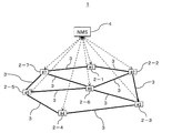
図10は、図1に例示したノード2−1〜2−5をそれぞれ経由する光経路に着目した光伝送システム1の構成例を示すブロック図である。ノード2−1〜2−5は、それぞれ、OADMノード、ILAノード、及び、HUBノードのいずれであっても構わない。
NMS4によって各ノード2が集中的に監視されている光ネットワーク1では、NMS4において、相対的に他のスパンよりも伝送路損失が大きい(例えば、最大の)スパンを識別可能である。スパンのOSNRの劣化量は、当該スパンの伝送路損失が支配的であると捉えてよい。
図15は、図13に例示した光ネットワーク1の変形例を示すブロック図である。図15に示す光ネットワーク1は、図13の構成例に比して、例示的に、ノード2−1とノード2−4との間に、ノード2−2−1、ノード2−2−2、ノード2−3−1、及び、ノード2−3−2を備える点が異なる。
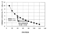
既述の波長数制限スパンでは、WDM光における波長間隔(「波長グリッド」と称してもよい。)を、波長数制限前の波長間隔よりも広げることが可能である。
図17に、図16により上述した波長間隔制御の一例を示す。なお、図17に例示するフローチャートの処理は、例示的に、波長数制限スパン#2の送信ノード#2において実施されてよい。
2−1〜2−n(#1〜#n) 光伝送装置(ノード)
2−2−1,2−2−2,2−3−1,2−3−2 光伝送装置(ノード)
3 光伝送路
4 NMS
5 光受信器
6 光送信器
21 光増幅部(受信アンプ、プリアンプ)
21a 光増幅部
22,22a,26 励起光源
23 分岐(ドロップ)部
24 合波(アド)部
25 光増幅部(送信アンプ、ポストアンプ)
27,27a,27b,27c,27d 制御部
28 モニタ(OCM)
Claims (12)
- 複数の波長の光を含む波長多重光が入力され、前記波長多重光を増幅する光増幅装置において、
励起光を出力する励起光部と、
前記励起光のパワーレベルに応じて、前記波長多重光を増幅する光増幅部と、を有し、
前記光増幅装置に入力される波長多重光の波長数は、前記光増幅装置に入力される可能性のある最大の波長数として設定された最大波長数以下の波長数であり、
前記励起光のパワーレベルを前記最大波長数に基づいて決定することで前記波長多重光の一波長あたりの増幅利得を増加させることを特徴とする光増幅装置。 - 前記励起光のパワーレベルを制御する制御部を備え、
前記制御部は、設定された前記最大波長数に基づいて、前記励起光のパワーレベルを制御する、請求項1に記載の光増幅装置。 - 前記最大波長数の設定は、前記光増幅装置を含む光ネットワークのマネージメントを行なうネットワークマネージメントシステムから前記制御部に対して行なわれる、請求項2に記載の光増幅装置。
- 前記最大波長数の設定は、前記光増幅装置に対して設定された、波長数の装置設定情報に基づいて行なわれる、請求項2に記載の光増幅装置。
- 前記励起光のパワーレベルを制御する制御部と、
前記波長多重光の波長数をモニタするモニタと、を備え、
前記制御部は、前記モニタによってモニタされた波長数を基に、前記最大波長数の設定を行なう、請求項1に記載の光増幅装置。 - 前記制御部は、
前記モニタによってモニタされた波長数が前記設定した最大波長数を超えると、アラームを出力する、請求項5に記載の光増幅装置。 - 前記制御部は、
前記設定された最大波長数以下の波長数に応じて、前記波長多重光の波長間隔を拡大制御する、請求項2に記載の光増幅装置。 - 複数の波長の光を含む波長多重光が入力され、前記波長多重光を増幅する光増幅装置において、
励起光を出力する励起光部と、
前記励起光のパワーレベルに応じて、前記波長多重光を増幅する光増幅部と、を有し、
前記光増幅装置に入力される波長多重光の波長数は、前記光増幅装置に入力される可能性のある最大の波長数として設定された最大波長数以下の波長数であり、
前記光増幅部の出力光パワーレベルの設定値は、前記最大波長数に基づいて決定されることを特徴とする光増幅装置。 - 前記励起光のパワーレベルは、前記光増幅部の出力光パワーレベルの設定値に基づいて決定される、請求項8に記載の光増幅装置。
- 請求項1〜9のいずれか1項に記載の光増幅装置を備えた光伝送装置。
- 複数の光伝送装置を備えた光伝送システムであって、
前記光伝送装置のいずれかが、請求項1〜9のいずれか1項に記載の光増幅装置を備えた光伝送装置である、光伝送システム。 - 前記光増幅装置を備えた光伝送装置は、光伝送損失が他の伝送区間よりも大きい伝送区間の送信側に配置された、請求項11に記載の光伝送システム。
Priority Applications (2)
| Application Number | Priority Date | Filing Date | Title |
|---|---|---|---|
| JP2014202176A JP6561445B2 (ja) | 2014-09-30 | 2014-09-30 | 光増幅装置、光伝送装置、及び、光伝送システム |
| US14/829,939 US9391421B2 (en) | 2014-09-30 | 2015-08-19 | Optical amplification apparatus, optical transmission apparatus, and optical transmission system |
Applications Claiming Priority (1)
| Application Number | Priority Date | Filing Date | Title |
|---|---|---|---|
| JP2014202176A JP6561445B2 (ja) | 2014-09-30 | 2014-09-30 | 光増幅装置、光伝送装置、及び、光伝送システム |
Publications (2)
| Publication Number | Publication Date |
|---|---|
| JP2016072886A JP2016072886A (ja) | 2016-05-09 |
| JP6561445B2 true JP6561445B2 (ja) | 2019-08-21 |
Family
ID=55585469
Family Applications (1)
| Application Number | Title | Priority Date | Filing Date |
|---|---|---|---|
| JP2014202176A Active JP6561445B2 (ja) | 2014-09-30 | 2014-09-30 | 光増幅装置、光伝送装置、及び、光伝送システム |
Country Status (2)
| Country | Link |
|---|---|
| US (1) | US9391421B2 (ja) |
| JP (1) | JP6561445B2 (ja) |
Cited By (1)
| Publication number | Priority date | Publication date | Assignee | Title |
|---|---|---|---|---|
| JP2025506067A (ja) * | 2022-02-22 | 2025-03-05 | 華為技術有限公司 | 光学コンポーネント、光スイッチング完全相互接続システム、および通信システム |
Families Citing this family (5)
| Publication number | Priority date | Publication date | Assignee | Title |
|---|---|---|---|---|
| JP6365256B2 (ja) * | 2014-11-18 | 2018-08-01 | 富士通株式会社 | 光伝送システム、光受信装置、管理装置及び信号調整方法 |
| JP6485189B2 (ja) * | 2015-04-23 | 2019-03-20 | 富士通株式会社 | 光伝送システムおよび光伝送装置 |
| US11177885B2 (en) * | 2017-04-10 | 2021-11-16 | Nec Corporation | Repeater and repeating method |
| US20200252700A1 (en) | 2017-10-27 | 2020-08-06 | Nec Corporation | Resource allocation device and resource allocation method |
| JP7714841B2 (ja) * | 2021-11-17 | 2025-07-30 | Ntt株式会社 | 光伝送システム、光伝送方法及びプログラム |
Family Cites Families (10)
| Publication number | Priority date | Publication date | Assignee | Title |
|---|---|---|---|---|
| JPH0964819A (ja) * | 1995-08-23 | 1997-03-07 | Fujitsu Ltd | 光システム |
| JPH10229386A (ja) * | 1997-02-17 | 1998-08-25 | Nec Corp | 光ファイバアンプとこれを用いた光通信システム |
| JP3068500B2 (ja) * | 1997-04-25 | 2000-07-24 | 日本電気株式会社 | 光信号増幅伝送方式 |
| JP3338007B2 (ja) * | 1999-09-10 | 2002-10-28 | 古河電気工業株式会社 | 光増幅器及び波長多重光通信システム |
| JP2002353939A (ja) * | 2001-05-25 | 2002-12-06 | Kddi Submarine Cable Systems Inc | 光送信装置 |
| US6989923B2 (en) * | 2001-08-08 | 2006-01-24 | Photuris, Inc. | Optical amplifier having automatic gain control with improved performance |
| JP3933514B2 (ja) * | 2002-04-23 | 2007-06-20 | 古河電気工業株式会社 | 光増幅器およびその光増幅器を用いた光通信システム |
| JP5135849B2 (ja) * | 2007-03-30 | 2013-02-06 | 富士通株式会社 | 利得制御装置,光伝送装置および光増幅器の利得制御方法 |
| JP5079669B2 (ja) * | 2008-11-20 | 2012-11-21 | 日本電信電話株式会社 | 光ネットワークシステム |
| WO2010107061A1 (ja) * | 2009-03-18 | 2010-09-23 | 日本電気株式会社 | 光伝送装置、運用波長数制限方法及びプログラム |
-
2014
- 2014-09-30 JP JP2014202176A patent/JP6561445B2/ja active Active
-
2015
- 2015-08-19 US US14/829,939 patent/US9391421B2/en active Active
Cited By (2)
| Publication number | Priority date | Publication date | Assignee | Title |
|---|---|---|---|---|
| JP2025506067A (ja) * | 2022-02-22 | 2025-03-05 | 華為技術有限公司 | 光学コンポーネント、光スイッチング完全相互接続システム、および通信システム |
| JP7839289B2 (ja) | 2022-02-22 | 2026-04-01 | 華為技術有限公司 | 光学コンポーネント、光スイッチング完全相互接続システム、および通信システム |
Also Published As
| Publication number | Publication date |
|---|---|
| US20160094007A1 (en) | 2016-03-31 |
| US9391421B2 (en) | 2016-07-12 |
| JP2016072886A (ja) | 2016-05-09 |
Similar Documents
| Publication | Publication Date | Title |
|---|---|---|
| US8666252B2 (en) | Optical network system | |
| JP6561445B2 (ja) | 光増幅装置、光伝送装置、及び、光伝送システム | |
| US8774624B2 (en) | Optical transmission apparatus and optical communication system | |
| US20140037284A1 (en) | Diverging device with oadm function and wavelength division multiplexing optical network system and method therefor | |
| JP6317357B2 (ja) | 分岐した光ネットワークにおける障害回復 | |
| US8824045B2 (en) | Optical amplifier control apparatus | |
| JP2012109653A (ja) | 波長多重伝送装置 | |
| JP5029409B2 (ja) | ラマン増幅を用いた光伝送システムおよびその制御方法 | |
| US9300426B2 (en) | Transmission apparatus, transmission system, and method of controlling average optical input power | |
| Guo et al. | Impact of the band upgrade sequence on the capacity and capital expenditure of multi-band optical networks | |
| JP6455297B2 (ja) | 光増幅器、光伝送装置、及び光中継装置 | |
| JP2019075654A (ja) | 伝送システム及び伝送方法 | |
| US8854727B2 (en) | Optical amplifier and transmission system | |
| US9813183B2 (en) | Optical transmission device and optical transmission system | |
| Vizcaíno et al. | Optimized amplifier placements for improved energy and spectral efficiency in protected mixed-line-rate networks | |
| Sambo et al. | Multiband seamless network upgrade by exploiting the E-band | |
| US9686016B2 (en) | Optical transmission apparatus, optical transmission system, and control method of optical transmission system | |
| Vizcaíno et al. | Increased energy-efficiency and capacity for mixed-line-rate WDM networks with hybrid Raman-EDFA amplification | |
| US9001413B2 (en) | Control circuit, control method, and transmission system | |
| JPWO2017134813A1 (ja) | 信号光断検出装置、光増幅器、光波長多重伝送装置、及び光波長多重伝送システム | |
| JP2014216811A (ja) | 光波長多重通信システム、光波長多重通信方法、及び光合分波装置 | |
| Rasztovits-Wiech et al. | Bidirectional EDFA for future extra large passive optical networks | |
| Oliveira et al. | Towards software defined autonomic terabit optical networks | |
| JP4941576B2 (ja) | 光中継伝送システムおよび光中継伝送方法 | |
| JP2009267950A (ja) | 光通信システム及び光通信装置 |
Legal Events
| Date | Code | Title | Description |
|---|---|---|---|
| A621 | Written request for application examination |
Free format text: JAPANESE INTERMEDIATE CODE: A621 Effective date: 20170605 |
|
| A977 | Report on retrieval |
Free format text: JAPANESE INTERMEDIATE CODE: A971007 Effective date: 20180424 |
|
| A131 | Notification of reasons for refusal |
Free format text: JAPANESE INTERMEDIATE CODE: A131 Effective date: 20180508 |
|
| A131 | Notification of reasons for refusal |
Free format text: JAPANESE INTERMEDIATE CODE: A131 Effective date: 20181211 |
|
| A521 | Request for written amendment filed |
Free format text: JAPANESE INTERMEDIATE CODE: A523 Effective date: 20190207 |
|
| RD04 | Notification of resignation of power of attorney |
Free format text: JAPANESE INTERMEDIATE CODE: A7424 Effective date: 20190607 |
|
| TRDD | Decision of grant or rejection written | ||
| A01 | Written decision to grant a patent or to grant a registration (utility model) |
Free format text: JAPANESE INTERMEDIATE CODE: A01 Effective date: 20190625 |
|
| A61 | First payment of annual fees (during grant procedure) |
Free format text: JAPANESE INTERMEDIATE CODE: A61 Effective date: 20190708 |
|
| R150 | Certificate of patent or registration of utility model |
Ref document number: 6561445 Country of ref document: JP Free format text: JAPANESE INTERMEDIATE CODE: R150 |
|
| S111 | Request for change of ownership or part of ownership |
Free format text: JAPANESE INTERMEDIATE CODE: R313111 |
|
| R350 | Written notification of registration of transfer |
Free format text: JAPANESE INTERMEDIATE CODE: R350 |