JP6564261B2 - 半田ジョイントを有する半導体素子 - Google Patents
半田ジョイントを有する半導体素子 Download PDFInfo
- Publication number
- JP6564261B2 JP6564261B2 JP2015136846A JP2015136846A JP6564261B2 JP 6564261 B2 JP6564261 B2 JP 6564261B2 JP 2015136846 A JP2015136846 A JP 2015136846A JP 2015136846 A JP2015136846 A JP 2015136846A JP 6564261 B2 JP6564261 B2 JP 6564261B2
- Authority
- JP
- Japan
- Prior art keywords
- temperature solder
- barrier layer
- conductive pad
- high temperature
- low
- Prior art date
- Legal status (The legal status is an assumption and is not a legal conclusion. Google has not performed a legal analysis and makes no representation as to the accuracy of the status listed.)
- Active
Links
Images








Classifications
-
- H—ELECTRICITY
- H10—SEMICONDUCTOR DEVICES; ELECTRIC SOLID-STATE DEVICES NOT OTHERWISE PROVIDED FOR
- H10W—GENERIC PACKAGES, INTERCONNECTIONS, CONNECTORS OR OTHER CONSTRUCTIONAL DETAILS OF DEVICES COVERED BY CLASS H10
- H10W72/00—Interconnections or connectors in packages
- H10W72/20—Bump connectors, e.g. solder bumps or copper pillars; Dummy bumps; Thermal bumps
-
- H—ELECTRICITY
- H10—SEMICONDUCTOR DEVICES; ELECTRIC SOLID-STATE DEVICES NOT OTHERWISE PROVIDED FOR
- H10W—GENERIC PACKAGES, INTERCONNECTIONS, CONNECTORS OR OTHER CONSTRUCTIONAL DETAILS OF DEVICES COVERED BY CLASS H10
- H10W72/00—Interconnections or connectors in packages
- H10W72/01—Manufacture or treatment
- H10W72/012—Manufacture or treatment of bump connectors, dummy bumps or thermal bumps
-
- H—ELECTRICITY
- H10—SEMICONDUCTOR DEVICES; ELECTRIC SOLID-STATE DEVICES NOT OTHERWISE PROVIDED FOR
- H10W—GENERIC PACKAGES, INTERCONNECTIONS, CONNECTORS OR OTHER CONSTRUCTIONAL DETAILS OF DEVICES COVERED BY CLASS H10
- H10W72/00—Interconnections or connectors in packages
- H10W72/01—Manufacture or treatment
- H10W72/012—Manufacture or treatment of bump connectors, dummy bumps or thermal bumps
- H10W72/01204—Manufacture or treatment of bump connectors, dummy bumps or thermal bumps using temporary auxiliary members, e.g. using sacrificial coatings or handle substrates
-
- H—ELECTRICITY
- H10—SEMICONDUCTOR DEVICES; ELECTRIC SOLID-STATE DEVICES NOT OTHERWISE PROVIDED FOR
- H10W—GENERIC PACKAGES, INTERCONNECTIONS, CONNECTORS OR OTHER CONSTRUCTIONAL DETAILS OF DEVICES COVERED BY CLASS H10
- H10W72/00—Interconnections or connectors in packages
- H10W72/01—Manufacture or treatment
- H10W72/012—Manufacture or treatment of bump connectors, dummy bumps or thermal bumps
- H10W72/01212—Manufacture or treatment of bump connectors, dummy bumps or thermal bumps at a different location than on the final device, e.g. forming as prepeg
-
- H—ELECTRICITY
- H10—SEMICONDUCTOR DEVICES; ELECTRIC SOLID-STATE DEVICES NOT OTHERWISE PROVIDED FOR
- H10W—GENERIC PACKAGES, INTERCONNECTIONS, CONNECTORS OR OTHER CONSTRUCTIONAL DETAILS OF DEVICES COVERED BY CLASS H10
- H10W72/00—Interconnections or connectors in packages
- H10W72/01—Manufacture or treatment
- H10W72/012—Manufacture or treatment of bump connectors, dummy bumps or thermal bumps
- H10W72/01221—Manufacture or treatment of bump connectors, dummy bumps or thermal bumps using local deposition
- H10W72/01225—Manufacture or treatment of bump connectors, dummy bumps or thermal bumps using local deposition in solid form, e.g. by using a powder or by stud bumping
-
- H—ELECTRICITY
- H10—SEMICONDUCTOR DEVICES; ELECTRIC SOLID-STATE DEVICES NOT OTHERWISE PROVIDED FOR
- H10W—GENERIC PACKAGES, INTERCONNECTIONS, CONNECTORS OR OTHER CONSTRUCTIONAL DETAILS OF DEVICES COVERED BY CLASS H10
- H10W72/00—Interconnections or connectors in packages
- H10W72/01—Manufacture or treatment
- H10W72/012—Manufacture or treatment of bump connectors, dummy bumps or thermal bumps
- H10W72/01251—Changing the shapes of bumps
- H10W72/01257—Changing the shapes of bumps by reflowing
-
- H—ELECTRICITY
- H10—SEMICONDUCTOR DEVICES; ELECTRIC SOLID-STATE DEVICES NOT OTHERWISE PROVIDED FOR
- H10W—GENERIC PACKAGES, INTERCONNECTIONS, CONNECTORS OR OTHER CONSTRUCTIONAL DETAILS OF DEVICES COVERED BY CLASS H10
- H10W72/00—Interconnections or connectors in packages
- H10W72/071—Connecting or disconnecting
- H10W72/072—Connecting or disconnecting of bump connectors
-
- H—ELECTRICITY
- H10—SEMICONDUCTOR DEVICES; ELECTRIC SOLID-STATE DEVICES NOT OTHERWISE PROVIDED FOR
- H10W—GENERIC PACKAGES, INTERCONNECTIONS, CONNECTORS OR OTHER CONSTRUCTIONAL DETAILS OF DEVICES COVERED BY CLASS H10
- H10W72/00—Interconnections or connectors in packages
- H10W72/071—Connecting or disconnecting
- H10W72/072—Connecting or disconnecting of bump connectors
- H10W72/07231—Techniques
- H10W72/07236—Soldering or alloying
-
- H—ELECTRICITY
- H10—SEMICONDUCTOR DEVICES; ELECTRIC SOLID-STATE DEVICES NOT OTHERWISE PROVIDED FOR
- H10W—GENERIC PACKAGES, INTERCONNECTIONS, CONNECTORS OR OTHER CONSTRUCTIONAL DETAILS OF DEVICES COVERED BY CLASS H10
- H10W72/00—Interconnections or connectors in packages
- H10W72/071—Connecting or disconnecting
- H10W72/072—Connecting or disconnecting of bump connectors
- H10W72/07251—Connecting or disconnecting of bump connectors characterised by changes in properties of the bump connectors during connecting
- H10W72/07253—Connecting or disconnecting of bump connectors characterised by changes in properties of the bump connectors during connecting changes in shapes
-
- H—ELECTRICITY
- H10—SEMICONDUCTOR DEVICES; ELECTRIC SOLID-STATE DEVICES NOT OTHERWISE PROVIDED FOR
- H10W—GENERIC PACKAGES, INTERCONNECTIONS, CONNECTORS OR OTHER CONSTRUCTIONAL DETAILS OF DEVICES COVERED BY CLASS H10
- H10W72/00—Interconnections or connectors in packages
- H10W72/071—Connecting or disconnecting
- H10W72/072—Connecting or disconnecting of bump connectors
- H10W72/07251—Connecting or disconnecting of bump connectors characterised by changes in properties of the bump connectors during connecting
- H10W72/07255—Connecting or disconnecting of bump connectors characterised by changes in properties of the bump connectors during connecting changes in materials
-
- H—ELECTRICITY
- H10—SEMICONDUCTOR DEVICES; ELECTRIC SOLID-STATE DEVICES NOT OTHERWISE PROVIDED FOR
- H10W—GENERIC PACKAGES, INTERCONNECTIONS, CONNECTORS OR OTHER CONSTRUCTIONAL DETAILS OF DEVICES COVERED BY CLASS H10
- H10W72/00—Interconnections or connectors in packages
- H10W72/20—Bump connectors, e.g. solder bumps or copper pillars; Dummy bumps; Thermal bumps
- H10W72/221—Structures or relative sizes
-
- H—ELECTRICITY
- H10—SEMICONDUCTOR DEVICES; ELECTRIC SOLID-STATE DEVICES NOT OTHERWISE PROVIDED FOR
- H10W—GENERIC PACKAGES, INTERCONNECTIONS, CONNECTORS OR OTHER CONSTRUCTIONAL DETAILS OF DEVICES COVERED BY CLASS H10
- H10W72/00—Interconnections or connectors in packages
- H10W72/20—Bump connectors, e.g. solder bumps or copper pillars; Dummy bumps; Thermal bumps
- H10W72/221—Structures or relative sizes
- H10W72/222—Multilayered bumps, e.g. a coating on top and side surfaces of a bump core
-
- H—ELECTRICITY
- H10—SEMICONDUCTOR DEVICES; ELECTRIC SOLID-STATE DEVICES NOT OTHERWISE PROVIDED FOR
- H10W—GENERIC PACKAGES, INTERCONNECTIONS, CONNECTORS OR OTHER CONSTRUCTIONAL DETAILS OF DEVICES COVERED BY CLASS H10
- H10W72/00—Interconnections or connectors in packages
- H10W72/20—Bump connectors, e.g. solder bumps or copper pillars; Dummy bumps; Thermal bumps
- H10W72/221—Structures or relative sizes
- H10W72/224—Bumps having multiple side-by-side cores
-
- H—ELECTRICITY
- H10—SEMICONDUCTOR DEVICES; ELECTRIC SOLID-STATE DEVICES NOT OTHERWISE PROVIDED FOR
- H10W—GENERIC PACKAGES, INTERCONNECTIONS, CONNECTORS OR OTHER CONSTRUCTIONAL DETAILS OF DEVICES COVERED BY CLASS H10
- H10W72/00—Interconnections or connectors in packages
- H10W72/20—Bump connectors, e.g. solder bumps or copper pillars; Dummy bumps; Thermal bumps
- H10W72/231—Shapes
- H10W72/234—Cross-sectional shape, i.e. in side view
-
- H—ELECTRICITY
- H10—SEMICONDUCTOR DEVICES; ELECTRIC SOLID-STATE DEVICES NOT OTHERWISE PROVIDED FOR
- H10W—GENERIC PACKAGES, INTERCONNECTIONS, CONNECTORS OR OTHER CONSTRUCTIONAL DETAILS OF DEVICES COVERED BY CLASS H10
- H10W72/00—Interconnections or connectors in packages
- H10W72/20—Bump connectors, e.g. solder bumps or copper pillars; Dummy bumps; Thermal bumps
- H10W72/241—Dispositions, e.g. layouts
-
- H—ELECTRICITY
- H10—SEMICONDUCTOR DEVICES; ELECTRIC SOLID-STATE DEVICES NOT OTHERWISE PROVIDED FOR
- H10W—GENERIC PACKAGES, INTERCONNECTIONS, CONNECTORS OR OTHER CONSTRUCTIONAL DETAILS OF DEVICES COVERED BY CLASS H10
- H10W72/00—Interconnections or connectors in packages
- H10W72/20—Bump connectors, e.g. solder bumps or copper pillars; Dummy bumps; Thermal bumps
- H10W72/241—Dispositions, e.g. layouts
- H10W72/242—Dispositions, e.g. layouts relative to the surface, e.g. recessed, protruding
-
- H—ELECTRICITY
- H10—SEMICONDUCTOR DEVICES; ELECTRIC SOLID-STATE DEVICES NOT OTHERWISE PROVIDED FOR
- H10W—GENERIC PACKAGES, INTERCONNECTIONS, CONNECTORS OR OTHER CONSTRUCTIONAL DETAILS OF DEVICES COVERED BY CLASS H10
- H10W72/00—Interconnections or connectors in packages
- H10W72/20—Bump connectors, e.g. solder bumps or copper pillars; Dummy bumps; Thermal bumps
- H10W72/241—Dispositions, e.g. layouts
- H10W72/245—Dispositions, e.g. layouts of outermost layers of multilayered bumps, e.g. bump coating being only on a part of a bump core
-
- H—ELECTRICITY
- H10—SEMICONDUCTOR DEVICES; ELECTRIC SOLID-STATE DEVICES NOT OTHERWISE PROVIDED FOR
- H10W—GENERIC PACKAGES, INTERCONNECTIONS, CONNECTORS OR OTHER CONSTRUCTIONAL DETAILS OF DEVICES COVERED BY CLASS H10
- H10W72/00—Interconnections or connectors in packages
- H10W72/20—Bump connectors, e.g. solder bumps or copper pillars; Dummy bumps; Thermal bumps
- H10W72/251—Materials
- H10W72/252—Materials comprising solid metals or solid metalloids, e.g. PbSn, Ag or Cu
-
- H—ELECTRICITY
- H10—SEMICONDUCTOR DEVICES; ELECTRIC SOLID-STATE DEVICES NOT OTHERWISE PROVIDED FOR
- H10W—GENERIC PACKAGES, INTERCONNECTIONS, CONNECTORS OR OTHER CONSTRUCTIONAL DETAILS OF DEVICES COVERED BY CLASS H10
- H10W72/00—Interconnections or connectors in packages
- H10W72/20—Bump connectors, e.g. solder bumps or copper pillars; Dummy bumps; Thermal bumps
- H10W72/251—Materials
- H10W72/252—Materials comprising solid metals or solid metalloids, e.g. PbSn, Ag or Cu
- H10W72/2528—Intermetallic compounds
-
- H—ELECTRICITY
- H10—SEMICONDUCTOR DEVICES; ELECTRIC SOLID-STATE DEVICES NOT OTHERWISE PROVIDED FOR
- H10W—GENERIC PACKAGES, INTERCONNECTIONS, CONNECTORS OR OTHER CONSTRUCTIONAL DETAILS OF DEVICES COVERED BY CLASS H10
- H10W72/00—Interconnections or connectors in packages
- H10W72/20—Bump connectors, e.g. solder bumps or copper pillars; Dummy bumps; Thermal bumps
- H10W72/251—Materials
- H10W72/255—Materials of outermost layers of multilayered bumps, e.g. material of a coating
-
- H—ELECTRICITY
- H10—SEMICONDUCTOR DEVICES; ELECTRIC SOLID-STATE DEVICES NOT OTHERWISE PROVIDED FOR
- H10W—GENERIC PACKAGES, INTERCONNECTIONS, CONNECTORS OR OTHER CONSTRUCTIONAL DETAILS OF DEVICES COVERED BY CLASS H10
- H10W72/00—Interconnections or connectors in packages
- H10W72/90—Bond pads, in general
-
- H—ELECTRICITY
- H10—SEMICONDUCTOR DEVICES; ELECTRIC SOLID-STATE DEVICES NOT OTHERWISE PROVIDED FOR
- H10W—GENERIC PACKAGES, INTERCONNECTIONS, CONNECTORS OR OTHER CONSTRUCTIONAL DETAILS OF DEVICES COVERED BY CLASS H10
- H10W72/00—Interconnections or connectors in packages
- H10W72/90—Bond pads, in general
- H10W72/921—Structures or relative sizes of bond pads
- H10W72/922—Bond pads being integral with underlying chip-level interconnections
- H10W72/9223—Bond pads being integral with underlying chip-level interconnections with redistribution layers [RDL]
-
- H—ELECTRICITY
- H10—SEMICONDUCTOR DEVICES; ELECTRIC SOLID-STATE DEVICES NOT OTHERWISE PROVIDED FOR
- H10W—GENERIC PACKAGES, INTERCONNECTIONS, CONNECTORS OR OTHER CONSTRUCTIONAL DETAILS OF DEVICES COVERED BY CLASS H10
- H10W72/00—Interconnections or connectors in packages
- H10W72/90—Bond pads, in general
- H10W72/921—Structures or relative sizes of bond pads
- H10W72/923—Bond pads having multiple stacked layers
-
- H—ELECTRICITY
- H10—SEMICONDUCTOR DEVICES; ELECTRIC SOLID-STATE DEVICES NOT OTHERWISE PROVIDED FOR
- H10W—GENERIC PACKAGES, INTERCONNECTIONS, CONNECTORS OR OTHER CONSTRUCTIONAL DETAILS OF DEVICES COVERED BY CLASS H10
- H10W72/00—Interconnections or connectors in packages
- H10W72/90—Bond pads, in general
- H10W72/941—Dispositions of bond pads
- H10W72/9415—Dispositions of bond pads relative to the surface, e.g. recessed, protruding
-
- H—ELECTRICITY
- H10—SEMICONDUCTOR DEVICES; ELECTRIC SOLID-STATE DEVICES NOT OTHERWISE PROVIDED FOR
- H10W—GENERIC PACKAGES, INTERCONNECTIONS, CONNECTORS OR OTHER CONSTRUCTIONAL DETAILS OF DEVICES COVERED BY CLASS H10
- H10W72/00—Interconnections or connectors in packages
- H10W72/90—Bond pads, in general
- H10W72/951—Materials of bond pads
- H10W72/952—Materials of bond pads comprising metals or metalloids, e.g. PbSn, Ag or Cu
Landscapes
- Internal Circuitry In Semiconductor Integrated Circuit Devices (AREA)
- Wire Bonding (AREA)
- Engineering & Computer Science (AREA)
- Manufacturing & Machinery (AREA)
Description
前記第1バリア層は、ニッケル(Ni)を含み、前記第2バリア層は、ビスマス(Bi)を含むことが好ましい。
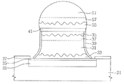
その際に、高温半田31内の、仕上げ層25又は導電性パッド23と接する領域に第1金属間化合物33が形成される。
高温半田31の水平幅は導電性パッド23に近くなるほど拡張される。高温半田31の側面は低温半田51の側面と異なる形状を有する。高温半田31の側面は前記バリア層45に近くなるほど導電性パッド23の上部表面に対して垂直に近いプロファイルを有する。高温半田31の側面は導電性パッド23に近くなるほど凹状のプロファイルを有する。
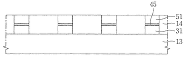
14 フィルム
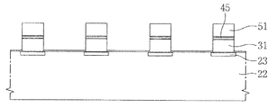
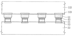
21、22、121、122 半導体パッケージ
23、123 導電性パッド
25、125 仕上げ層
27、127 パッケージ絶縁膜
31、131 高温半田
33、35、55、133、135、155 金属間化合物
37、57、137、157 拡散領域
39、139 側面酸化物
41、42、43、45、141、142、143、145 バリア層
51 低温半田
138 フラックス残渣
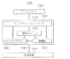
2100 電子システム
2110 ボディ
2120、2414 マイクロプロセッサ
2130 電源部
2140 機能ユニット
2150 ディスプレイコントローラ
2160 ディスプレイ
2170 外部装置
2180 通信ユニット
2400 電子システム
2412 メモリシステム
2416 RAM
2418 ユーザインタフェース
2420 バス
Claims (18)
- 導電性パッドと、
前記導電性パッド上に形成される高温半田と、
前記高温半田上に形成され、前記高温半田よりも低い融点を有する低温半田と、
前記高温半田と前記低温半田との間に形成されるバリア層と、を含み、
前記高温半田内のSn含有量が前記低温半田よりも高く、
前記高温半田の側面に形成された側面酸化物をさらに含むことを特徴とする半導体素子。 - 前記高温半田が純錫を含むことを特徴とする請求項1に記載の半導体素子。
- 前記高温半田が90wt%以上のSn含有量を有する混合物を含むことを特徴とする請求項1に記載の半導体素子。
- 前記低温半田がフラックスを含み、前記高温半田がフラックスを含まない、ことを特徴とする請求項1に記載の半導体素子。
- 前記側面酸化物がSnOを含むことを特徴とする請求項1に記載の半導体素子。
- 前記高温半田の側面が凹状(concave)のプロファイルを有し、前記低温半田の側面が凸状(convex)のプロファイルを有することを特徴とする請求項1に記載の半導体素子。
- 前記高温半田の側面のプロファイルは、前記バリア層に隣接する領域において、前記導電性パッドの上面に対して実質的に直線的かつ垂直であり、前記導電性パッドに隣接する領域において、凹状であることを特徴とする請求項1に記載の半導体素子。
- 前記高温半田の側面は、前記導電性パッドの上面に対して実質的に直線的かつ垂直なプロファイルを有し、前記低温半田の側面は、凸状のプロファイルを有することを特徴とする請求項1に記載の半導体素子。
- 前記バリア層と前記高温半田との間に第2金属間化合物(Inter−Metallic Compound)と、
前記バリア層と前記低温半田との間に第3金属間化合物と、をさらに含むことを特徴とする請求項1に記載の半導体素子。 - 前記バリア層は、
第1バリア層と、
前記第1バリア層下に形成される第2バリア層と、を含み、
前記第1バリア層は、前記第2バリア層よりも厚いことを特徴とする請求項9に記載の半導体素子。 - 前記第1バリア層は、ニッケル(Ni)を含み、前記第2バリア層は、ビスマス(Bi)を含むことを特徴とする請求項10に記載の半導体素子。
- 前記第2金属間化合物と前記高温半田との間に、第1拡散領域をさらに含み、
前記第1拡散領域は、前記第2バリア層及び前記高温半田の物質を含むことを特徴とする請求項10に記載の半導体素子。 - 前記第1バリア層上に形成される第3バリア層をさらに含み、
前記第1バリア層は、前記第2バリア層と前記第3バリア層との間に形成され、前記第3バリア層は、Biを含むことを特徴とする請求項10に記載の半導体素子。 - 前記第3金属間化合物と前記低温半田との間に形成される第2拡散領域をさらに含み、
前記第2拡散領域は、前記第3バリア層及び前記低温半田の物質を含むことを特徴とする請求項13に記載の半導体素子。 - 半導体パッケージの一面に形成される導電性パッドと、
前記導電性パッド上に形成される高温半田と、
前記高温半田上に形成され、前記高温半田よりも低い融点を有する低温半田と、
前記高温半田と前記低温半田との間に形成されるバリア層と、を含み、
前記高温半田の側面は、前記低温半田の側面と異なる形状を有し、
前記高温半田の側面は、凹状のプロファイルを有することを特徴とする半導体素子。 - 半導体パッケージの一面に形成される導電性パッドと、
前記導電性パッド上に形成される高温半田と、
前記高温半田上に形成され、前記高温半田よりも低い融点を有する低温半田と、
前記高温半田と前記低温半田との間に形成されるバリア層と、を含み、
前記高温半田の側面は、前記低温半田の側面と異なる形状を有し、
前記高温半田の側面のプロファイルは、前記バリア層に隣接する領域において、前記導電性パッドの上面に対して実質的に直線的かつ垂直であり、前記導電性パッドに隣接する領域において、凹状であることを特徴とする半導体素子。 - 半導体パッケージの一面に形成される導電性パッドと、
前記導電性パッド上に形成される高温半田と、
前記高温半田上に形成され、前記高温半田よりも低い融点を有する低温半田と、
前記高温半田と前記低温半田との間に形成されるバリア層と、を含み、
前記高温半田の側面は、前記低温半田の側面と異なる形状を有し、
前記低温半田の側面は、凸状のプロファイルを有することを特徴とする半導体素子。 - 半導体パッケージの一面に形成される導電性パッドと、
前記導電性パッド上に形成される高温半田と、
前記高温半田上に形成され、前記高温半田よりも低い融点を有する低温半田と、
前記高温半田と前記低温半田との間に形成されるバリア層と、を含み、
前記高温半田の側面は、前記低温半田の側面と異なる形状を有し、
前記高温半田の側面は、前記導電性パッドの上面に対して実質的に直線的かつ垂直のプロファイルを有することを特徴とする半導体素子。
Applications Claiming Priority (2)
| Application Number | Priority Date | Filing Date | Title |
|---|---|---|---|
| KR1020140095964A KR102192195B1 (ko) | 2014-07-28 | 2014-07-28 | 솔더 조인트를 갖는 반도체 소자 및 그 형성 방법 |
| KR10-2014-0095964 | 2014-07-28 |
Publications (3)
| Publication Number | Publication Date |
|---|---|
| JP2016032104A JP2016032104A (ja) | 2016-03-07 |
| JP2016032104A5 JP2016032104A5 (ja) | 2018-08-09 |
| JP6564261B2 true JP6564261B2 (ja) | 2019-08-21 |
Family
ID=55167330
Family Applications (1)
| Application Number | Title | Priority Date | Filing Date |
|---|---|---|---|
| JP2015136846A Active JP6564261B2 (ja) | 2014-07-28 | 2015-07-08 | 半田ジョイントを有する半導体素子 |
Country Status (3)
| Country | Link |
|---|---|
| US (1) | US9646945B2 (ja) |
| JP (1) | JP6564261B2 (ja) |
| KR (1) | KR102192195B1 (ja) |
Families Citing this family (10)
| Publication number | Priority date | Publication date | Assignee | Title |
|---|---|---|---|---|
| KR102601553B1 (ko) * | 2016-12-08 | 2023-11-15 | 삼성전자주식회사 | 반도체 발광 소자 |
| DE102017104276B4 (de) * | 2017-03-01 | 2020-01-16 | Osram Opto Semiconductors Gmbh | Verfahren zum Befestigen eines Halbleiterchips auf einem Leiterrahmen und elektronisches Bauelement |
| US10593638B2 (en) * | 2017-03-29 | 2020-03-17 | Xilinx, Inc. | Methods of interconnect for high density 2.5D and 3D integration |
| DE102017108422A1 (de) | 2017-04-20 | 2018-10-25 | Osram Opto Semiconductors Gmbh | Verfahren zum Befestigen eines Halbleiterchips auf einem Leiterrahmen und elektronisches Bauelement |
| US10403591B2 (en) * | 2017-10-31 | 2019-09-03 | Xilinx, Inc. | Chip package assembly with enhanced interconnects and method for fabricating the same |
| US10811377B2 (en) * | 2017-12-14 | 2020-10-20 | Taiwan Semiconductor Manufacturing Co., Ltd. | Package structure with a barrier layer and method for forming the same |
| US10453817B1 (en) | 2018-06-18 | 2019-10-22 | Texas Instruments Incorporated | Zinc-cobalt barrier for interface in solder bond applications |
| JP7721503B2 (ja) * | 2020-03-26 | 2025-08-12 | ローム株式会社 | 半導体装置 |
| KR102902359B1 (ko) * | 2020-09-22 | 2025-12-22 | 삼성전자주식회사 | 반도체 패키지 |
| US20250149486A1 (en) * | 2023-11-03 | 2025-05-08 | Taiwan Semiconductor Manufacturing Co., Ltd. | Semiconductor package and method of forming the same |
Family Cites Families (26)
| Publication number | Priority date | Publication date | Assignee | Title |
|---|---|---|---|---|
| US4739917A (en) * | 1987-01-12 | 1988-04-26 | Ford Motor Company | Dual solder process for connecting electrically conducting terminals of electrical components to printed circuit conductors |
| US5251806A (en) * | 1990-06-19 | 1993-10-12 | International Business Machines Corporation | Method of forming dual height solder interconnections |
| US5542174A (en) * | 1994-09-15 | 1996-08-06 | Intel Corporation | Method and apparatus for forming solder balls and solder columns |
| US5803343A (en) * | 1995-10-30 | 1998-09-08 | Delco Electronics Corp. | Solder process for enhancing reliability of multilayer hybrid circuits |
| US5803344A (en) * | 1996-09-09 | 1998-09-08 | Delco Electronics Corp. | Dual-solder process for enhancing reliability of thick-film hybrid circuits |
| US5953623A (en) * | 1997-04-10 | 1999-09-14 | International Business Machines Corporation | Ball limiting metal mask and tin enrichment of high melting point solder for low temperature interconnection |
| US5937320A (en) * | 1998-04-08 | 1999-08-10 | International Business Machines Corporation | Barrier layers for electroplated SnPb eutectic solder joints |
| US6483195B1 (en) * | 1999-03-16 | 2002-11-19 | Sumitomo Bakelite Company Limited | Transfer bump street, semiconductor flip chip and method of producing same |
| US6281106B1 (en) * | 1999-11-25 | 2001-08-28 | Delphi Technologies, Inc. | Method of solder bumping a circuit component |
| US6492197B1 (en) * | 2000-05-23 | 2002-12-10 | Unitive Electronics Inc. | Trilayer/bilayer solder bumps and fabrication methods therefor |
| US20030234276A1 (en) * | 2002-06-20 | 2003-12-25 | Ultratera Corporation | Strengthened bonding mechanism for semiconductor package |
| JP2004260157A (ja) * | 2003-02-07 | 2004-09-16 | Toshiba Corp | 半導体装置、半導体装置の製造方法及び組立方法 |
| US6893799B2 (en) | 2003-03-06 | 2005-05-17 | International Business Machines Corporation | Dual-solder flip-chip solder bump |
| JP2005011838A (ja) * | 2003-06-16 | 2005-01-13 | Toshiba Corp | 半導体装置及びその組立方法 |
| US7112524B2 (en) * | 2003-09-29 | 2006-09-26 | Phoenix Precision Technology Corporation | Substrate for pre-soldering material and fabrication method thereof |
| US20050199996A1 (en) | 2004-03-10 | 2005-09-15 | Ho Tony H. | Two solder array structure with two high melting solder joints |
| US20070036670A1 (en) | 2005-08-12 | 2007-02-15 | John Pereira | Solder composition |
| US20080248610A1 (en) | 2007-04-03 | 2008-10-09 | Advanpack Solutions Pte Ltd | Thermal bonding process for chip packaging |
| US8348139B2 (en) | 2010-03-09 | 2013-01-08 | Indium Corporation | Composite solder alloy preform |
| US8671560B2 (en) * | 2010-03-30 | 2014-03-18 | Research Triangle Institute | In system reflow of low temperature eutectic bond balls |
| KR101119839B1 (ko) * | 2010-05-23 | 2012-02-28 | 주식회사 네패스 | 범프 구조물 및 그 제조 방법 |
| JP2013534367A (ja) | 2010-08-02 | 2013-09-02 | アトテツク・ドイチユラント・ゲゼルシヤフト・ミツト・ベシユレンクテル・ハフツング | 基板上にはんだ堆積物および非溶融バンプを形成する方法 |
| JP6024079B2 (ja) * | 2011-08-18 | 2016-11-09 | 富士通株式会社 | 半導体装置およびその製造方法並びに電子装置 |
| TWI440518B (zh) | 2011-08-26 | 2014-06-11 | Univ Nat Taiwan Science Tech | 多層結構之高溫焊料及其製造方法 |
| US9368429B2 (en) * | 2011-10-25 | 2016-06-14 | Intel Corporation | Interposer for hermetic sealing of sensor chips and for their integration with integrated circuit chips |
| KR102007780B1 (ko) * | 2012-07-31 | 2019-10-21 | 삼성전자주식회사 | 멀티 범프 구조의 전기적 연결부를 포함하는 반도체 소자의 제조방법 |
-
2014
- 2014-07-28 KR KR1020140095964A patent/KR102192195B1/ko active Active
-
2015
- 2015-04-14 US US14/686,775 patent/US9646945B2/en active Active
- 2015-07-08 JP JP2015136846A patent/JP6564261B2/ja active Active
Also Published As
| Publication number | Publication date |
|---|---|
| JP2016032104A (ja) | 2016-03-07 |
| KR20160013737A (ko) | 2016-02-05 |
| KR102192195B1 (ko) | 2020-12-17 |
| US9646945B2 (en) | 2017-05-09 |
| US20160027751A1 (en) | 2016-01-28 |
Similar Documents
| Publication | Publication Date | Title |
|---|---|---|
| JP6564261B2 (ja) | 半田ジョイントを有する半導体素子 | |
| JP5435849B2 (ja) | 基板に取り付けられたスタッドバンプを伴う、フリップチップパッケージング用の可融性入出力相互接続システムおよび方法 | |
| JP5629580B2 (ja) | 二重ポスト付きフリップチップ相互接続 | |
| CN104900596B (zh) | 封装堆栈结构及其制法 | |
| CN102543939B (zh) | 超细间距焊盘的叠层倒装芯片封装结构及其制造方法 | |
| US20210210450A1 (en) | Semiconductor device and manufacturing method thereof | |
| KR20160019739A (ko) | 필라를 포함하는 반도체 소자 및 패키지 기판, 및 그것을 포함하는 반도체 패키지 및 패키지 적층 구조체 | |
| CN103201835A (zh) | 具有双重或多重蚀刻倒装芯片连接体的微电子封装和相应的制造方法 | |
| CN109427755B (zh) | 半导体装置组合件和其制造方法 | |
| TWI253697B (en) | Method for fabricating a flip chip package | |
| US11908820B2 (en) | Dual solder methodologies for ultrahigh density first level interconnections | |
| CN109390306A (zh) | 电子封装件 | |
| US20150155258A1 (en) | Method of fabricating a semiconductor structure having conductive bumps with a plurality of metal layers | |
| TWI799457B (zh) | 具有增進的互連之晶片封裝組件以及製造其之方法 | |
| JP2011171427A (ja) | 積層型半導体装置 | |
| US7679188B2 (en) | Semiconductor device having a bump formed over an electrode pad | |
| JP6729331B2 (ja) | 電子装置及び電子装置の製造方法 | |
| CN104584206B (zh) | 用于互连附着的迹线沾焊料技术 | |
| WO2017221587A1 (ja) | 基板装置、電子機器及び基板装置の製造方法 | |
| CN104201120A (zh) | 半导体倒装封装方法 | |
| US8698309B2 (en) | Semiconductor device | |
| CN104241236B (zh) | 一种半导体倒装封装结构 | |
| US9601374B2 (en) | Semiconductor die assembly | |
| JP6593119B2 (ja) | 電極構造、接合方法及び半導体装置 | |
| JP2006351589A (ja) | 半導体チップ、電子装置及びその製造方法 |
Legal Events
| Date | Code | Title | Description |
|---|---|---|---|
| A521 | Request for written amendment filed |
Free format text: JAPANESE INTERMEDIATE CODE: A523 Effective date: 20180629 |
|
| A621 | Written request for application examination |
Free format text: JAPANESE INTERMEDIATE CODE: A621 Effective date: 20180629 |
|
| A131 | Notification of reasons for refusal |
Free format text: JAPANESE INTERMEDIATE CODE: A131 Effective date: 20190319 |
|
| A521 | Request for written amendment filed |
Free format text: JAPANESE INTERMEDIATE CODE: A523 Effective date: 20190612 |
|
| TRDD | Decision of grant or rejection written | ||
| A01 | Written decision to grant a patent or to grant a registration (utility model) |
Free format text: JAPANESE INTERMEDIATE CODE: A01 Effective date: 20190709 |
|
| A61 | First payment of annual fees (during grant procedure) |
Free format text: JAPANESE INTERMEDIATE CODE: A61 Effective date: 20190726 |
|
| R150 | Certificate of patent or registration of utility model |
Ref document number: 6564261 Country of ref document: JP Free format text: JAPANESE INTERMEDIATE CODE: R150 |
|
| R250 | Receipt of annual fees |
Free format text: JAPANESE INTERMEDIATE CODE: R250 |
|
| R250 | Receipt of annual fees |
Free format text: JAPANESE INTERMEDIATE CODE: R250 |
|
| R250 | Receipt of annual fees |
Free format text: JAPANESE INTERMEDIATE CODE: R250 |
|
| R250 | Receipt of annual fees |
Free format text: JAPANESE INTERMEDIATE CODE: R250 |