JP6624698B2 - 画素配列構造、表示パネル及び表示装置 - Google Patents
画素配列構造、表示パネル及び表示装置 Download PDFInfo
- Publication number
- JP6624698B2 JP6624698B2 JP2017560851A JP2017560851A JP6624698B2 JP 6624698 B2 JP6624698 B2 JP 6624698B2 JP 2017560851 A JP2017560851 A JP 2017560851A JP 2017560851 A JP2017560851 A JP 2017560851A JP 6624698 B2 JP6624698 B2 JP 6624698B2
- Authority
- JP
- Japan
- Prior art keywords
- pixel
- sub
- pixels
- green
- adjacent
- Prior art date
- Legal status (The legal status is an assumption and is not a legal conclusion. Google has not performed a legal analysis and makes no representation as to the accuracy of the status listed.)
- Active
Links
Images




Classifications
-
- G—PHYSICS
- G02—OPTICS
- G02F—OPTICAL DEVICES OR ARRANGEMENTS FOR THE CONTROL OF LIGHT BY MODIFICATION OF THE OPTICAL PROPERTIES OF THE MEDIA OF THE ELEMENTS INVOLVED THEREIN; NON-LINEAR OPTICS; FREQUENCY-CHANGING OF LIGHT; OPTICAL LOGIC ELEMENTS; OPTICAL ANALOGUE/DIGITAL CONVERTERS
- G02F1/00—Devices or arrangements for the control of the intensity, colour, phase, polarisation or direction of light arriving from an independent light source, e.g. switching, gating or modulating; Non-linear optics
- G02F1/01—Devices or arrangements for the control of the intensity, colour, phase, polarisation or direction of light arriving from an independent light source, e.g. switching, gating or modulating; Non-linear optics for the control of the intensity, phase, polarisation or colour
- G02F1/13—Devices or arrangements for the control of the intensity, colour, phase, polarisation or direction of light arriving from an independent light source, e.g. switching, gating or modulating; Non-linear optics for the control of the intensity, phase, polarisation or colour based on liquid crystals, e.g. single liquid crystal display cells
- G02F1/133—Constructional arrangements; Operation of liquid crystal cells; Circuit arrangements
- G02F1/1333—Constructional arrangements; Manufacturing methods
- G02F1/1343—Electrodes
- G02F1/134309—Electrodes characterised by their geometrical arrangement
- G02F1/134336—Matrix
-
- G—PHYSICS
- G02—OPTICS
- G02F—OPTICAL DEVICES OR ARRANGEMENTS FOR THE CONTROL OF LIGHT BY MODIFICATION OF THE OPTICAL PROPERTIES OF THE MEDIA OF THE ELEMENTS INVOLVED THEREIN; NON-LINEAR OPTICS; FREQUENCY-CHANGING OF LIGHT; OPTICAL LOGIC ELEMENTS; OPTICAL ANALOGUE/DIGITAL CONVERTERS
- G02F1/00—Devices or arrangements for the control of the intensity, colour, phase, polarisation or direction of light arriving from an independent light source, e.g. switching, gating or modulating; Non-linear optics
- G02F1/01—Devices or arrangements for the control of the intensity, colour, phase, polarisation or direction of light arriving from an independent light source, e.g. switching, gating or modulating; Non-linear optics for the control of the intensity, phase, polarisation or colour
- G02F1/13—Devices or arrangements for the control of the intensity, colour, phase, polarisation or direction of light arriving from an independent light source, e.g. switching, gating or modulating; Non-linear optics for the control of the intensity, phase, polarisation or colour based on liquid crystals, e.g. single liquid crystal display cells
- G02F1/133—Constructional arrangements; Operation of liquid crystal cells; Circuit arrangements
- G02F1/1333—Constructional arrangements; Manufacturing methods
- G02F1/1335—Structural association of cells with optical devices, e.g. polarisers or reflectors
-
- G—PHYSICS
- G02—OPTICS
- G02F—OPTICAL DEVICES OR ARRANGEMENTS FOR THE CONTROL OF LIGHT BY MODIFICATION OF THE OPTICAL PROPERTIES OF THE MEDIA OF THE ELEMENTS INVOLVED THEREIN; NON-LINEAR OPTICS; FREQUENCY-CHANGING OF LIGHT; OPTICAL LOGIC ELEMENTS; OPTICAL ANALOGUE/DIGITAL CONVERTERS
- G02F1/00—Devices or arrangements for the control of the intensity, colour, phase, polarisation or direction of light arriving from an independent light source, e.g. switching, gating or modulating; Non-linear optics
- G02F1/01—Devices or arrangements for the control of the intensity, colour, phase, polarisation or direction of light arriving from an independent light source, e.g. switching, gating or modulating; Non-linear optics for the control of the intensity, phase, polarisation or colour
- G02F1/13—Devices or arrangements for the control of the intensity, colour, phase, polarisation or direction of light arriving from an independent light source, e.g. switching, gating or modulating; Non-linear optics for the control of the intensity, phase, polarisation or colour based on liquid crystals, e.g. single liquid crystal display cells
- G02F1/133—Constructional arrangements; Operation of liquid crystal cells; Circuit arrangements
- G02F1/1333—Constructional arrangements; Manufacturing methods
- G02F1/1343—Electrodes
- G02F1/134309—Electrodes characterised by their geometrical arrangement
-
- G—PHYSICS
- G02—OPTICS
- G02F—OPTICAL DEVICES OR ARRANGEMENTS FOR THE CONTROL OF LIGHT BY MODIFICATION OF THE OPTICAL PROPERTIES OF THE MEDIA OF THE ELEMENTS INVOLVED THEREIN; NON-LINEAR OPTICS; FREQUENCY-CHANGING OF LIGHT; OPTICAL LOGIC ELEMENTS; OPTICAL ANALOGUE/DIGITAL CONVERTERS
- G02F1/00—Devices or arrangements for the control of the intensity, colour, phase, polarisation or direction of light arriving from an independent light source, e.g. switching, gating or modulating; Non-linear optics
- G02F1/01—Devices or arrangements for the control of the intensity, colour, phase, polarisation or direction of light arriving from an independent light source, e.g. switching, gating or modulating; Non-linear optics for the control of the intensity, phase, polarisation or colour
- G02F1/13—Devices or arrangements for the control of the intensity, colour, phase, polarisation or direction of light arriving from an independent light source, e.g. switching, gating or modulating; Non-linear optics for the control of the intensity, phase, polarisation or colour based on liquid crystals, e.g. single liquid crystal display cells
- G02F1/133—Constructional arrangements; Operation of liquid crystal cells; Circuit arrangements
- G02F1/1333—Constructional arrangements; Manufacturing methods
- G02F1/1343—Electrodes
- G02F1/13439—Electrodes characterised by their electrical, optical, physical properties; materials therefor; method of making
-
- G—PHYSICS
- G02—OPTICS
- G02F—OPTICAL DEVICES OR ARRANGEMENTS FOR THE CONTROL OF LIGHT BY MODIFICATION OF THE OPTICAL PROPERTIES OF THE MEDIA OF THE ELEMENTS INVOLVED THEREIN; NON-LINEAR OPTICS; FREQUENCY-CHANGING OF LIGHT; OPTICAL LOGIC ELEMENTS; OPTICAL ANALOGUE/DIGITAL CONVERTERS
- G02F1/00—Devices or arrangements for the control of the intensity, colour, phase, polarisation or direction of light arriving from an independent light source, e.g. switching, gating or modulating; Non-linear optics
- G02F1/01—Devices or arrangements for the control of the intensity, colour, phase, polarisation or direction of light arriving from an independent light source, e.g. switching, gating or modulating; Non-linear optics for the control of the intensity, phase, polarisation or colour
- G02F1/13—Devices or arrangements for the control of the intensity, colour, phase, polarisation or direction of light arriving from an independent light source, e.g. switching, gating or modulating; Non-linear optics for the control of the intensity, phase, polarisation or colour based on liquid crystals, e.g. single liquid crystal display cells
- G02F1/133—Constructional arrangements; Operation of liquid crystal cells; Circuit arrangements
- G02F1/136—Liquid crystal cells structurally associated with a semi-conducting layer or substrate, e.g. cells forming part of an integrated circuit
- G02F1/1362—Active matrix addressed cells
- G02F1/1368—Active matrix addressed cells in which the switching element is a three-electrode device
-
- H—ELECTRICITY
- H10—SEMICONDUCTOR DEVICES; ELECTRIC SOLID-STATE DEVICES NOT OTHERWISE PROVIDED FOR
- H10K—ORGANIC ELECTRIC SOLID-STATE DEVICES
- H10K59/00—Integrated devices, or assemblies of multiple devices, comprising at least one organic light-emitting element covered by group H10K50/00
- H10K59/30—Devices specially adapted for multicolour light emission
- H10K59/35—Devices specially adapted for multicolour light emission comprising red-green-blue [RGB] subpixels
- H10K59/353—Devices specially adapted for multicolour light emission comprising red-green-blue [RGB] subpixels characterised by the geometrical arrangement of the RGB subpixels
-
- G—PHYSICS
- G02—OPTICS
- G02F—OPTICAL DEVICES OR ARRANGEMENTS FOR THE CONTROL OF LIGHT BY MODIFICATION OF THE OPTICAL PROPERTIES OF THE MEDIA OF THE ELEMENTS INVOLVED THEREIN; NON-LINEAR OPTICS; FREQUENCY-CHANGING OF LIGHT; OPTICAL LOGIC ELEMENTS; OPTICAL ANALOGUE/DIGITAL CONVERTERS
- G02F1/00—Devices or arrangements for the control of the intensity, colour, phase, polarisation or direction of light arriving from an independent light source, e.g. switching, gating or modulating; Non-linear optics
- G02F1/01—Devices or arrangements for the control of the intensity, colour, phase, polarisation or direction of light arriving from an independent light source, e.g. switching, gating or modulating; Non-linear optics for the control of the intensity, phase, polarisation or colour
- G02F1/13—Devices or arrangements for the control of the intensity, colour, phase, polarisation or direction of light arriving from an independent light source, e.g. switching, gating or modulating; Non-linear optics for the control of the intensity, phase, polarisation or colour based on liquid crystals, e.g. single liquid crystal display cells
- G02F1/133—Constructional arrangements; Operation of liquid crystal cells; Circuit arrangements
- G02F1/1333—Constructional arrangements; Manufacturing methods
- G02F1/1343—Electrodes
- G02F1/134309—Electrodes characterised by their geometrical arrangement
- G02F1/134345—Subdivided pixels, e.g. for grey scale or redundancy
-
- G—PHYSICS
- G02—OPTICS
- G02F—OPTICAL DEVICES OR ARRANGEMENTS FOR THE CONTROL OF LIGHT BY MODIFICATION OF THE OPTICAL PROPERTIES OF THE MEDIA OF THE ELEMENTS INVOLVED THEREIN; NON-LINEAR OPTICS; FREQUENCY-CHANGING OF LIGHT; OPTICAL LOGIC ELEMENTS; OPTICAL ANALOGUE/DIGITAL CONVERTERS
- G02F2201/00—Constructional arrangements not provided for in groups G02F1/00 - G02F7/00
- G02F2201/52—RGB geometrical arrangements
Landscapes
- Physics & Mathematics (AREA)
- Nonlinear Science (AREA)
- Mathematical Physics (AREA)
- Chemical & Material Sciences (AREA)
- Crystallography & Structural Chemistry (AREA)
- General Physics & Mathematics (AREA)
- Optics & Photonics (AREA)
- Geometry (AREA)
- Engineering & Computer Science (AREA)
- Microelectronics & Electronic Packaging (AREA)
- Devices For Indicating Variable Information By Combining Individual Elements (AREA)
- Electroluminescent Light Sources (AREA)
- Liquid Crystal (AREA)
Description
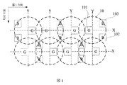
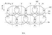
101:緑色副画素
102:赤色副画素
103:青色副画素
Claims (18)
- 複数の第1副画素、複数の第2副画素及び複数の第3副画素を含む画素配列構造において、
各画素に1つの第1副画素が含まれ、各第2副画素と各第3副画素は、それぞれ隣接する少なくとも2つの画素により共用され、
画素アレイの第1方向で、副画素密度が画素密度の1.5倍であり、
画素アレイの前記第1方向とは異なる第2方向で、副画素密度が画素密度の1.5倍であり、
前記第1副画素は、緑色副画素であり、前記第2副画素は、赤色副画素であり、前記第3副画素は、青色副画素であり、
前記第1方向と前記第2方向で、前記緑色副画素が、2つずつが隣接してペアになるように設置され、
前記第2方向での任意の接近する2ペアの前記緑色副画素の間に1つの前記青色副画素が設置され、
前記青色副画素が、2つずつが隣接するように設置される
ことを特徴とする画素配列構造。 - 前記第1方向は、水平方向であり、
前記第2方向は、縦方向であることを特徴とする請求項1に記載の画素配列構造。 - 前記第1方向での任意の接近する2ペアの前記緑色副画素の間に1つの赤色副画素が設置されることを特徴とする請求項1に記載の画素配列構造。
- 隣接して設置される2つの前記青色副画素は、一体化され、1つの駆動回路により駆動される特徴とする請求項1に記載の画素配列構造。
- 前記第1方向は、水平方向であり、前記第2方向は、縦方向であり、
画素アレイの奇数行で、任意のペアの前記緑色副画素は、それぞれ水平仮想直線の両側に位置し、接近する2ペアの前記緑色副画素の間に位置する赤色副画素とその両側の前記緑色副画素は、前記水平仮想直線の同一側に位置し、
画素アレイの偶数行で、任意のペアの前記緑色副画素は、前記水平仮想直線の同一側に位置し、且つ任意の接近する2ペアの前記緑色副画素は、前記水平仮想直線の両側に位置し、接近する2ペアの前記緑色副画素の間に位置する赤色副画素は、前記水平仮想直線の上に位置し、
画素アレイの各列で、任意のペアの前記緑色副画素は、それぞれ縦仮想直線の両側に位置し、且つ、接近する2ペアの前記緑色副画素の間に位置する青色副画素と、同一の画素に属する前記緑色副画素は、前記縦仮想直線の同一側に位置することを特徴とする請求項3に記載の画素配列構造。 - 複数の第1副画素、複数の第2副画素及び複数の第3副画素を含む画素配列構造において、
各画素に1つの第1副画素が含まれ、各第2副画素と各第3副画素は、それぞれ隣接する少なくとも2つの画素により共用され、
画素アレイの第1方向で、副画素密度が画素密度の1.5倍であり、画素アレイの第2方向で、副画素密度が画素密度の1.5倍であり、
前記第1方向は、水平方向であり、前記第2方向は、縦方向であり、
前記第1副画素は、緑色副画素であり、前記第2副画素は、赤色副画素であり、前記第3副画素は、青色副画素であり、
前記第1方向と前記第2方向で、前記緑色副画素が、2つずつが隣接してペアになるように設置されることにより、緑色含画素ペアが構成され、
前記第1方向での任意の接近する2ペアの前記緑色副画素の間に1つの前記青色副画素と1つの前記赤色副画素が設置され、
1つの前記青色副画素と1つの前記赤色副画素は、前記第2方向で配列され、
画素アレイの各行で、すべての前記緑色副画素は、いずれも水平仮想直線上に位置し、
画素アレイの各列で、1つの緑色含画素ペアを構成する2つの前記緑色副画素は、縦仮想直線の両側に位置し、
前記赤色副画素と前記青色副画素は、隣接する2本の前記縦仮想直線の間に位置し、且つそれぞれ前記水平仮想直線の両側に位置する
ことを特徴とする画素配列構造。 - 複数の前記水平仮想直線と複数の前記縦仮想直線は、画素アレイのグリッドラインを構成することを特徴とする請求項6に記載の画素配列構造。
- 複数の第1副画素、複数の第2副画素及び複数の第3副画素を含む画素配列構造において、
各画素に1つの第1副画素が含まれ、各第2副画素と各第3副画素は、それぞれ隣接する少なくとも2つの画素により共用され、
画素アレイの第1方向で、副画素密度が画素密度の1.5倍であり、画素アレイの第2方向で、副画素密度が画素密度の1.5倍であり、
前記第1方向は、前記第2方向と直交し、
前記第1副画素は、緑色副画素であり、前記第2副画素は、赤色副画素であり、前記第3副画素は、青色副画素であり、
前記第1方向で、前記緑色副画素が、2つずつが隣接してペアになるように設置されることにより、緑色副画素ペアが構成され、
前記第1方向での任意の接近する2つの緑色副画素ペアの間に1つの前記青色副画素と1つの前記赤色副画素が設置されることにより、1つの混合副画素ペアが構成され、
前記1つの混合副画素ペアを構成する1つの前記青色副画素と1つの前記赤色副画素は、前記第2方向で配列される
ことを特徴とする画素配列構造。 - 前記第1方向で、2つずつが隣接して緑色副画素ペアを構成するように設置される2つの前記緑色副画素が、第1方向に沿って伸びる第1仮想直線上に位置し、
前記第2方向で、前記第1方向での任意の接近する2つの緑色副画素ペアの間に設置される混合副画素ペアは、第2方向に沿って伸びる2本の隣接する第2仮想直線の間に位置し、
前記2つの緑色副画素ペアのうちの1つの緑色副画素ペアと前記混合副画素ペアは、前記2本の隣接する第2仮想直線のうちの1本の第2仮想直線の両側に位置し、
前記2つの緑色副画素ペアのうちのもう1つの緑色副画素ペアと前記混合副画素ペアは、前記2本の隣接する第2仮想直線のうちのもう1本の第2仮想直線の両側に位置し、
複数の第1仮想直線と複数の第2仮想直線は、画素アレイのグリッドラインを構成することを特徴とする請求項8に記載の画素配列構造。 - 前記第1方向での1つの緑色副画素ペアを構成する2つの緑色副画素の間に、間隔があいており、
前記2つの緑色副画素の発光層が連結されることを特徴とする請求項6又は8に記載の画素配列構造。 - 前記第1方向で2つずつが隣接してペアになるように設置される2つの緑色副画素の間に、他の副画素が挟まれないことを特徴とする請求項6〜10のいずれか一項に記載の画素配列構造。
- 前記第1方向での1つの緑色副画素ペアを構成する2つの緑色副画素の間隔は、第1方向での任意の接近する2つの緑色副画素ペアの間隔より小さいことを特徴とする請求項11に記載の画素配列構造。
- 複数の第1副画素、複数の第2副画素及び複数の第3副画素を含む画素配列構造において、
各画素に1つの第1副画素が含まれ、各第2副画素と各第3副画素は、それぞれ隣接する少なくとも2つの画素により共用され、
画素アレイの第1方向で、副画素密度が画素密度の1.5倍であり、
画素アレイの前記第1方向とは異なる第2方向で、副画素密度が画素密度の1.5倍であり、
前記第1副画素は、緑色副画素であり、前記第2副画素は、赤色副画素であり、前記第3副画素は、青色副画素であり、
前記第1方向で、前記緑色副画素が、2つずつが隣接してペアになるように設置され、
前記第1方向での任意の接近する2ペアの緑色副画素の間に、2つの青色副画素又は2つの赤色副画素が設置され、
前記第2方向で、前記赤色副画素が、2つずつが隣接してペアになるように設置され、前記青色副画素が、2つずつが隣接してペアになるように設置され、
前記第1方向での任意のペアの前記緑色副画素は、2ペアの前記赤色副画素と、2ペアの前記青色副画素により囲まれる
ことを特徴とする画素配列構造。 - ペアになって設置される2つの前記青色副画素は、一体化され、1つの駆動回路により駆動されることを特徴とする請求項13に記載の画素配列構造。
- ペアになって設置される2つの前記赤色副画素は、一体化され、1つの駆動回路により駆動されることを特徴とする請求項13又は14に記載の画素配列構造。
- 前記第1方向は、水平方向であり、前記第2方向は、縦方向であり、
画素アレイの各行で、すべての前記緑色副画素は、いずれも水平仮想直線の上に位置し、
画素アレイの各列で、任意の隣接する2つの前記緑色副画素は、縦仮想直線の両側に位置し、
各ペアの前記赤色副画素は、隣接する2本の前記縦仮想直線の間に位置し、且つ、それぞれ偶数行の前記水平仮想直線の両側に位置し、各ペアの青色副画素は、隣接する2本の前記縦仮想直線の間に位置し、且つそれぞれ奇数行の前記水平仮想直線の両側に位置することを特徴とする請求項13に記載の画素配列構造。 - 表示パネルの画素が、請求項1〜16のいずれか一項に記載する画素配列構造により配列して構成される表示パネル。
- 請求項17に記載の表示パネルを含む表示装置。
Applications Claiming Priority (3)
| Application Number | Priority Date | Filing Date | Title |
|---|---|---|---|
| CN201510080570.0 | 2015-02-13 | ||
| CN201510080570.0A CN104597655B (zh) | 2015-02-13 | 2015-02-13 | 一种像素排列结构、显示面板及显示装置 |
| PCT/CN2015/085510 WO2016127593A1 (zh) | 2015-02-13 | 2015-07-30 | 一种像素排列结构、显示面板及显示装置 |
Publications (2)
| Publication Number | Publication Date |
|---|---|
| JP2018512627A JP2018512627A (ja) | 2018-05-17 |
| JP6624698B2 true JP6624698B2 (ja) | 2019-12-25 |
Family
ID=53123546
Family Applications (1)
| Application Number | Title | Priority Date | Filing Date |
|---|---|---|---|
| JP2017560851A Active JP6624698B2 (ja) | 2015-02-13 | 2015-07-30 | 画素配列構造、表示パネル及び表示装置 |
Country Status (6)
| Country | Link |
|---|---|
| US (1) | US9946123B2 (ja) |
| EP (1) | EP3270216B1 (ja) |
| JP (1) | JP6624698B2 (ja) |
| KR (1) | KR101755271B1 (ja) |
| CN (1) | CN104597655B (ja) |
| WO (1) | WO2016127593A1 (ja) |
Families Citing this family (51)
| Publication number | Priority date | Publication date | Assignee | Title |
|---|---|---|---|---|
| CN104375302B (zh) * | 2014-10-27 | 2020-09-08 | 上海中航光电子有限公司 | 一种像素结构、显示面板及其像素补偿方法 |
| CN104597655B (zh) | 2015-02-13 | 2017-06-27 | 京东方科技集团股份有限公司 | 一种像素排列结构、显示面板及显示装置 |
| CN106486514B (zh) * | 2015-08-31 | 2023-12-01 | 昆山国显光电有限公司 | 像素结构以及oled显示面板 |
| CN105304678B (zh) * | 2015-09-25 | 2018-11-16 | 上海和辉光电有限公司 | 有机发光二极管显示面板的像素排列结构及掩膜板 |
| US11233096B2 (en) | 2016-02-18 | 2022-01-25 | Boe Technology Group Co., Ltd. | Pixel arrangement structure and driving method thereof, display substrate and display device |
| CN205355055U (zh) * | 2016-02-18 | 2016-06-29 | 京东方科技集团股份有限公司 | 一种像素排列结构、显示面板及显示装置 |
| WO2021016946A1 (zh) | 2019-07-31 | 2021-02-04 | 京东方科技集团股份有限公司 | 显示基板及其制备方法、显示面板、显示装置 |
| US11747531B2 (en) | 2016-02-18 | 2023-09-05 | Chengdu Boe Optoelectronics Technology Co., Ltd. | Display substrate, fine metal mask set and manufacturing method thereof |
| US11448807B2 (en) | 2016-02-18 | 2022-09-20 | Chengdu Boe Optoelectronics Technology Co., Ltd. | Display substrate, fine metal mask set and manufacturing method thereof |
| CN107644888B (zh) * | 2016-07-22 | 2025-01-10 | 京东方科技集团股份有限公司 | 像素排列结构、显示基板、显示装置、制作方法及掩膜版 |
| US10854684B2 (en) | 2016-02-18 | 2020-12-01 | Boe Technology Group Co., Ltd. | Pixel arrangement structure and driving method thereof, display substrate and display device |
| CN110137213B (zh) | 2018-02-09 | 2025-03-25 | 京东方科技集团股份有限公司 | 像素排列结构及其显示方法、显示基板 |
| CN110133899A (zh) | 2018-02-09 | 2019-08-16 | 京东方科技集团股份有限公司 | 像素排列结构、显示基板、显示装置 |
| CN110137215B (zh) | 2018-02-09 | 2025-01-14 | 京东方科技集团股份有限公司 | 像素排列结构、显示基板和显示装置 |
| CN110134353B (zh) | 2018-02-09 | 2021-04-27 | 京东方科技集团股份有限公司 | 颜色补偿方法、补偿装置以及显示装置 |
| US11264430B2 (en) | 2016-02-18 | 2022-03-01 | Chengdu Boe Optoelectronics Technology Co., Ltd. | Pixel arrangement structure with misaligned repeating units, display substrate, display apparatus and method of fabrication thereof |
| US10600213B2 (en) * | 2016-02-27 | 2020-03-24 | Focal Sharp, Inc. | Method and apparatus for color-preserving spectrum reshape |
| CN107275359B (zh) | 2016-04-08 | 2021-08-13 | 乐金显示有限公司 | 有机发光显示装置 |
| KR102692417B1 (ko) * | 2016-04-29 | 2024-08-05 | 엘지디스플레이 주식회사 | 유기 발광 표시 장치 |
| KR101698718B1 (ko) * | 2016-04-29 | 2017-01-20 | 엘지디스플레이 주식회사 | 유기 발광 표시 장치 |
| CN107887404B (zh) * | 2016-09-29 | 2020-04-07 | 昆山国显光电有限公司 | Amoled像素结构及显示装置 |
| CN107221555B (zh) * | 2017-06-21 | 2019-02-26 | 深圳市华星光电半导体显示技术有限公司 | Oled显示面板以及显示装置 |
| CN107731093B (zh) * | 2017-09-12 | 2019-08-20 | 维沃移动通信有限公司 | 一种像素排列结构、显示面板及移动终端 |
| WO2019062236A1 (zh) | 2017-09-30 | 2019-04-04 | 昆山国显光电有限公司 | 显示屏、显示屏驱动方法及其显示装置 |
| WO2019062221A1 (zh) * | 2017-09-30 | 2019-04-04 | 云谷(固安)科技有限公司 | 显示屏及显示装置 |
| CN108269840B (zh) * | 2017-09-30 | 2021-08-13 | 昆山国显光电有限公司 | 显示屏及显示装置 |
| CN108364967B (zh) * | 2017-09-30 | 2021-07-27 | 昆山国显光电有限公司 | 显示屏及显示装置 |
| CN108461521A (zh) * | 2017-09-30 | 2018-08-28 | 昆山国显光电有限公司 | 显示屏及显示装置 |
| CN114994973B (zh) | 2018-02-09 | 2023-04-28 | 京东方科技集团股份有限公司 | 显示基板和显示装置 |
| CN110137212B (zh) * | 2018-02-09 | 2022-05-27 | 京东方科技集团股份有限公司 | 像素排列结构、显示基板以及显示装置 |
| US11574960B2 (en) | 2018-02-09 | 2023-02-07 | Boe Technology Group Co., Ltd. | Pixel arrangement structure, display substrate, display device and mask plate group |
| CN109037302A (zh) * | 2018-09-13 | 2018-12-18 | 武汉华星光电半导体显示技术有限公司 | 像素排列结构及显示装置 |
| CN113823240B (zh) | 2018-12-13 | 2023-04-18 | 京东方科技集团股份有限公司 | 显示装置 |
| CN110288946B (zh) * | 2019-06-25 | 2021-10-15 | 荣耀终端有限公司 | 移动终端及其驱动方法、显示模组、驱动芯片 |
| CN110189683A (zh) * | 2019-06-26 | 2019-08-30 | 京东方科技集团股份有限公司 | 一种显示面板、其驱动方法及显示装置 |
| CN112673476B (zh) | 2019-07-31 | 2025-12-30 | 京东方科技集团股份有限公司 | 显示基板和显示装置 |
| KR20210016141A (ko) * | 2019-07-31 | 2021-02-15 | 삼성디스플레이 주식회사 | 디스플레이 패널 |
| US11367377B2 (en) * | 2019-08-02 | 2022-06-21 | Tianma Japan, Ltd. | Display device |
| JP7572160B2 (ja) * | 2019-08-02 | 2024-10-23 | Tianma Japan株式会社 | 表示装置 |
| US12266303B2 (en) | 2019-08-23 | 2025-04-01 | Boe Technology Group Co., Ltd. | Display device and manufacturing method thereof |
| CN112840461B (zh) | 2019-08-23 | 2025-02-25 | 京东方科技集团股份有限公司 | 显示面板及其制造方法、显示装置 |
| EP4020449B1 (en) | 2019-08-23 | 2025-06-25 | BOE Technology Group Co., Ltd. | Display device and manufacturing method thereof |
| CN112703604B (zh) | 2019-08-23 | 2024-06-18 | 京东方科技集团股份有限公司 | 显示装置及其制备方法 |
| CN110580872B (zh) * | 2019-09-29 | 2022-08-26 | 武汉天马微电子有限公司 | 一种显示面板和显示装置 |
| CN112649994B (zh) * | 2020-12-28 | 2022-09-13 | 视涯科技股份有限公司 | 阵列基板的设计方法、阵列基板、显示面板及显示装置 |
| CN112817187A (zh) * | 2021-02-05 | 2021-05-18 | 武汉华星光电技术有限公司 | 显示面板及显示装置 |
| US20240206272A1 (en) * | 2021-03-16 | 2024-06-20 | Boe Technology Group Co., Ltd. | Array substrate and display device |
| KR102876468B1 (ko) | 2021-03-23 | 2025-10-27 | 삼성디스플레이 주식회사 | 표시 장치 |
| CN114360443B (zh) * | 2021-11-30 | 2023-06-06 | 深圳市洲明科技股份有限公司 | 子像素渲染方法、装置和计算机设备 |
| CN114879397B (zh) * | 2022-05-23 | 2023-05-09 | 重庆惠科金渝光电科技有限公司 | 显示面板、显示面板的驱动方法和显示装置 |
| CN117672123B (zh) * | 2023-12-11 | 2025-11-11 | 佛山市国星光电股份有限公司 | 次级像素排布结构、虚拟像素排布结构及复用控制方法 |
Family Cites Families (22)
| Publication number | Priority date | Publication date | Assignee | Title |
|---|---|---|---|---|
| JPS60120398A (ja) | 1983-12-02 | 1985-06-27 | シチズン時計株式会社 | マトリクス形カラー表示装置の駆動方法 |
| JP3547015B2 (ja) * | 1993-01-07 | 2004-07-28 | ソニー株式会社 | 画像表示装置および画像表示装置の解像度改善方法 |
| JP2005091875A (ja) * | 2003-09-18 | 2005-04-07 | Nippon Hoso Kyokai <Nhk> | 表示装置及び表示方法 |
| CN100478757C (zh) * | 2004-08-05 | 2009-04-15 | 奇美电子股份有限公司 | 彩色滤光装置、显示方法及其应用 |
| US7907133B2 (en) * | 2006-04-13 | 2011-03-15 | Daktronics, Inc. | Pixel interleaving configurations for use in high definition electronic sign displays |
| JP4721460B2 (ja) * | 2007-02-02 | 2011-07-13 | キヤノン株式会社 | 表示装置及びその製造方法 |
| US8330152B2 (en) * | 2009-12-02 | 2012-12-11 | Universal Display Corporation | OLED display architecture with improved aperture ratio |
| US9041625B2 (en) | 2010-04-21 | 2015-05-26 | Lg Display Co., Ltd. | Subpixel arrangement structure for a display device and display device |
| KR101189025B1 (ko) * | 2010-05-31 | 2012-10-08 | 삼성디스플레이 주식회사 | 유기전계발광 표시장치의 화소배열구조 |
| CN103185995B (zh) * | 2011-12-30 | 2016-03-16 | 上海中航光电子有限公司 | 一种双栅极驱动的横向排列的像素结构及液晶显示装置 |
| KR101615332B1 (ko) | 2012-03-06 | 2016-04-26 | 삼성디스플레이 주식회사 | 유기 발광 표시 장치의 화소 배열 구조 |
| KR102063973B1 (ko) * | 2012-09-12 | 2020-01-09 | 삼성디스플레이 주식회사 | 유기전계발광 표시장치 및 그의 구동방법 |
| EP3780113B1 (en) | 2012-09-13 | 2025-07-16 | Samsung Display Co., Ltd. | Pixel arrangement structure for organic light emitting diode display |
| US20140111115A1 (en) * | 2012-10-22 | 2014-04-24 | Motorola Mobility Llc | Display devices having non-uniform sub-pixel spacing and methods therefor |
| CN103278960B (zh) * | 2012-12-31 | 2015-11-25 | 上海天马微电子有限公司 | 一种三色像素结构、彩膜基板及液晶显示器 |
| KR102030799B1 (ko) * | 2013-03-11 | 2019-10-11 | 삼성디스플레이 주식회사 | 유기발광표시장치 |
| CN104282230B (zh) * | 2013-07-10 | 2017-04-05 | 上海和辉光电有限公司 | 像素阵列及具有该像素阵列的平面显示器 |
| CN103325315B (zh) * | 2013-07-10 | 2015-09-16 | 上海和辉光电有限公司 | 像素阵列及具有该像素阵列的显示器 |
| US9262961B2 (en) | 2013-08-30 | 2016-02-16 | Au Optronics Corporation | Pixel arrangement of color display apparatus |
| CN104037202B (zh) * | 2014-06-12 | 2017-08-04 | 上海和辉光电有限公司 | 一种amoled显示器件及其子像素结构的制备方法 |
| CN104282727B (zh) * | 2014-09-30 | 2017-08-29 | 京东方科技集团股份有限公司 | 一种像素结构及其显示方法、显示装置 |
| CN104597655B (zh) * | 2015-02-13 | 2017-06-27 | 京东方科技集团股份有限公司 | 一种像素排列结构、显示面板及显示装置 |
-
2015
- 2015-02-13 CN CN201510080570.0A patent/CN104597655B/zh active Active
- 2015-07-30 JP JP2017560851A patent/JP6624698B2/ja active Active
- 2015-07-30 US US14/917,200 patent/US9946123B2/en active Active
- 2015-07-30 EP EP15837127.8A patent/EP3270216B1/en active Active
- 2015-07-30 WO PCT/CN2015/085510 patent/WO2016127593A1/zh not_active Ceased
- 2015-07-30 KR KR1020167005052A patent/KR101755271B1/ko active Active
Also Published As
| Publication number | Publication date |
|---|---|
| US20160357076A1 (en) | 2016-12-08 |
| JP2018512627A (ja) | 2018-05-17 |
| EP3270216B1 (en) | 2024-02-21 |
| US9946123B2 (en) | 2018-04-17 |
| KR101755271B1 (ko) | 2017-07-07 |
| EP3270216A4 (en) | 2018-12-12 |
| KR20160111899A (ko) | 2016-09-27 |
| EP3270216A1 (en) | 2018-01-17 |
| CN104597655B (zh) | 2017-06-27 |
| WO2016127593A1 (zh) | 2016-08-18 |
| CN104597655A (zh) | 2015-05-06 |
Similar Documents
| Publication | Publication Date | Title |
|---|---|---|
| JP6624698B2 (ja) | 画素配列構造、表示パネル及び表示装置 | |
| CN108701708B (zh) | 像素排列结构、显示面板及显示装置 | |
| CN110133919B (zh) | 显示基板和显示装置 | |
| KR102066497B1 (ko) | 픽셀 구조 및 유기 발광 다이오드(oled) 디스플레이 패널 | |
| CN113990912B (zh) | 像素排列结构、显示基板以及显示装置 | |
| US10535718B2 (en) | Pixel arrangement of OLED display panel, and OLED display panel | |
| US10026785B2 (en) | Pixel and contact arrangement for organic light emitting diode display device, and display apparatus | |
| KR102035851B1 (ko) | 픽셀 구조 및 유기 발광 다이오드(oled) 디스플레이 패널 | |
| US10665640B2 (en) | Pixel array structure and display device | |
| CN103472608B (zh) | 显示面板的像素与子像素配置 | |
| JP2020197752A (ja) | ピクセル構造およびその表示方法、表示装置 | |
| US9543285B2 (en) | Display panel | |
| CN104766563B (zh) | 一种像素结构及显示面板和显示装置 | |
| CN110364558B (zh) | 像素排布结构及显示面板 | |
| CN104614909B (zh) | 显示面板以及显示装置 | |
| CN110133885B (zh) | 像素排列结构、显示基板和显示装置 | |
| TWI628647B (zh) | 顯示幕及其驅動方法 | |
| CN106530989A (zh) | 一种像素排列结构、显示面板及显示装置 | |
| WO2017016169A1 (zh) | 像素阵列、显示装置及其显示方法 | |
| CN207817361U (zh) | 像素排列结构、显示基板和显示装置 | |
| CN204289457U (zh) | 一种高分辨像素排布方式 | |
| CN204496112U (zh) | 一种3d显示装置 |
Legal Events
| Date | Code | Title | Description |
|---|---|---|---|
| A621 | Written request for application examination |
Free format text: JAPANESE INTERMEDIATE CODE: A621 Effective date: 20180523 |
|
| A977 | Report on retrieval |
Free format text: JAPANESE INTERMEDIATE CODE: A971007 Effective date: 20190418 |
|
| A131 | Notification of reasons for refusal |
Free format text: JAPANESE INTERMEDIATE CODE: A131 Effective date: 20190611 |
|
| A521 | Request for written amendment filed |
Free format text: JAPANESE INTERMEDIATE CODE: A523 Effective date: 20190911 |
|
| TRDD | Decision of grant or rejection written | ||
| A01 | Written decision to grant a patent or to grant a registration (utility model) |
Free format text: JAPANESE INTERMEDIATE CODE: A01 Effective date: 20191029 |
|
| A61 | First payment of annual fees (during grant procedure) |
Free format text: JAPANESE INTERMEDIATE CODE: A61 Effective date: 20191122 |
|
| R150 | Certificate of patent or registration of utility model |
Ref document number: 6624698 Country of ref document: JP Free format text: JAPANESE INTERMEDIATE CODE: R150 |
|
| R250 | Receipt of annual fees |
Free format text: JAPANESE INTERMEDIATE CODE: R250 |
|
| R250 | Receipt of annual fees |
Free format text: JAPANESE INTERMEDIATE CODE: R250 |
|
| R250 | Receipt of annual fees |
Free format text: JAPANESE INTERMEDIATE CODE: R250 |
|
| R250 | Receipt of annual fees |
Free format text: JAPANESE INTERMEDIATE CODE: R250 |