JP6694355B2 - 可動回折格子及びその製造方法、並びに外部共振器型レーザモジュール - Google Patents
可動回折格子及びその製造方法、並びに外部共振器型レーザモジュール Download PDFInfo
- Publication number
- JP6694355B2 JP6694355B2 JP2016171192A JP2016171192A JP6694355B2 JP 6694355 B2 JP6694355 B2 JP 6694355B2 JP 2016171192 A JP2016171192 A JP 2016171192A JP 2016171192 A JP2016171192 A JP 2016171192A JP 6694355 B2 JP6694355 B2 JP 6694355B2
- Authority
- JP
- Japan
- Prior art keywords
- diffraction grating
- movable
- coil
- movable portion
- grating pattern
- Prior art date
- Legal status (The legal status is an assumption and is not a legal conclusion. Google has not performed a legal analysis and makes no representation as to the accuracy of the status listed.)
- Active
Links
Images



Classifications
-
- H—ELECTRICITY
- H01—ELECTRIC ELEMENTS
- H01S—DEVICES USING THE PROCESS OF LIGHT AMPLIFICATION BY STIMULATED EMISSION OF RADIATION [LASER] TO AMPLIFY OR GENERATE LIGHT; DEVICES USING STIMULATED EMISSION OF ELECTROMAGNETIC RADIATION IN WAVE RANGES OTHER THAN OPTICAL
- H01S5/00—Semiconductor lasers
- H01S5/10—Construction or shape of the optical resonator, e.g. extended or external cavity, coupled cavities, bent-guide, varying width, thickness or composition of the active region
- H01S5/14—External cavity lasers
- H01S5/141—External cavity lasers using a wavelength selective device, e.g. a grating or etalon
-
- H—ELECTRICITY
- H01—ELECTRIC ELEMENTS
- H01S—DEVICES USING THE PROCESS OF LIGHT AMPLIFICATION BY STIMULATED EMISSION OF RADIATION [LASER] TO AMPLIFY OR GENERATE LIGHT; DEVICES USING STIMULATED EMISSION OF ELECTROMAGNETIC RADIATION IN WAVE RANGES OTHER THAN OPTICAL
- H01S3/00—Lasers, i.e. devices using stimulated emission of electromagnetic radiation in the infrared, visible or ultraviolet wave range
- H01S3/10—Controlling the intensity, frequency, phase, polarisation or direction of the emitted radiation, e.g. switching, gating, modulating or demodulating
- H01S3/105—Controlling the intensity, frequency, phase, polarisation or direction of the emitted radiation, e.g. switching, gating, modulating or demodulating by controlling the mutual position or the reflecting properties of the reflectors of the cavity, e.g. by controlling the cavity length
- H01S3/1055—Controlling the intensity, frequency, phase, polarisation or direction of the emitted radiation, e.g. switching, gating, modulating or demodulating by controlling the mutual position or the reflecting properties of the reflectors of the cavity, e.g. by controlling the cavity length one of the reflectors being constituted by a diffraction grating
-
- H—ELECTRICITY
- H01—ELECTRIC ELEMENTS
- H01S—DEVICES USING THE PROCESS OF LIGHT AMPLIFICATION BY STIMULATED EMISSION OF RADIATION [LASER] TO AMPLIFY OR GENERATE LIGHT; DEVICES USING STIMULATED EMISSION OF ELECTROMAGNETIC RADIATION IN WAVE RANGES OTHER THAN OPTICAL
- H01S5/00—Semiconductor lasers
- H01S5/06—Arrangements for controlling the laser output parameters, e.g. by operating on the active medium
- H01S5/0607—Arrangements for controlling the laser output parameters, e.g. by operating on the active medium by varying physical parameters other than the potential of the electrodes, e.g. by an electric or magnetic field, mechanical deformation, pressure, light, temperature
-
- H—ELECTRICITY
- H01—ELECTRIC ELEMENTS
- H01S—DEVICES USING THE PROCESS OF LIGHT AMPLIFICATION BY STIMULATED EMISSION OF RADIATION [LASER] TO AMPLIFY OR GENERATE LIGHT; DEVICES USING STIMULATED EMISSION OF ELECTROMAGNETIC RADIATION IN WAVE RANGES OTHER THAN OPTICAL
- H01S5/00—Semiconductor lasers
- H01S5/10—Construction or shape of the optical resonator, e.g. extended or external cavity, coupled cavities, bent-guide, varying width, thickness or composition of the active region
- H01S5/12—Construction or shape of the optical resonator, e.g. extended or external cavity, coupled cavities, bent-guide, varying width, thickness or composition of the active region the resonator having a periodic structure, e.g. in distributed feedback [DFB] lasers
-
- H—ELECTRICITY
- H01—ELECTRIC ELEMENTS
- H01S—DEVICES USING THE PROCESS OF LIGHT AMPLIFICATION BY STIMULATED EMISSION OF RADIATION [LASER] TO AMPLIFY OR GENERATE LIGHT; DEVICES USING STIMULATED EMISSION OF ELECTROMAGNETIC RADIATION IN WAVE RANGES OTHER THAN OPTICAL
- H01S5/00—Semiconductor lasers
- H01S5/30—Structure or shape of the active region; Materials used for the active region
- H01S5/34—Structure or shape of the active region; Materials used for the active region comprising quantum well or superlattice structures, e.g. single quantum well [SQW] lasers, multiple quantum well [MQW] lasers or graded index separate confinement heterostructure [GRINSCH] lasers
- H01S5/3401—Structure or shape of the active region; Materials used for the active region comprising quantum well or superlattice structures, e.g. single quantum well [SQW] lasers, multiple quantum well [MQW] lasers or graded index separate confinement heterostructure [GRINSCH] lasers having no PN junction, e.g. unipolar lasers, intersubband lasers, quantum cascade lasers
-
- H—ELECTRICITY
- H01—ELECTRIC ELEMENTS
- H01S—DEVICES USING THE PROCESS OF LIGHT AMPLIFICATION BY STIMULATED EMISSION OF RADIATION [LASER] TO AMPLIFY OR GENERATE LIGHT; DEVICES USING STIMULATED EMISSION OF ELECTROMAGNETIC RADIATION IN WAVE RANGES OTHER THAN OPTICAL
- H01S2302/00—Amplification / lasing wavelength
Landscapes
- Physics & Mathematics (AREA)
- Electromagnetism (AREA)
- Optics & Photonics (AREA)
- Condensed Matter Physics & Semiconductors (AREA)
- General Physics & Mathematics (AREA)
- Engineering & Computer Science (AREA)
- Plasma & Fusion (AREA)
- Diffracting Gratings Or Hologram Optical Elements (AREA)
- Mechanical Optical Scanning Systems (AREA)
- Mechanical Light Control Or Optical Switches (AREA)
- Semiconductor Lasers (AREA)
- Micromachines (AREA)
Description
sinθ=mλ/2d …(1)
Claims (5)
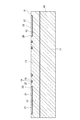
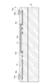
- 支持部と、
前記支持部に対して揺動自在に連結された可動部と、
前記可動部に埋め込まれるように設けられたコイルと、
前記コイルに磁界を作用させる磁界発生部と、
前記可動部の一の表面上に設けられた絶縁層と、
前記絶縁層上に設けられ、回折格子パターンが形成された樹脂層と、
前記回折格子パターンに沿うように前記樹脂層上に設けられた金属製の反射層と、を備え、
前記コイルは、前記可動部の前記表面に形成された溝内に配置されており、
前記コイルの幅は、前記コイルの厚さよりも大きい、可動回折格子。 - 前記回折格子パターンは、前記可動部の前記表面に垂直な方向から見た場合に前記コイルと重なる領域に配置されている、請求項1に記載の可動回折格子。
- 前記回折格子パターンは、中赤外領域の波長の光を回折させるブレーズドグレーティングパターンである、請求項1又は2に記載の可動回折格子。
- 請求項1〜3のいずれか一項に記載の可動回折格子の製造方法であって、
前記支持部及び前記可動部に対応する部分を含む基板を用意し、前記可動部に埋め込むように前記コイルを形成する第1ステップと、
前記第1ステップの後に、前記可動部の前記表面上に前記絶縁層を形成する第2ステップと、
前記第2ステップの後に、前記絶縁層上に樹脂材料を配置する第3ステップと、
前記第3ステップの後に、前記回折格子パターンに対応する転写パターンを有するモールドを用いて前記樹脂材料に前記転写パターンを転写することにより、前記回折格子パターンが形成された前記樹脂層を形成する第4ステップと、
前記第4ステップの後に、前記回折格子パターンに沿うように前記樹脂層上に前記反射層を形成する第5ステップと、を備える可動回折格子の製造方法。 - 請求項1〜3のいずれか一項に記載の可動回折格子と、
量子カスケードレーザ素子と、を備え、
前記可動回折格子は、前記量子カスケードレーザ素子により発振された光を回折させると共に反射させることにより、前記光のうち特定波長の光を前記量子カスケードレーザ素子に帰還させる、外部共振器型レーザモジュール。
Priority Applications (2)
| Application Number | Priority Date | Filing Date | Title |
|---|---|---|---|
| JP2016171192A JP6694355B2 (ja) | 2016-09-01 | 2016-09-01 | 可動回折格子及びその製造方法、並びに外部共振器型レーザモジュール |
| US15/687,637 US10361538B2 (en) | 2016-09-01 | 2017-08-28 | Movable diffraction grating, method of manufacturing the same, and external resonator type laser module |
Applications Claiming Priority (1)
| Application Number | Priority Date | Filing Date | Title |
|---|---|---|---|
| JP2016171192A JP6694355B2 (ja) | 2016-09-01 | 2016-09-01 | 可動回折格子及びその製造方法、並びに外部共振器型レーザモジュール |
Publications (2)
| Publication Number | Publication Date |
|---|---|
| JP2018036565A JP2018036565A (ja) | 2018-03-08 |
| JP6694355B2 true JP6694355B2 (ja) | 2020-05-13 |
Family
ID=61243715
Family Applications (1)
| Application Number | Title | Priority Date | Filing Date |
|---|---|---|---|
| JP2016171192A Active JP6694355B2 (ja) | 2016-09-01 | 2016-09-01 | 可動回折格子及びその製造方法、並びに外部共振器型レーザモジュール |
Country Status (2)
| Country | Link |
|---|---|
| US (1) | US10361538B2 (ja) |
| JP (1) | JP6694355B2 (ja) |
Families Citing this family (6)
| Publication number | Priority date | Publication date | Assignee | Title |
|---|---|---|---|---|
| KR102622543B1 (ko) * | 2018-09-19 | 2024-01-09 | 주식회사 위츠 | 코일 조립체 |
| JP7558081B2 (ja) * | 2021-02-24 | 2024-09-30 | 浜松ホトニクス株式会社 | 外部共振型レーザモジュール |
| JP7590889B2 (ja) * | 2021-02-24 | 2024-11-27 | 浜松ホトニクス株式会社 | 外部共振型レーザモジュール、及び外部共振型レーザモジュールの製造方法 |
| US12525768B2 (en) | 2021-02-24 | 2026-01-13 | Hamamatsu Photonics K.K. | External resonance-type laser module |
| JP7579174B2 (ja) * | 2021-02-24 | 2024-11-07 | 浜松ホトニクス株式会社 | 外部共振型レーザモジュール |
| JP7765925B2 (ja) * | 2021-09-21 | 2025-11-07 | 浜松ホトニクス株式会社 | 外部共振型レーザモジュール、及び外部共振型レーザモジュールの製造方法 |
Family Cites Families (16)
| Publication number | Priority date | Publication date | Assignee | Title |
|---|---|---|---|---|
| US6502757B1 (en) * | 1999-09-17 | 2003-01-07 | Dai Nippon Printing Co., Ltd. | Information recorded medium, device for reading the information, information recorded medium transfer foil, and method for producing information recorded medium |
| US6803843B2 (en) * | 2001-02-22 | 2004-10-12 | Canon Kabushiki Kaisha | Movable-body apparatus, optical deflector, and method of fabricating the same |
| JP2002250891A (ja) * | 2001-02-22 | 2002-09-06 | Canon Inc | 揺動体装置、光偏向器、及び光偏向器を用いた光学機器 |
| JP4144840B2 (ja) * | 2001-02-22 | 2008-09-03 | キヤノン株式会社 | 揺動体装置、光偏向器、及び光偏向器を用いた光学機器 |
| US6924915B2 (en) * | 2002-08-26 | 2005-08-02 | Canon Kabushiki Kaisha | Oscillation device, optical deflector using the oscillation device, and image display device and image forming apparatus using the optical deflector, and method of manufacturing the oscillation device |
| WO2004023464A1 (ja) * | 2002-09-06 | 2004-03-18 | Matsushita Electric Industrial Co., Ltd. | 光学ヘッド |
| JP2009036637A (ja) * | 2007-08-01 | 2009-02-19 | Sony Corp | 変位測定装置 |
| JP5351729B2 (ja) | 2009-12-03 | 2013-11-27 | パナソニック株式会社 | Mems光スキャナ |
| US8579443B2 (en) * | 2010-06-30 | 2013-11-12 | Microvision, Inc. | Scanned beam display having a redirected exit cone using a diffraction grating |
| JP5775325B2 (ja) * | 2011-02-25 | 2015-09-09 | 浜松ホトニクス株式会社 | 波長可変光源 |
| EP2689283A1 (en) * | 2011-03-25 | 2014-01-29 | Lemoptix SA | A reflective device |
| EP2506014B1 (en) * | 2011-03-30 | 2014-08-06 | Kabushiki Kaisha Toshiba | Measuring system using optical waveguide, measuring device, measuring method, optical waveguide type sensor chip, and magnetic fine particle |
| US10103613B2 (en) * | 2013-01-11 | 2018-10-16 | Intel Corporation | Mirror driving device |
| JP2015219153A (ja) * | 2014-05-19 | 2015-12-07 | パナソニックIpマネジメント株式会社 | スペクトルセンサ |
| JP6520209B2 (ja) * | 2015-02-27 | 2019-05-29 | セイコーエプソン株式会社 | 画像表示装置 |
| WO2016157419A1 (ja) * | 2015-03-31 | 2016-10-06 | パイオニア株式会社 | 光スキャナ |
-
2016
- 2016-09-01 JP JP2016171192A patent/JP6694355B2/ja active Active
-
2017
- 2017-08-28 US US15/687,637 patent/US10361538B2/en active Active
Also Published As
| Publication number | Publication date |
|---|---|
| US10361538B2 (en) | 2019-07-23 |
| JP2018036565A (ja) | 2018-03-08 |
| US20180062350A1 (en) | 2018-03-01 |
Similar Documents
| Publication | Publication Date | Title |
|---|---|---|
| JP6694355B2 (ja) | 可動回折格子及びその製造方法、並びに外部共振器型レーザモジュール | |
| US8559127B2 (en) | Integrated heat assisted magnetic recording head with extended cavity vertical cavity surface emitting laser diode | |
| JP5739224B2 (ja) | 光学部品の製造方法及び光学部品 | |
| CN101970995B (zh) | 分光器的制造方法 | |
| US11573296B2 (en) | Optical module and distance measurement device | |
| EP2626731B1 (en) | An optical coupling arrangement | |
| JP5715481B2 (ja) | 光モジュール及びその製造方法 | |
| JP2013243329A (ja) | 面発光レーザ素子及び原子発振器 | |
| KR20140082855A (ko) | 빛 파면의 제어 | |
| US11067728B2 (en) | Movable diffraction grating, external-resonator laser module, and manufacturing method for movable diffraction grating | |
| JP4950513B2 (ja) | 赤外線デバイス集積装置の製造方法 | |
| JP5707107B2 (ja) | 分光センサ | |
| CN111542933B (zh) | 发射辐射的半导体元件和制造发射辐射的半导体元件的方法 | |
| JP5515722B2 (ja) | 面発光型半導体レーザ、面発光型半導体レーザ装置、光伝送装置および情報処理装置 | |
| JP5929057B2 (ja) | 面発光型半導体レーザ、面発光型半導体レーザ装置、光伝送装置および情報処理装置 | |
| WO2019099945A1 (en) | Microsystems and semiconductor hybrid coherent light sources | |
| JP4112888B2 (ja) | 立体構造を持った微小光学系の製造方法とこれを実施した微小光学システム | |
| JP2006324409A (ja) | 半導体レーザ装置およびそれを備えた光ピックアップ装置 | |
| JP2008182245A (ja) | 有機半導体レーザー及びその製造方法 | |
| JP2009043367A (ja) | 光ヘッド装置 | |
| JP7758599B2 (ja) | 外部共振型レーザモジュール | |
| JP4914616B2 (ja) | 光学的情報読取装置用光走査モジュール及びその走査ミラー作成方法 | |
| JP2010239096A (ja) | 面発光素子およびその製造方法 | |
| CN101331656A (zh) | 用于微器件包装的载体基板 | |
| JPH10294527A (ja) | モノリシック受発光素子およびその製造方法およびそれを用いた光ピックアップ |
Legal Events
| Date | Code | Title | Description |
|---|---|---|---|
| A621 | Written request for application examination |
Free format text: JAPANESE INTERMEDIATE CODE: A621 Effective date: 20190426 |
|
| A977 | Report on retrieval |
Free format text: JAPANESE INTERMEDIATE CODE: A971007 Effective date: 20200212 |
|
| A131 | Notification of reasons for refusal |
Free format text: JAPANESE INTERMEDIATE CODE: A131 Effective date: 20200218 |
|
| A521 | Request for written amendment filed |
Free format text: JAPANESE INTERMEDIATE CODE: A523 Effective date: 20200401 |
|
| TRDD | Decision of grant or rejection written | ||
| A01 | Written decision to grant a patent or to grant a registration (utility model) |
Free format text: JAPANESE INTERMEDIATE CODE: A01 Effective date: 20200414 |
|
| A61 | First payment of annual fees (during grant procedure) |
Free format text: JAPANESE INTERMEDIATE CODE: A61 Effective date: 20200417 |
|
| R150 | Certificate of patent or registration of utility model |
Ref document number: 6694355 Country of ref document: JP Free format text: JAPANESE INTERMEDIATE CODE: R150 |
|
| R250 | Receipt of annual fees |
Free format text: JAPANESE INTERMEDIATE CODE: R250 |
|
| R250 | Receipt of annual fees |
Free format text: JAPANESE INTERMEDIATE CODE: R250 |
|
| R250 | Receipt of annual fees |
Free format text: JAPANESE INTERMEDIATE CODE: R250 |