JP6700550B2 - レギュレータ - Google Patents
レギュレータ Download PDFInfo
- Publication number
- JP6700550B2 JP6700550B2 JP2016002342A JP2016002342A JP6700550B2 JP 6700550 B2 JP6700550 B2 JP 6700550B2 JP 2016002342 A JP2016002342 A JP 2016002342A JP 2016002342 A JP2016002342 A JP 2016002342A JP 6700550 B2 JP6700550 B2 JP 6700550B2
- Authority
- JP
- Japan
- Prior art keywords
- output
- mos transistor
- terminal
- voltage
- transistor
- Prior art date
- Legal status (The legal status is an assumption and is not a legal conclusion. Google has not performed a legal analysis and makes no representation as to the accuracy of the status listed.)
- Expired - Fee Related
Links
Images



Classifications
-
- G—PHYSICS
- G05—CONTROLLING; REGULATING
- G05F—SYSTEMS FOR REGULATING ELECTRIC OR MAGNETIC VARIABLES
- G05F1/00—Automatic systems in which deviations of an electric quantity from one or more predetermined values are detected at the output of the system and fed back to a device within the system to restore the detected quantity to its predetermined value or values, i.e. retroactive systems
- G05F1/10—Regulating voltage or current
- G05F1/46—Regulating voltage or current wherein the variable actually regulated by the final control device is DC
- G05F1/56—Regulating voltage or current wherein the variable actually regulated by the final control device is DC using semiconductor devices in series with the load as final control devices
- G05F1/565—Regulating voltage or current wherein the variable actually regulated by the final control device is DC using semiconductor devices in series with the load as final control devices sensing a condition of the system or its load in addition to means responsive to deviations in the output of the system, e.g. current, voltage, power factor
- G05F1/569—Regulating voltage or current wherein the variable actually regulated by the final control device is DC using semiconductor devices in series with the load as final control devices sensing a condition of the system or its load in addition to means responsive to deviations in the output of the system, e.g. current, voltage, power factor for protection
- G05F1/573—Regulating voltage or current wherein the variable actually regulated by the final control device is DC using semiconductor devices in series with the load as final control devices sensing a condition of the system or its load in addition to means responsive to deviations in the output of the system, e.g. current, voltage, power factor for protection with overcurrent detector
-
- G—PHYSICS
- G05—CONTROLLING; REGULATING
- G05F—SYSTEMS FOR REGULATING ELECTRIC OR MAGNETIC VARIABLES
- G05F1/00—Automatic systems in which deviations of an electric quantity from one or more predetermined values are detected at the output of the system and fed back to a device within the system to restore the detected quantity to its predetermined value or values, i.e. retroactive systems
- G05F1/10—Regulating voltage or current
- G05F1/46—Regulating voltage or current wherein the variable actually regulated by the final control device is DC
- G05F1/56—Regulating voltage or current wherein the variable actually regulated by the final control device is DC using semiconductor devices in series with the load as final control devices
Landscapes
- Engineering & Computer Science (AREA)
- Physics & Mathematics (AREA)
- Electromagnetism (AREA)
- General Physics & Mathematics (AREA)
- Radar, Positioning & Navigation (AREA)
- Automation & Control Theory (AREA)
- Continuous-Control Power Sources That Use Transistors (AREA)
- Amplifiers (AREA)
Description
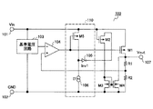
図1は、第1の実施形態に係るレギュレータの構成図である。
第2の実施形態では、図1に示した第1の実施形態に係るレギュレータ100の信号処理回路110の別の一例について説明する。
第3の実施形態では、図1に示した第1の実施形態に係るレギュレータ100の別の一例について説明する。
第4の実施形態では、図2に示した第2の実施形態に係るレギュレータ100の別の一例について説明する。
101 第1の端子
102 第2の端子
103 基準電圧回路
104 誤差増幅回路
105 インバータ
106 電流源
107 出力端子
110、210 信号処理回路
211 コンパレータ
212 基準電圧
M1 出力トランジスタ
M2 第1のMOSトランジスタ
M3 第2のMOSトランジスタ
M4 第3のMOSトランジスタ
M5 第4のMOSトランジスタ
Claims (6)
- レギュレータの出力電圧が出力される出力端子と、
前記レギュレータの第1の端子と第2の端子との間に接続された基準電圧回路と、
2つの入力を有し、一方の入力に前記基準電圧回路の出力が接続された誤差増幅回路と、
前記第1の端子にソースが接続され、前記誤差増幅回路の出力によって制御され、前記出力電圧を出力する第1導電型の出力トランジスタと、
前記第1の端子と前記第2の端子との間に前記出力トランジスタと直列に接続され、前記出力トランジスタの前記出力電圧を分圧し、分圧した分圧電圧が前記誤差増幅回路の他方の入力に接続された分圧抵抗と、
前記第1の端子にゲートが接続された第1導電型の第1のMOSトランジスタと、
前記第1のMOSトランジスタのドレインと前記第2の端子との間に接続され、ソースが前記第2の端子に接続され、ゲートとドレインが接続された第2導電型の第2のMOSトランジスタと、
ドレインが前記出力トランジスタのドレインと接続され、ゲートが前記第2のMOSトランジスタのゲートに接続され、ソースが前記第2の端子に接続された第2導電型の第3のMOSトランジスタと、
前記誤差増幅回路の出力に応じて、前記第1の端子の電圧と同等の電圧と、前記第2の端子の電圧と同等の電圧との、いずれかの電圧を出力する信号処理回路と、
を有し、
前記誤差増幅回路の出力が、前記信号処理回路の出力を介して前記第1のMOSトランジスタのソースに接続されていることを特徴とするレギュレータ。 - 前記信号処理回路は、
ゲートが前記誤差増幅回路の出力に接続され、ソースが前記第1の端子に接続された第1導電型の第4のMOSトランジスタと、
前記第4のMOSトランジスタのドレインと前記第2の端子との間に接続された電流源と、
入力と出力を有するインバータと、
を有し、
前記第4のMOSトランジスタのドレインが、前記インバータの前記入力に接続され、
前記インバータの前記出力が、前記第1のMOSトランジスタのソースに接続されていることを特徴とする請求項1に記載のレギュレータ。 - 前記信号処理回路は、
ゲートが前記誤差増幅回路の出力に接続され、ソースが前記第1の端子に接続された第1導電型の第4のMOSトランジスタと、
前記第4のMOSトランジスタのドレインと前記第2の端子との間に接続された電流源と、
二つの入力を有するコンパレータと、
を有し、
前記第4のMOSトランジスタのドレインが、前記コンパレータの一方の入力に接続され、前記コンパレータの他方の入力に基準電圧が接続され、
前記コンパレータの出力が、前記第1のMOSトランジスタのソースに接続されていることを特徴とする請求項1に記載のレギュレータ。 - レギュレータの出力電圧が出力される出力端子と、
前記レギュレータの第1の端子と第2の端子との間に接続された基準電圧回路と、
2つの入力を有し、一方の入力に前記基準電圧回路の出力が接続された誤差増幅回路と、
前記第1の端子にソースが接続され、前記誤差増幅回路の出力によって制御され、前記出力電圧を出力する第1導電型の出力トランジスタと、
前記第1の端子と前記第2の端子との間に前記出力トランジスタと直列に接続され、前記出力トランジスタの前記出力電圧を分圧し、分圧した分圧電圧が前記誤差増幅回路の他方の入力に接続された分圧抵抗と、
ゲートとソースが接続された第1導電型の第1のMOSトランジスタと、
前記第1のMOSトランジスタのドレインと前記第2の端子との間に接続され、ソースが前記第2の端子に接続され、ゲートとドレインが接続された第2導電型の第2のMOSトランジスタと、
ドレインが前記出力トランジスタのドレインと接続され、ゲートが前記第2のMOSトランジスタのゲートに接続され、ソースが前記第2の端子に接続された第2導電型の第3のMOSトランジスタと、
前記誤差増幅回路の出力に応じて、前記第1の端子の電圧と同等の電圧と、前記第2の端子の電圧と同等の電圧との、いずれかの電圧を出力する信号処理回路と、
を有し、
前記誤差増幅回路の出力が、前記信号処理回路の出力を介して前記第1のMOSトランジスタのゲートとソースに接続されていることを特徴とするレギュレータ。 - 前記信号処理回路は、
ゲートが前記誤差増幅回路の出力に接続され、ソースが前記第1の端子に接続された第1導電型の第4のMOSトランジスタと、
前記第4のMOSトランジスタのドレインと前記第2の端子との間に接続された電流源と、
入力と出力を有するインバータと、
を有し、
前記第4のMOSトランジスタのドレインが、前記インバータの前記入力に接続され、
前記インバータの前記出力が、前記第1のMOSトランジスタのゲートとソースに接続されていることを特徴とする請求項4に記載のレギュレータ。 - 前記信号処理回路は、
ゲートが前記誤差増幅回路の出力に接続され、ソースが前記第1の端子に接続された第1導電型の第4のMOSトランジスタと、
前記第4のMOSトランジスタのドレインと前記第2の端子との間に接続された電流源と、
二つの入力を有するコンパレータと、
を有し、
前記第4のMOSトランジスタのドレインが、前記コンパレータの一方の入力に接続され、前記コンパレータの他方の入力に基準電圧が接続され、
前記コンパレータの出力が、前記第1のMOSトランジスタのゲートとソースに接続されていることを特徴とする請求項4に記載のレギュレータ。
Priority Applications (3)
| Application Number | Priority Date | Filing Date | Title |
|---|---|---|---|
| JP2016002342A JP6700550B2 (ja) | 2016-01-08 | 2016-01-08 | レギュレータ |
| US15/352,791 US9785163B2 (en) | 2016-01-08 | 2016-11-16 | Regulator |
| CN201611170438.XA CN106959718A (zh) | 2016-01-08 | 2016-12-16 | 调节器 |
Applications Claiming Priority (1)
| Application Number | Priority Date | Filing Date | Title |
|---|---|---|---|
| JP2016002342A JP6700550B2 (ja) | 2016-01-08 | 2016-01-08 | レギュレータ |
Publications (2)
| Publication Number | Publication Date |
|---|---|
| JP2017123091A JP2017123091A (ja) | 2017-07-13 |
| JP6700550B2 true JP6700550B2 (ja) | 2020-05-27 |
Family
ID=59276353
Family Applications (1)
| Application Number | Title | Priority Date | Filing Date |
|---|---|---|---|
| JP2016002342A Expired - Fee Related JP6700550B2 (ja) | 2016-01-08 | 2016-01-08 | レギュレータ |
Country Status (3)
| Country | Link |
|---|---|
| US (1) | US9785163B2 (ja) |
| JP (1) | JP6700550B2 (ja) |
| CN (1) | CN106959718A (ja) |
Families Citing this family (4)
| Publication number | Priority date | Publication date | Assignee | Title |
|---|---|---|---|---|
| CN107167164B (zh) * | 2016-03-08 | 2020-11-06 | 艾普凌科有限公司 | 磁传感器和磁传感器装置 |
| CN106788356B (zh) * | 2016-12-13 | 2019-04-26 | 电子科技大学 | 一种具有实时频率补偿功能的线性稳压器 |
| JP6986999B2 (ja) * | 2018-03-15 | 2021-12-22 | エイブリック株式会社 | ボルテージレギュレータ |
| CN113672024B (zh) * | 2021-07-21 | 2022-11-01 | 北京时代民芯科技有限公司 | 一种应用于低功耗ldo的漏电流补偿电路及方法 |
Family Cites Families (7)
| Publication number | Priority date | Publication date | Assignee | Title |
|---|---|---|---|---|
| JP2953887B2 (ja) | 1992-10-24 | 1999-09-27 | 日本電気アイシーマイコンシステム株式会社 | ボルテージレギュレータ |
| JP3452459B2 (ja) * | 1997-04-25 | 2003-09-29 | セイコーインスツルメンツ株式会社 | ボルテージレギュレータ |
| JP2000194431A (ja) * | 1998-12-24 | 2000-07-14 | Rohm Co Ltd | 安定化電源回路 |
| JP4855841B2 (ja) * | 2006-06-14 | 2012-01-18 | 株式会社リコー | 定電圧回路及びその出力電圧制御方法 |
| JP6205142B2 (ja) * | 2013-03-08 | 2017-09-27 | エスアイアイ・セミコンダクタ株式会社 | 定電圧回路 |
| JP6211889B2 (ja) | 2013-10-22 | 2017-10-11 | エスアイアイ・セミコンダクタ株式会社 | ボルテージレギュレータ |
| US9665111B2 (en) * | 2014-01-29 | 2017-05-30 | Semiconductor Components Industries, Llc | Low dropout voltage regulator and method |
-
2016
- 2016-01-08 JP JP2016002342A patent/JP6700550B2/ja not_active Expired - Fee Related
- 2016-11-16 US US15/352,791 patent/US9785163B2/en not_active Expired - Fee Related
- 2016-12-16 CN CN201611170438.XA patent/CN106959718A/zh active Pending
Also Published As
| Publication number | Publication date |
|---|---|
| JP2017123091A (ja) | 2017-07-13 |
| US20170199535A1 (en) | 2017-07-13 |
| CN106959718A (zh) | 2017-07-18 |
| US9785163B2 (en) | 2017-10-10 |
Similar Documents
| Publication | Publication Date | Title |
|---|---|---|
| JP5516320B2 (ja) | レギュレータ用半導体集積回路 | |
| US8680828B2 (en) | Voltage regulator | |
| US8665020B2 (en) | Differential amplifier circuit that can change current flowing through a constant-current source according to load variation, and series regulator including the same | |
| JP5008472B2 (ja) | ボルテージレギュレータ | |
| US9298200B2 (en) | Constant voltage circuit with drooping and foldback overcurrent protection | |
| US9372489B2 (en) | Voltage regulator having a temperature sensitive leakage current sink circuit | |
| JP5279544B2 (ja) | ボルテージレギュレータ | |
| US9348350B2 (en) | Voltage regulator | |
| US9411345B2 (en) | Voltage regulator | |
| US9831757B2 (en) | Voltage regulator | |
| JP6513943B2 (ja) | ボルテージレギュレータ | |
| US20080265856A1 (en) | Constant-voltage power circuit | |
| JP6700550B2 (ja) | レギュレータ | |
| JP2008217203A (ja) | レギュレータ回路 | |
| US10444777B2 (en) | Reverse-current-prevention circuit and power supply circuit | |
| JP2013239153A (ja) | 可変電源の温度補償電源電圧の出力回路及びその方法 | |
| JP2018173868A (ja) | 過電流保護回路及びボルテージレギュレータ | |
| JP5434170B2 (ja) | 過電流保護装置 | |
| TWI672572B (zh) | 電壓調節器 | |
| JP2016015076A (ja) | レギュレータ回路 | |
| US10551860B2 (en) | Regulator for reducing power consumption | |
| JP2014164702A (ja) | ボルテージレギュレータ | |
| US9891642B2 (en) | Current source and current supply system with hysteresis | |
| US9654074B2 (en) | Variable gain amplifier circuit, controller of main amplifier and associated control method |
Legal Events
| Date | Code | Title | Description |
|---|---|---|---|
| A521 | Request for written amendment filed |
Free format text: JAPANESE INTERMEDIATE CODE: A523 Effective date: 20161121 |
|
| A621 | Written request for application examination |
Free format text: JAPANESE INTERMEDIATE CODE: A621 Effective date: 20181210 |
|
| A977 | Report on retrieval |
Free format text: JAPANESE INTERMEDIATE CODE: A971007 Effective date: 20191003 |
|
| A131 | Notification of reasons for refusal |
Free format text: JAPANESE INTERMEDIATE CODE: A131 Effective date: 20191008 |
|
| A521 | Request for written amendment filed |
Free format text: JAPANESE INTERMEDIATE CODE: A523 Effective date: 20191025 |
|
| A131 | Notification of reasons for refusal |
Free format text: JAPANESE INTERMEDIATE CODE: A131 Effective date: 20200204 |
|
| A521 | Request for written amendment filed |
Free format text: JAPANESE INTERMEDIATE CODE: A523 Effective date: 20200316 |
|
| TRDD | Decision of grant or rejection written | ||
| A01 | Written decision to grant a patent or to grant a registration (utility model) |
Free format text: JAPANESE INTERMEDIATE CODE: A01 Effective date: 20200331 |
|
| A61 | First payment of annual fees (during grant procedure) |
Free format text: JAPANESE INTERMEDIATE CODE: A61 Effective date: 20200413 |
|
| R150 | Certificate of patent or registration of utility model |
Ref document number: 6700550 Country of ref document: JP Free format text: JAPANESE INTERMEDIATE CODE: R150 |
|
| LAPS | Cancellation because of no payment of annual fees |