JP6711005B2 - 画素ユニット、及び撮像素子 - Google Patents
画素ユニット、及び撮像素子 Download PDFInfo
- Publication number
- JP6711005B2 JP6711005B2 JP2016032187A JP2016032187A JP6711005B2 JP 6711005 B2 JP6711005 B2 JP 6711005B2 JP 2016032187 A JP2016032187 A JP 2016032187A JP 2016032187 A JP2016032187 A JP 2016032187A JP 6711005 B2 JP6711005 B2 JP 6711005B2
- Authority
- JP
- Japan
- Prior art keywords
- region
- transistor
- pixel unit
- pixel
- diffusion region
- Prior art date
- Legal status (The legal status is an assumption and is not a legal conclusion. Google has not performed a legal analysis and makes no representation as to the accuracy of the status listed.)
- Active
Links
Images






Classifications
-
- H—ELECTRICITY
- H04—ELECTRIC COMMUNICATION TECHNIQUE
- H04N—PICTORIAL COMMUNICATION, e.g. TELEVISION
- H04N25/00—Circuitry of solid-state image sensors [SSIS]; Control thereof
- H04N25/70—SSIS architectures; Circuits associated therewith
- H04N25/76—Addressed sensors, e.g. MOS or CMOS sensors
-
- H—ELECTRICITY
- H04—ELECTRIC COMMUNICATION TECHNIQUE
- H04N—PICTORIAL COMMUNICATION, e.g. TELEVISION
- H04N25/00—Circuitry of solid-state image sensors [SSIS]; Control thereof
- H04N25/70—SSIS architectures; Circuits associated therewith
- H04N25/76—Addressed sensors, e.g. MOS or CMOS sensors
- H04N25/78—Readout circuits for addressed sensors, e.g. output amplifiers or A/D converters
-
- H—ELECTRICITY
- H10—SEMICONDUCTOR DEVICES; ELECTRIC SOLID-STATE DEVICES NOT OTHERWISE PROVIDED FOR
- H10F—INORGANIC SEMICONDUCTOR DEVICES SENSITIVE TO INFRARED RADIATION, LIGHT, ELECTROMAGNETIC RADIATION OF SHORTER WAVELENGTH OR CORPUSCULAR RADIATION
- H10F39/00—Integrated devices, or assemblies of multiple devices, comprising at least one element covered by group H10F30/00, e.g. radiation detectors comprising photodiode arrays
- H10F39/10—Integrated devices
- H10F39/12—Image sensors
- H10F39/18—Complementary metal-oxide-semiconductor [CMOS] image sensors; Photodiode array image sensors
-
- H—ELECTRICITY
- H10—SEMICONDUCTOR DEVICES; ELECTRIC SOLID-STATE DEVICES NOT OTHERWISE PROVIDED FOR
- H10F—INORGANIC SEMICONDUCTOR DEVICES SENSITIVE TO INFRARED RADIATION, LIGHT, ELECTROMAGNETIC RADIATION OF SHORTER WAVELENGTH OR CORPUSCULAR RADIATION
- H10F39/00—Integrated devices, or assemblies of multiple devices, comprising at least one element covered by group H10F30/00, e.g. radiation detectors comprising photodiode arrays
- H10F39/80—Constructional details of image sensors
- H10F39/802—Geometry or disposition of elements in pixels, e.g. address-lines or gate electrodes
- H10F39/8023—Disposition of the elements in pixels, e.g. smaller elements in the centre of the imager compared to larger elements at the periphery
-
- H—ELECTRICITY
- H10—SEMICONDUCTOR DEVICES; ELECTRIC SOLID-STATE DEVICES NOT OTHERWISE PROVIDED FOR
- H10F—INORGANIC SEMICONDUCTOR DEVICES SENSITIVE TO INFRARED RADIATION, LIGHT, ELECTROMAGNETIC RADIATION OF SHORTER WAVELENGTH OR CORPUSCULAR RADIATION
- H10F39/00—Integrated devices, or assemblies of multiple devices, comprising at least one element covered by group H10F30/00, e.g. radiation detectors comprising photodiode arrays
- H10F39/80—Constructional details of image sensors
- H10F39/803—Pixels having integrated switching, control, storage or amplification elements
- H10F39/8037—Pixels having integrated switching, control, storage or amplification elements the integrated elements comprising a transistor
Landscapes
- Engineering & Computer Science (AREA)
- Multimedia (AREA)
- Signal Processing (AREA)
- Solid State Image Pick-Up Elements (AREA)
- Transforming Light Signals Into Electric Signals (AREA)
Description
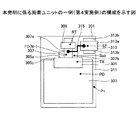
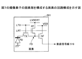
3,103,203,303,403 フォトダイオード
5,105,205,305,405 転送トランジスタ
5b 延長部
7,107,207,307,407 フローティングディフュージョン領域
7a,107a,207a,307a,407a 高濃度領域
7b,107b,207b,307b,407b 低濃度領域(半導体基板)
9,109,209,309,409 リセットトランジスタ
11,111,211,311,411 分離領域
313,413 増幅トランジスタ
317,417 画素群
319,419,519 垂直信号線
523,623 固体撮像素子
631 カメラシステム
Claims (9)
- 光電変換素子と、
前記光電変換素子に接続して前記光電変換素子で光電変換した電荷を転送する第1のトランジスタと、
前記第1のトランジスタにより転送された電荷をリセットする第2のトランジスタと、
前記第1のトランジスタと前記第2のトランジスタの間に設けられて、拡散した不純物を含みかつ前記第1のトランジスタから転送された電荷を蓄積する拡散領域とを備える画素ユニットであって、
前記拡散領域は、
前記第1のトランジスタのゲート及び前記第2のトランジスタのゲートに接続する第1の領域と、
前記第1の領域に隣接して、前記第1のトランジスタのゲートに接続し且つ前記第2のトランジスタのゲートに接続しない第2の領域とを含み、
前記第2の領域の不純物濃度が、前記第1の領域の不純物濃度よりも低いことを特徴とする画素ユニット。 - 前記拡散領域の周辺には、素子分離領域が設けられており、
前記第2の領域は、前記第1の領域と前記素子分離領域とを隔てるように、前記第1の領域と前記素子分離領域との間に存在する請求項1に記載の画素ユニット。 - 前記第2の領域は、平面視において、前記第1の領域を挟むように前記第1の領域に隣接する請求項1または2に記載の画素ユニット。
- 前記第1のトランジスタ、前記第2のトランジスタ、及び前記第1の領域が、半導体基板の上に形成されており、
前記第2の領域が前記半導体基板の一部で構成されている請求項1乃至3のいずれかに記載の画素ユニット。 - 前記拡散領域に接続して前記拡散領域で変換した信号電圧を増幅する第3のトランジスタをさらに備える請求項1乃至3のいずれか1項に記載の画素ユニット。
- 前記拡散領域の一部が前記第1のトランジスタの一部で構成されている請求項1乃至5のいずれか1項に記載の画素ユニット。
- 前記第1のトランジスタのゲートは、前記光電変換素子から前記拡散領域側にせり出した位置で前記第1の領域に接続する請求項1乃至5のいずれか1項に記載の画素ユニット。
- 請求項1乃至7のいずれか1項に記載の画素ユニットが複数配置された撮像素子であって、
前記画素ユニットのうち、一部の画素ユニットが第1の方向に並んで配置された画素ユニット列を構成し、
前記画素ユニット列がさらに第1の方向と直交する第2の方向に複数並んで配置された撮像素子。 - 前記画素ユニット列を構成する前記一部の画素ユニットは、前記画素ユニットの電気信号を読み出す1つの信号線に接続されている請求項8に記載の撮像素子。
Priority Applications (2)
| Application Number | Priority Date | Filing Date | Title |
|---|---|---|---|
| JP2016032187A JP6711005B2 (ja) | 2016-02-23 | 2016-02-23 | 画素ユニット、及び撮像素子 |
| US15/426,152 US9924120B2 (en) | 2016-02-23 | 2017-02-07 | Pixel unit and image sensor |
Applications Claiming Priority (1)
| Application Number | Priority Date | Filing Date | Title |
|---|---|---|---|
| JP2016032187A JP6711005B2 (ja) | 2016-02-23 | 2016-02-23 | 画素ユニット、及び撮像素子 |
Publications (2)
| Publication Number | Publication Date |
|---|---|
| JP2017152481A JP2017152481A (ja) | 2017-08-31 |
| JP6711005B2 true JP6711005B2 (ja) | 2020-06-17 |
Family
ID=59629617
Family Applications (1)
| Application Number | Title | Priority Date | Filing Date |
|---|---|---|---|
| JP2016032187A Active JP6711005B2 (ja) | 2016-02-23 | 2016-02-23 | 画素ユニット、及び撮像素子 |
Country Status (2)
| Country | Link |
|---|---|
| US (1) | US9924120B2 (ja) |
| JP (1) | JP6711005B2 (ja) |
Families Citing this family (4)
| Publication number | Priority date | Publication date | Assignee | Title |
|---|---|---|---|---|
| JP6769349B2 (ja) | 2017-03-03 | 2020-10-14 | 株式会社リコー | 固体撮像素子及び撮像装置 |
| JP6969224B2 (ja) | 2017-08-24 | 2021-11-24 | 株式会社リコー | 固体撮像素子及び撮像装置 |
| JP7013973B2 (ja) | 2018-03-19 | 2022-02-01 | 株式会社リコー | 固体撮像素子及び撮像装置 |
| KR102651393B1 (ko) * | 2019-04-05 | 2024-03-27 | 에스케이하이닉스 주식회사 | 쉴딩 배선을 갖는 이미지 센서 |
Family Cites Families (24)
| Publication number | Priority date | Publication date | Assignee | Title |
|---|---|---|---|---|
| JP3792628B2 (ja) * | 2002-09-02 | 2006-07-05 | 富士通株式会社 | 固体撮像装置及び画像読み出し方法 |
| KR100508086B1 (ko) * | 2002-09-11 | 2005-08-17 | 삼성전자주식회사 | 씨모스 이미지 센서 및 그 제조방법 |
| JP3794637B2 (ja) * | 2003-03-07 | 2006-07-05 | 松下電器産業株式会社 | 固体撮像装置 |
| JP5140235B2 (ja) * | 2003-03-19 | 2013-02-06 | 富士通セミコンダクター株式会社 | 半導体装置 |
| US7064406B2 (en) * | 2003-09-03 | 2006-06-20 | Micron Technology, Inc. | Supression of dark current in a photosensor for imaging |
| JP4581792B2 (ja) * | 2004-07-05 | 2010-11-17 | コニカミノルタホールディングス株式会社 | 固体撮像装置及びこれを備えたカメラ |
| KR100630704B1 (ko) * | 2004-10-20 | 2006-10-02 | 삼성전자주식회사 | 비평면 구조의 트랜지스터를 구비한 cmos 이미지 센서및 그 제조 방법 |
| US7663167B2 (en) * | 2004-12-23 | 2010-02-16 | Aptina Imaging Corp. | Split transfer gate for dark current suppression in an imager pixel |
| JP4459064B2 (ja) * | 2005-01-14 | 2010-04-28 | キヤノン株式会社 | 固体撮像装置、その制御方法及びカメラ |
| JP2007053217A (ja) * | 2005-08-18 | 2007-03-01 | Renesas Technology Corp | 固体撮像素子 |
| US7521742B2 (en) * | 2006-06-05 | 2009-04-21 | Samsung Electronics Co., Ltd. | Complementary metal oxide semiconductor (CMOS) image sensor |
| US7916195B2 (en) * | 2006-10-13 | 2011-03-29 | Sony Corporation | Solid-state imaging device, imaging apparatus and camera |
| JP5292787B2 (ja) * | 2007-11-30 | 2013-09-18 | ソニー株式会社 | 固体撮像装置及びカメラ |
| JP5029624B2 (ja) * | 2009-01-15 | 2012-09-19 | ソニー株式会社 | 固体撮像装置及び電子機器 |
| JP2010200025A (ja) * | 2009-02-25 | 2010-09-09 | Panasonic Corp | 固体撮像装置 |
| TWI467751B (zh) * | 2011-12-12 | 2015-01-01 | Sony Corp | A solid-state imaging device, a driving method of a solid-state imaging device, and an electronic device |
| JP2013225774A (ja) * | 2012-04-20 | 2013-10-31 | Brookman Technology Inc | 固体撮像装置 |
| JP2015106908A (ja) | 2013-12-03 | 2015-06-08 | 株式会社リコー | カラム読出し回路および固体撮像装置 |
| JP6445799B2 (ja) * | 2014-07-08 | 2018-12-26 | キヤノン株式会社 | 光電変換装置 |
| CN106537897B (zh) * | 2014-07-09 | 2020-01-24 | 瑞萨电子株式会社 | 半导体器件 |
| KR102253003B1 (ko) * | 2014-07-11 | 2021-05-17 | 삼성전자주식회사 | 이미지 센서의 픽셀 어레이 및 이미지 센서 |
| US20160172397A1 (en) * | 2014-12-15 | 2016-06-16 | Dartmouth College | Solid State Image Sensor with Low Capacitance Floating Diffusion |
| JP2016139660A (ja) * | 2015-01-26 | 2016-08-04 | 株式会社東芝 | 固体撮像装置 |
| JP2015130533A (ja) | 2015-03-31 | 2015-07-16 | ソニー株式会社 | 固体撮像装置及びカメラ |
-
2016
- 2016-02-23 JP JP2016032187A patent/JP6711005B2/ja active Active
-
2017
- 2017-02-07 US US15/426,152 patent/US9924120B2/en active Active
Also Published As
| Publication number | Publication date |
|---|---|
| JP2017152481A (ja) | 2017-08-31 |
| US20170244919A1 (en) | 2017-08-24 |
| US9924120B2 (en) | 2018-03-20 |
Similar Documents
| Publication | Publication Date | Title |
|---|---|---|
| US8031250B2 (en) | Solid-state imaging device and method of driving the same | |
| KR100657863B1 (ko) | 핑거드 타입 소스 폴로워 트랜지스터를 이용한 상보성금속 산화막 반도체 액티브 픽셀 센서 | |
| JP5292787B2 (ja) | 固体撮像装置及びカメラ | |
| JP5531580B2 (ja) | 固体撮像装置、および、その製造方法、電子機器 | |
| JP5688540B2 (ja) | 固体撮像装置およびカメラ | |
| CN102316281B (zh) | 固态成像装置和成像系统 | |
| US20130140442A1 (en) | Amplifying circuit and manufacturing method, solid-state imaging element, and electronic device | |
| JP2010206172A (ja) | 撮像装置およびカメラ | |
| JP2008004692A (ja) | 固体撮像装置 | |
| JP6842240B2 (ja) | 画素ユニット、及び撮像素子 | |
| JP2013045878A (ja) | 固体撮像装置、固体撮像装置の製造方法、電子機器 | |
| JP6711005B2 (ja) | 画素ユニット、及び撮像素子 | |
| CN100429780C (zh) | 固体摄像装置 | |
| CN104600086A (zh) | 固体摄像装置以及固体摄像装置的制造方法 | |
| JP2015130533A (ja) | 固体撮像装置及びカメラ | |
| JP7115067B2 (ja) | 固体撮像素子及び撮像システム | |
| JP2008218756A (ja) | 光電変換装置及び撮像システム | |
| JP6897740B2 (ja) | 画素ユニット、及び撮像素子 | |
| JP2011142188A (ja) | 固体撮像素子 | |
| JP2019134418A (ja) | 固体撮像素子、その駆動回路および撮像装置 | |
| JP6536627B2 (ja) | 固体撮像装置及び電子機器 | |
| JP2007134639A (ja) | 光電変換装置及びそれを用いた撮像素子 | |
| JP4720402B2 (ja) | 固体撮像装置 | |
| JP5725232B2 (ja) | 固体撮像装置及びカメラ | |
| JP2004104116A (ja) | 撮像装置 |
Legal Events
| Date | Code | Title | Description |
|---|---|---|---|
| A621 | Written request for application examination |
Free format text: JAPANESE INTERMEDIATE CODE: A621 Effective date: 20190109 |
|
| A977 | Report on retrieval |
Free format text: JAPANESE INTERMEDIATE CODE: A971007 Effective date: 20191015 |
|
| A131 | Notification of reasons for refusal |
Free format text: JAPANESE INTERMEDIATE CODE: A131 Effective date: 20191126 |
|
| A521 | Request for written amendment filed |
Free format text: JAPANESE INTERMEDIATE CODE: A523 Effective date: 20200123 |
|
| TRDD | Decision of grant or rejection written | ||
| A01 | Written decision to grant a patent or to grant a registration (utility model) |
Free format text: JAPANESE INTERMEDIATE CODE: A01 Effective date: 20200428 |
|
| A61 | First payment of annual fees (during grant procedure) |
Free format text: JAPANESE INTERMEDIATE CODE: A61 Effective date: 20200511 |
|
| R151 | Written notification of patent or utility model registration |
Ref document number: 6711005 Country of ref document: JP Free format text: JAPANESE INTERMEDIATE CODE: R151 |