JP6711657B2 - タッチパネル - Google Patents
タッチパネル Download PDFInfo
- Publication number
- JP6711657B2 JP6711657B2 JP2016059490A JP2016059490A JP6711657B2 JP 6711657 B2 JP6711657 B2 JP 6711657B2 JP 2016059490 A JP2016059490 A JP 2016059490A JP 2016059490 A JP2016059490 A JP 2016059490A JP 6711657 B2 JP6711657 B2 JP 6711657B2
- Authority
- JP
- Japan
- Prior art keywords
- electrode
- layer
- substrate
- film
- liquid crystal
- Prior art date
- Legal status (The legal status is an assumption and is not a legal conclusion. Google has not performed a legal analysis and makes no representation as to the accuracy of the status listed.)
- Active
Links
Images





Classifications
-
- G—PHYSICS
- G02—OPTICS
- G02F—OPTICAL DEVICES OR ARRANGEMENTS FOR THE CONTROL OF LIGHT BY MODIFICATION OF THE OPTICAL PROPERTIES OF THE MEDIA OF THE ELEMENTS INVOLVED THEREIN; NON-LINEAR OPTICS; FREQUENCY-CHANGING OF LIGHT; OPTICAL LOGIC ELEMENTS; OPTICAL ANALOGUE/DIGITAL CONVERTERS
- G02F1/00—Devices or arrangements for the control of the intensity, colour, phase, polarisation or direction of light arriving from an independent light source, e.g. switching, gating or modulating; Non-linear optics
- G02F1/01—Devices or arrangements for the control of the intensity, colour, phase, polarisation or direction of light arriving from an independent light source, e.g. switching, gating or modulating; Non-linear optics for the control of the intensity, phase, polarisation or colour
- G02F1/13—Devices or arrangements for the control of the intensity, colour, phase, polarisation or direction of light arriving from an independent light source, e.g. switching, gating or modulating; Non-linear optics for the control of the intensity, phase, polarisation or colour based on liquid crystals, e.g. single liquid crystal display cells
- G02F1/133—Constructional arrangements; Operation of liquid crystal cells; Circuit arrangements
- G02F1/1333—Constructional arrangements; Manufacturing methods
- G02F1/13338—Input devices, e.g. touch panels
-
- G—PHYSICS
- G06—COMPUTING OR CALCULATING; COUNTING
- G06F—ELECTRIC DIGITAL DATA PROCESSING
- G06F3/00—Input arrangements for transferring data to be processed into a form capable of being handled by the computer; Output arrangements for transferring data from processing unit to output unit, e.g. interface arrangements
- G06F3/01—Input arrangements or combined input and output arrangements for interaction between user and computer
- G06F3/03—Arrangements for converting the position or the displacement of a member into a coded form
- G06F3/041—Digitisers, e.g. for touch screens or touch pads, characterised by the transducing means
- G06F3/044—Digitisers, e.g. for touch screens or touch pads, characterised by the transducing means by capacitive means
- G06F3/0443—Digitisers, e.g. for touch screens or touch pads, characterised by the transducing means by capacitive means using a single layer of sensing electrodes
-
- G—PHYSICS
- G02—OPTICS
- G02F—OPTICAL DEVICES OR ARRANGEMENTS FOR THE CONTROL OF LIGHT BY MODIFICATION OF THE OPTICAL PROPERTIES OF THE MEDIA OF THE ELEMENTS INVOLVED THEREIN; NON-LINEAR OPTICS; FREQUENCY-CHANGING OF LIGHT; OPTICAL LOGIC ELEMENTS; OPTICAL ANALOGUE/DIGITAL CONVERTERS
- G02F1/00—Devices or arrangements for the control of the intensity, colour, phase, polarisation or direction of light arriving from an independent light source, e.g. switching, gating or modulating; Non-linear optics
- G02F1/01—Devices or arrangements for the control of the intensity, colour, phase, polarisation or direction of light arriving from an independent light source, e.g. switching, gating or modulating; Non-linear optics for the control of the intensity, phase, polarisation or colour
- G02F1/13—Devices or arrangements for the control of the intensity, colour, phase, polarisation or direction of light arriving from an independent light source, e.g. switching, gating or modulating; Non-linear optics for the control of the intensity, phase, polarisation or colour based on liquid crystals, e.g. single liquid crystal display cells
- G02F1/133—Constructional arrangements; Operation of liquid crystal cells; Circuit arrangements
- G02F1/1333—Constructional arrangements; Manufacturing methods
- G02F1/1343—Electrodes
-
- G—PHYSICS
- G06—COMPUTING OR CALCULATING; COUNTING
- G06F—ELECTRIC DIGITAL DATA PROCESSING
- G06F3/00—Input arrangements for transferring data to be processed into a form capable of being handled by the computer; Output arrangements for transferring data from processing unit to output unit, e.g. interface arrangements
- G06F3/01—Input arrangements or combined input and output arrangements for interaction between user and computer
- G06F3/03—Arrangements for converting the position or the displacement of a member into a coded form
- G06F3/041—Digitisers, e.g. for touch screens or touch pads, characterised by the transducing means
- G06F3/0412—Digitisers structurally integrated in a display
-
- G—PHYSICS
- G06—COMPUTING OR CALCULATING; COUNTING
- G06F—ELECTRIC DIGITAL DATA PROCESSING
- G06F3/00—Input arrangements for transferring data to be processed into a form capable of being handled by the computer; Output arrangements for transferring data from processing unit to output unit, e.g. interface arrangements
- G06F3/01—Input arrangements or combined input and output arrangements for interaction between user and computer
- G06F3/03—Arrangements for converting the position or the displacement of a member into a coded form
- G06F3/041—Digitisers, e.g. for touch screens or touch pads, characterised by the transducing means
- G06F3/044—Digitisers, e.g. for touch screens or touch pads, characterised by the transducing means by capacitive means
- G06F3/0446—Digitisers, e.g. for touch screens or touch pads, characterised by the transducing means by capacitive means using a grid-like structure of electrodes in at least two directions, e.g. using row and column electrodes
-
- G—PHYSICS
- G06—COMPUTING OR CALCULATING; COUNTING
- G06F—ELECTRIC DIGITAL DATA PROCESSING
- G06F2203/00—Indexing scheme relating to G06F3/00 - G06F3/048
- G06F2203/041—Indexing scheme relating to G06F3/041 - G06F3/045
- G06F2203/04111—Cross over in capacitive digitiser, i.e. details of structures for connecting electrodes of the sensing pattern where the connections cross each other, e.g. bridge structures comprising an insulating layer, or vias through substrate
-
- G—PHYSICS
- G06—COMPUTING OR CALCULATING; COUNTING
- G06F—ELECTRIC DIGITAL DATA PROCESSING
- G06F2203/00—Indexing scheme relating to G06F3/00 - G06F3/048
- G06F2203/041—Indexing scheme relating to G06F3/041 - G06F3/045
- G06F2203/04112—Electrode mesh in capacitive digitiser: electrode for touch sensing is formed of a mesh of very fine, normally metallic, interconnected lines that are almost invisible to see. This provides a quite large but transparent electrode surface, without need for ITO or similar transparent conductive material
Landscapes
- Engineering & Computer Science (AREA)
- Physics & Mathematics (AREA)
- General Engineering & Computer Science (AREA)
- Theoretical Computer Science (AREA)
- General Physics & Mathematics (AREA)
- Human Computer Interaction (AREA)
- Nonlinear Science (AREA)
- Chemical & Material Sciences (AREA)
- Crystallography & Structural Chemistry (AREA)
- Mathematical Physics (AREA)
- Optics & Photonics (AREA)
- Liquid Crystal (AREA)
- Position Input By Displaying (AREA)
- Thin Film Transistor (AREA)
Description
本実施の形態では、入力装置(タッチセンサ)の構成例、及び本発明の一態様の入力装置と表示装置(表示パネル)を備える入出力装置(タッチパネル)の構成例について説明する。
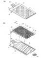
図1(A)は、本発明の一態様のタッチパネルモジュール10の斜視概略図である。図1(B)は、タッチパネルモジュール10の分解斜視概略図である。タッチパネルモジュール10は、基板31と基板21とが貼り合わされた構成を有する。タッチセンサ22は、基板21側に設けられている。基板31には、表示パネルを構成する回路が設けられている。
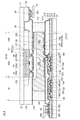
図5は、タッチパネルモジュール10の断面構造の概略図である。ここでは、図5に示すタッチパネルモジュール10を「タッチパネルモジュール10―1」と呼ぶこととする。
図6に示すタッチパネルモジュール10−2では、電極23、24を形成した後、カラーフィルタを設けている。絶縁層121、電極23、24を覆って、絶縁層131が設けられている。絶縁層131上にカラーフィルタを構成する着色層が設けられる。副画素の表示色に合わせて層CR、層CB、層CGの何れか1層が設けられる。カラーフィルタを覆って絶縁層122が形成される。絶縁層122上に電極25、26が設けられている。なお、絶縁層131は設けずに、電極23、24上にカラーフィルタを設けてもよい。
図7に示すタッチパネルモジュール10−3では、電極25、26の上方にカラーフィルタが設けられている。具体的には、絶縁層123上にカラーフィルタを構成する着色層が設けられている。副画素の表示色に合わせて、部位22Bの絶縁層122上に層CR、層CB、層CGの何れか1層が設けられる。カラーフィルタを覆って絶縁層124が形成されている。
図8に示すタッチパネルモジュール10−4は、タッチパネルモジュール10−3の変形例であり、絶縁層130上にカラーフィルタを構成する着色層が設けられている。副画素の表示色に合わせて、絶縁層130上に層CR、層CB、層CGの何れか1層が設けられる。カラーフィルタ、電極25、26を覆って、絶縁層123が設けられている。なお、部位22Bにでもカラーフィルタが存在しない領域がある。
図9に示すタッチパネルモジュール10−5では、電極25、26の形成前にカラーフィルタが形成される。絶縁層122上にカラーフィルタが設けられている。副画素の表示色に合わせて、絶縁層122上に層CR、層CB、層CGの何れか1層が設けられる。部位22Aには、絶縁層122上に、電極25が設けられている。部位22Bには、層CR上に電極26が設けられている。なお、部位22Bのカラーフィルタが存在しない領域では、電極26は絶縁層122上面と接することとなる。
図10に示すタッチパネルモジュール10−6は、タッチパネルモジュール10−5と同様に、電極25、26の形成前にカラーフィルタが形成される。タッチパネルモジュール10−6では、絶縁層123の形成後に、電極25、26を形成している点で、タッチパネルモジュール10−5と異なる。電極25が設けられる部位の絶縁層123は除去される。つまり、電極25は絶縁層123の開口の内の絶縁層122上に設けられ、電極26は絶縁層123上に設けられる。
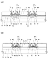
本実施の形態では、タッチパネルモジュール10に適用可能なトランジスタについて説明する。
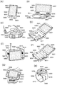
本実施の形態では、本発明の一態様の表示装置、または表示システムを有する表示モジュール及び電子機器について、図17及び図18を用いて説明を行う。
20 タッチパネル
21 基板
22 タッチセンサ
22A、22B 部位
23 電極
23a 配線
23A 電極
24 電極
24a 配線
24A 電極
24b 中継配線
25 電極
26 電極
27 絶縁層
27a 開口
28 電極
29 配線
31 基板
32 表示部
33 画素
121―124、130、131 絶縁層
141 接着層
150 液晶層
151 導電層
152 導電層
155 半導体層
160 ブラックマトリクス(BM)
161、162 導電膜
162a 開口
180 チャネル形成領域
181 低濃度不純物領域
182 高濃度不純物領域
185 スペーサ
190 チャネル形成領域
192 高濃度不純物領域
210 絶縁層
210−215 絶縁層
215 絶縁層
220―222、241、242 導電層
243 端子
Claims (3)
- 第1基板、第2基板、液晶層、画素電極、コモン電極、および、タッチセンサを有し、
前記第1基板は、前記第2基板と対向し、
前記液晶層は、前記第1基板と前記第2基板との間に設けられ、
前記画素電極および前記コモン電極は、前記第1基板に設けられ、
前記画素電極と前記コモン電極との間の電界によって、前記液晶層の配向を制御するタッチパネルであって、
前記タッチセンサは、前記第2基板に設けられ、
前記タッチセンサは、第1電極、2つの第2電極、および、第3電極を有し、
前記第1電極と前記第2電極とは、第1導電膜から形成され、
前記第3電極と第4電極とは、第2導電膜から形成され、
前記第4電極は、前記第3電極と離間し、且つ、前記第3電極の周囲を囲むように配置され、
前記第1電極と前記第2電極とは、複数の開口を有するメッシュ状の電極であり、
前記第1電極は、第1方向に延伸し、
2つの前記第2電極は、前記第1電極を挟んで第2方向に沿って設けられ、
2つの前記第2電極は、前記第3電極によって電気的に接続され、
前記第3電極は、前記第1電極と重なる領域を有し、
前記第4電極は、前記液晶層を挟んで、前記画素電極および前記コモン電極と対向するように設けられているタッチパネル。 - 第1基板、第2基板、液晶層、画素電極、コモン電極、および、タッチセンサを有し、
前記第1基板は、前記第2基板と対向し、
前記液晶層は、前記第1基板と前記第2基板との間に設けられ、
前記画素電極および前記コモン電極は、前記第1基板に設けられ、
前記画素電極と前記コモン電極との間の電界によって、前記液晶層の配向を制御するタッチパネルであって、
前記タッチセンサは、前記第2基板に設けられ、
前記タッチセンサは、第1電極、2つの第2電極、および、第3電極を有し、
前記第3電極と第4電極とは、同じ導電膜から形成され、
前記第4電極は、前記第3電極と離間し、且つ、前記第3電極の周囲を囲むように配置され、
2つの前記第2電極は、前記第3電極によって電気的に接続され、
前記第3電極は、前記第1電極と重なる領域を有し、
前記第4電極は、前記液晶層を挟んで、前記画素電極および前記コモン電極と対向するように設けられているタッチパネル。 - 請求項1又は請求項2において、
前記第1基板は、トランジスタと、絶縁膜と、を有し、
前記画素電極は、前記絶縁膜に設けられた開口部を介して前記トランジスタのソース又はドレインと電気的に接続され、
前記第3電極は、前記トランジスタのチャネル形成領域と重なる領域と、前記開口部と重なる領域と、を有するタッチパネル。
Applications Claiming Priority (2)
| Application Number | Priority Date | Filing Date | Title |
|---|---|---|---|
| JP2015060598 | 2015-03-24 | ||
| JP2015060598 | 2015-03-24 |
Publications (3)
| Publication Number | Publication Date |
|---|---|
| JP2016181261A JP2016181261A (ja) | 2016-10-13 |
| JP2016181261A5 JP2016181261A5 (ja) | 2019-05-09 |
| JP6711657B2 true JP6711657B2 (ja) | 2020-06-17 |
Family
ID=56975296
Family Applications (1)
| Application Number | Title | Priority Date | Filing Date |
|---|---|---|---|
| JP2016059490A Active JP6711657B2 (ja) | 2015-03-24 | 2016-03-24 | タッチパネル |
Country Status (5)
| Country | Link |
|---|---|
| US (1) | US10095362B2 (ja) |
| JP (1) | JP6711657B2 (ja) |
| KR (1) | KR20160114510A (ja) |
| CN (1) | CN106019664B (ja) |
| TW (1) | TWI693539B (ja) |
Families Citing this family (38)
| Publication number | Priority date | Publication date | Assignee | Title |
|---|---|---|---|---|
| KR20160114510A (ko) * | 2015-03-24 | 2016-10-05 | 가부시키가이샤 한도오따이 에네루기 켄큐쇼 | 터치 패널 |
| US10671204B2 (en) | 2015-05-04 | 2020-06-02 | Semiconductor Energy Laboratory Co., Ltd. | Touch panel and data processor |
| US20160328061A1 (en) * | 2015-05-07 | 2016-11-10 | Raydium Semiconductor Corporation | In-cell touch panel |
| US20160334660A1 (en) * | 2015-05-15 | 2016-11-17 | Raydium Semiconductor Corporation | In-cell touch panel |
| US10684500B2 (en) | 2015-05-27 | 2020-06-16 | Semiconductor Energy Laboratory Co., Ltd. | Touch panel |
| US10613690B2 (en) | 2015-05-28 | 2020-04-07 | Semiconductor Energy Laboratory Co., Ltd. | Touch panel |
| JP2017003976A (ja) | 2015-06-15 | 2017-01-05 | 株式会社半導体エネルギー研究所 | 表示装置 |
| KR102418492B1 (ko) * | 2015-06-30 | 2022-07-06 | 엘지디스플레이 주식회사 | 플렉서블 유기발광표시패널 |
| KR101750428B1 (ko) * | 2015-09-24 | 2017-06-23 | 엘지디스플레이 주식회사 | 터치 스크린 일체형 표시장치 |
| WO2017062743A1 (en) | 2015-10-07 | 2017-04-13 | Board Of Supervisors Of Louisiana State University And Agricultural And Mechanical College | Self-powered lights for photosynthetic cultures |
| CN105629548A (zh) * | 2016-01-26 | 2016-06-01 | 京东方科技集团股份有限公司 | 显示基板及其制作方法和显示装置 |
| US20170229554A1 (en) * | 2016-02-05 | 2017-08-10 | Applied Materials, Inc. | High-k dielectric materials utilized in display devices |
| KR102651542B1 (ko) * | 2016-06-17 | 2024-03-28 | 삼성전자주식회사 | 터치-지문 복합 센서를 포함하는 전자 기기 |
| KR102365490B1 (ko) | 2016-07-13 | 2022-02-18 | 가부시키가이샤 한도오따이 에네루기 켄큐쇼 | 입출력 패널, 입출력 장치, 반도체 장치 |
| JP6756538B2 (ja) * | 2016-08-03 | 2020-09-16 | 株式会社ジャパンディスプレイ | 表示装置 |
| CN108022565B (zh) * | 2016-11-02 | 2021-03-30 | 群创光电股份有限公司 | 调整方法以及显示器 |
| JP7050460B2 (ja) | 2016-11-22 | 2022-04-08 | 株式会社半導体エネルギー研究所 | 表示装置 |
| KR102668136B1 (ko) | 2016-12-12 | 2024-05-24 | 삼성디스플레이 주식회사 | 표시모듈 |
| KR102793060B1 (ko) * | 2016-12-16 | 2025-04-08 | 엘지디스플레이 주식회사 | 표시 장치 및 그 제조 방법 |
| KR102662681B1 (ko) | 2016-12-26 | 2024-04-30 | 엘지디스플레이 주식회사 | 터치 스크린 일체형 표시장치와 그의 제조방법 |
| KR102716926B1 (ko) | 2016-12-26 | 2024-10-11 | 엘지디스플레이 주식회사 | 터치 스크린 일체형 표시장치 |
| JP6842362B2 (ja) * | 2017-05-12 | 2021-03-17 | 株式会社ジャパンディスプレイ | 表示装置 |
| TWI615765B (zh) * | 2017-06-12 | 2018-02-21 | 友達光電股份有限公司 | 觸控感測基板以及整合偏光與觸控功能之結構 |
| TWI652606B (zh) * | 2017-06-29 | 2019-03-01 | 日商阿爾普士電氣股份有限公司 | Input device |
| KR102419557B1 (ko) * | 2017-08-28 | 2022-07-08 | 엘지디스플레이 주식회사 | 터치 스크린 패널 및 이를 포함하는 표시 장치 |
| KR102481250B1 (ko) * | 2018-03-08 | 2022-12-26 | 삼성디스플레이 주식회사 | 표시 장치 |
| JP6576498B2 (ja) * | 2018-03-09 | 2019-09-18 | Nissha株式会社 | Fpc一体型静電容量スイッチおよびその製造方法 |
| TWI693679B (zh) * | 2018-08-07 | 2020-05-11 | 矽品精密工業股份有限公司 | 電子封裝件 |
| KR102883426B1 (ko) * | 2019-07-30 | 2025-11-07 | 엘지디스플레이 주식회사 | 터치 디스플레이 장치 |
| CN111163214B (zh) * | 2019-12-11 | 2022-03-11 | 维沃移动通信有限公司 | 控制方法及电子设备 |
| WO2021147895A1 (en) * | 2020-01-20 | 2021-07-29 | So Tak Ching | An electrode for an electronic device, a method for fabricating an electrode for an electronic device and a pixelated smartfilm apparatus |
| US11079879B1 (en) * | 2020-01-22 | 2021-08-03 | Wuhan China Star Optoelectronics Semiconductor Display Technology Co., Ltd. | Flexible touch display device |
| CN113285041B (zh) * | 2020-02-20 | 2023-12-08 | 京东方科技集团股份有限公司 | 显示基板及其制作方法、显示装置 |
| KR20220008997A (ko) * | 2020-07-14 | 2022-01-24 | 삼성디스플레이 주식회사 | 전자장치 |
| KR102461794B1 (ko) * | 2020-08-13 | 2022-11-02 | 한국과학기술연구원 | 은 나노와이어 메쉬 전극 및 이의 제조방법 |
| CN112968046B (zh) * | 2021-02-09 | 2022-11-29 | 湖北长江新型显示产业创新中心有限公司 | 一种显示面板和显示装置 |
| US12248650B2 (en) * | 2022-01-26 | 2025-03-11 | Chengdu Boe Optoelectronics Technology Co., Ltd. | Touch structure, touch display panel and display device |
| CN114690492A (zh) * | 2022-03-16 | 2022-07-01 | 武汉华星光电技术有限公司 | 显示面板及显示终端 |
Family Cites Families (75)
| Publication number | Priority date | Publication date | Assignee | Title |
|---|---|---|---|---|
| US6690437B2 (en) * | 2000-04-18 | 2004-02-10 | Semiconductor Energy Laboratory Co., Ltd. | Electro-optical device |
| CN1410806A (zh) * | 2001-09-25 | 2003-04-16 | 瀚宇彩晶股份有限公司 | Odf液晶面板的制造方法 |
| JP4507480B2 (ja) | 2001-12-27 | 2010-07-21 | ソニー株式会社 | 表示装置 |
| CN1584636A (zh) * | 2003-08-21 | 2005-02-23 | 广辉电子股份有限公司 | 彩色滤光片及其制作方法 |
| US7433004B2 (en) * | 2004-06-11 | 2008-10-07 | Sharp Kabushiki Kaisha | Color filter substrate, method of making the color filter substrate and display device including the color filter substrate |
| JP2007226175A (ja) * | 2006-01-26 | 2007-09-06 | Epson Imaging Devices Corp | 液晶装置及び電子機器 |
| TWI322374B (en) * | 2006-04-14 | 2010-03-21 | Ritdisplay Corp | Light transmission touch panel and manufacturing method thereof |
| US8243027B2 (en) | 2006-06-09 | 2012-08-14 | Apple Inc. | Touch screen liquid crystal display |
| JP5154316B2 (ja) * | 2008-06-30 | 2013-02-27 | 株式会社ジャパンディスプレイイースト | タッチパネル |
| KR101500425B1 (ko) * | 2008-08-27 | 2015-03-09 | 삼성디스플레이 주식회사 | 터치 스크린 표시 장치 |
| KR101513440B1 (ko) * | 2008-12-01 | 2015-04-22 | 삼성디스플레이 주식회사 | 터치 스크린 표시 장치 및 그 제조 방법 |
| TWI633371B (zh) * | 2008-12-03 | 2018-08-21 | 半導體能源研究所股份有限公司 | 液晶顯示裝置 |
| US8461582B2 (en) * | 2009-03-05 | 2013-06-11 | Semiconductor Energy Laboratory Co., Ltd. | Semiconductor device and method for manufacturing the same |
| CN101989160A (zh) * | 2009-08-07 | 2011-03-23 | 铼宝科技股份有限公司 | 电容式触控面板 |
| JP5439114B2 (ja) * | 2009-10-21 | 2014-03-12 | 株式会社ジャパンディスプレイ | 静電容量型入力装置および入力装置付き電気光学装置 |
| JP5537915B2 (ja) * | 2009-12-01 | 2014-07-02 | 株式会社ジャパンディスプレイ | タッチパネル |
| TW201124766A (en) * | 2010-01-08 | 2011-07-16 | Wintek Corp | Display device with touch panel |
| KR101298234B1 (ko) * | 2010-03-19 | 2013-08-22 | 엘지디스플레이 주식회사 | 터치인식 횡전계형 액정표시장치 및 이의 제조 방법 |
| TWI441119B (zh) * | 2010-04-02 | 2014-06-11 | Arolltech Co Ltd | 具內嵌觸控裝置之顯示器 |
| US10088930B2 (en) * | 2011-11-25 | 2018-10-02 | Shanghai Tianma Micro-electronics Co., Ltd. | Active matrix organic light emitting diode in-cell touch panel and drive method thereof |
| KR101524449B1 (ko) * | 2011-12-22 | 2015-06-02 | 엘지디스플레이 주식회사 | 액정표시장치 및 그 제조방법 |
| KR101466556B1 (ko) * | 2012-03-29 | 2014-11-28 | 엘지디스플레이 주식회사 | 액정표시장치 및 그 제조방법 |
| KR101944503B1 (ko) * | 2012-06-21 | 2019-04-18 | 삼성디스플레이 주식회사 | 센서 기판 및 이를 포함하는 센싱 표시 패널 |
| KR102114212B1 (ko) * | 2012-08-10 | 2020-05-22 | 가부시키가이샤 한도오따이 에네루기 켄큐쇼 | 표시 장치 |
| KR101968929B1 (ko) * | 2012-09-11 | 2019-04-16 | 삼성디스플레이 주식회사 | 센서 기판, 이의 제조 방법 및 이를 포함하는 센싱 표시 패널 |
| US9389737B2 (en) * | 2012-09-14 | 2016-07-12 | Samsung Display Co., Ltd. | Display device and method of driving the same in two modes |
| KR102029437B1 (ko) * | 2012-12-17 | 2019-10-07 | 엘지디스플레이 주식회사 | 터치센서 일체형 표시장치 |
| KR20140080038A (ko) * | 2012-12-20 | 2014-06-30 | 삼성전기주식회사 | 터치패널 및 그 제조방법 |
| TW201426444A (zh) * | 2012-12-27 | 2014-07-01 | Wintek Corp | 觸控顯示裝置 |
| KR102057666B1 (ko) * | 2013-02-19 | 2019-12-23 | 삼성디스플레이 주식회사 | 터치 스크린 패널 및 그 제조 방법 |
| US9417475B2 (en) * | 2013-02-22 | 2016-08-16 | Semiconductor Energy Laboratory Co., Ltd. | Display device |
| KR102141459B1 (ko) * | 2013-03-22 | 2020-08-05 | 가부시키가이샤 한도오따이 에네루기 켄큐쇼 | 액정 표시 장치 |
| TWI636309B (zh) * | 2013-07-25 | 2018-09-21 | 日商半導體能源研究所股份有限公司 | 液晶顯示裝置及電子裝置 |
| JP6396478B2 (ja) * | 2013-09-27 | 2018-09-26 | センセル インコーポレイテッドSensel,Inc. | タッチセンサ検出システム及び方法 |
| KR102112090B1 (ko) * | 2013-10-23 | 2020-05-18 | 엘지디스플레이 주식회사 | 터치 센서 일체형 표시장치 |
| KR102098386B1 (ko) * | 2013-10-24 | 2020-04-07 | 엘지이노텍 주식회사 | 터치 패널 |
| KR102239367B1 (ko) * | 2013-11-27 | 2021-04-09 | 가부시키가이샤 한도오따이 에네루기 켄큐쇼 | 터치 패널 |
| JP2015125224A (ja) * | 2013-12-26 | 2015-07-06 | 株式会社ジャパンディスプレイ | 液晶表示装置 |
| JP6320227B2 (ja) * | 2014-01-17 | 2018-05-09 | 株式会社ジャパンディスプレイ | 表示装置 |
| JP2015143933A (ja) * | 2014-01-31 | 2015-08-06 | 株式会社ジャパンディスプレイ | 静電容量型センサ付き表示装置及びその駆動方法 |
| WO2015132694A1 (en) * | 2014-03-07 | 2015-09-11 | Semiconductor Energy Laboratory Co., Ltd. | Touch sensor, touch panel, and manufacturing method of touch panel |
| CN104915077B (zh) * | 2014-03-13 | 2017-11-28 | 乐金显示有限公司 | 触摸感应显示装置 |
| KR102187807B1 (ko) * | 2014-04-17 | 2020-12-07 | 엘지이노텍 주식회사 | 터치 패널 및 이를 포함하는 터치 디바이스 |
| WO2015162522A1 (en) | 2014-04-23 | 2015-10-29 | Semiconductor Energy Laboratory Co., Ltd. | Input/output device and method for driving input/output device |
| JP6518133B2 (ja) | 2014-05-30 | 2019-05-22 | 株式会社半導体エネルギー研究所 | 入力装置 |
| TWI790965B (zh) * | 2014-05-30 | 2023-01-21 | 日商半導體能源研究所股份有限公司 | 觸控面板 |
| US9455281B2 (en) * | 2014-06-19 | 2016-09-27 | Semiconductor Energy Laboratory Co., Ltd. | Touch sensor, touch panel, touch panel module, and display device |
| JP5813836B1 (ja) * | 2014-08-22 | 2015-11-17 | 日本航空電子工業株式会社 | 静電容量式タッチパネル |
| US10209841B2 (en) * | 2014-09-10 | 2019-02-19 | Sharp Kabushiki Kaisha | Position inputting device and display device with position inputting function |
| KR102240937B1 (ko) * | 2014-10-10 | 2021-04-15 | 삼성디스플레이 주식회사 | 표시 장치 |
| KR102500994B1 (ko) * | 2014-10-17 | 2023-02-16 | 가부시키가이샤 한도오따이 에네루기 켄큐쇼 | 터치 패널 |
| KR102299875B1 (ko) * | 2014-11-07 | 2021-09-07 | 엘지디스플레이 주식회사 | 터치 패널, 이의 제조 방법 및 터치 패널 일체형 유기 발광 표시 장치 |
| JP2016095502A (ja) * | 2014-11-11 | 2016-05-26 | 株式会社半導体エネルギー研究所 | 表示システム、表示装置 |
| US9933872B2 (en) * | 2014-12-01 | 2018-04-03 | Semiconductor Energy Laboratory Co., Ltd. | Touch panel |
| US20160253024A1 (en) * | 2015-02-27 | 2016-09-01 | Panasonic Liquid Crystal Display Co., Ltd. | Display panel with touch detection function |
| JP6765199B2 (ja) * | 2015-03-17 | 2020-10-07 | 株式会社半導体エネルギー研究所 | タッチパネル |
| WO2016147074A1 (en) * | 2015-03-17 | 2016-09-22 | Semiconductor Energy Laboratory Co., Ltd. | Touch panel |
| KR20160114510A (ko) * | 2015-03-24 | 2016-10-05 | 가부시키가이샤 한도오따이 에네루기 켄큐쇼 | 터치 패널 |
| US10684500B2 (en) * | 2015-05-27 | 2020-06-16 | Semiconductor Energy Laboratory Co., Ltd. | Touch panel |
| US10139663B2 (en) * | 2015-05-29 | 2018-11-27 | Semiconductor Energy Laboratory Co., Ltd. | Input/output device and electronic device |
| JP2017003976A (ja) * | 2015-06-15 | 2017-01-05 | 株式会社半導体エネルギー研究所 | 表示装置 |
| JP6532336B2 (ja) * | 2015-07-24 | 2019-06-19 | 三菱電機株式会社 | 表示装置 |
| CN106409919A (zh) * | 2015-07-30 | 2017-02-15 | 株式会社半导体能源研究所 | 半导体装置以及包括该半导体装置的显示装置 |
| CN105183251A (zh) * | 2015-08-10 | 2015-12-23 | 深圳市华星光电技术有限公司 | 一种具有触控功能的阵列基板及显示装置 |
| KR102375275B1 (ko) * | 2015-09-10 | 2022-03-18 | 삼성디스플레이 주식회사 | 터치 스크린 일체형 표시장치 및 그의 제조방법 |
| CN105159515B (zh) * | 2015-09-18 | 2018-09-07 | 京东方科技集团股份有限公司 | 触控结构及其制作方法、触控基板和显示装置 |
| US20170104090A1 (en) * | 2015-10-12 | 2017-04-13 | Semiconductor Energy Laboratory Co., Ltd. | Method for manufacturing semiconductor device |
| JP6539190B2 (ja) * | 2015-11-20 | 2019-07-03 | 株式会社ジャパンディスプレイ | タッチ検出装置及びタッチ検出機能付き表示装置 |
| KR102480270B1 (ko) * | 2015-12-11 | 2022-12-23 | 주식회사 지2터치 | 터치스크린 내장형 표시 장치 및 터치 검출 방법 |
| KR102513362B1 (ko) * | 2015-12-11 | 2023-03-24 | 삼성디스플레이 주식회사 | 액정 표시 패널 및 이의 제조 방법 |
| KR101725298B1 (ko) * | 2015-12-11 | 2017-04-10 | 주식회사 지2터치 | 터치스크린 내장형 표시 장치 및 그 제조 방법 |
| CN105677092B (zh) * | 2016-01-04 | 2019-05-10 | 京东方科技集团股份有限公司 | 面板及其制作方法和显示装置 |
| CN108780256B (zh) * | 2016-03-15 | 2022-10-18 | 株式会社半导体能源研究所 | 显示装置、模块及电子设备 |
| JP2017198729A (ja) * | 2016-04-25 | 2017-11-02 | 株式会社ジャパンディスプレイ | 表示装置 |
| KR102470044B1 (ko) * | 2016-05-13 | 2022-11-24 | 삼성디스플레이 주식회사 | 플렉서블 표시 장치 및 이의 제조 방법 |
-
2016
- 2016-03-17 KR KR1020160031852A patent/KR20160114510A/ko not_active Ceased
- 2016-03-18 TW TW105108493A patent/TWI693539B/zh not_active IP Right Cessation
- 2016-03-22 US US15/076,950 patent/US10095362B2/en active Active
- 2016-03-24 CN CN201610171585.2A patent/CN106019664B/zh not_active Expired - Fee Related
- 2016-03-24 JP JP2016059490A patent/JP6711657B2/ja active Active
Also Published As
| Publication number | Publication date |
|---|---|
| TW201643654A (zh) | 2016-12-16 |
| TWI693539B (zh) | 2020-05-11 |
| US10095362B2 (en) | 2018-10-09 |
| US20160282989A1 (en) | 2016-09-29 |
| KR20160114510A (ko) | 2016-10-05 |
| JP2016181261A (ja) | 2016-10-13 |
| CN106019664B (zh) | 2020-12-22 |
| CN106019664A (zh) | 2016-10-12 |
Similar Documents
| Publication | Publication Date | Title |
|---|---|---|
| JP6711657B2 (ja) | タッチパネル | |
| JP7622275B2 (ja) | 表示装置及び発光装置 | |
| JP2025016495A (ja) | 半導体装置 | |
| JP7417649B2 (ja) | 表示装置 | |
| JP6713820B2 (ja) | タッチパネル | |
| JP2025148503A (ja) | 表示装置 |
Legal Events
| Date | Code | Title | Description |
|---|---|---|---|
| A521 | Request for written amendment filed |
Free format text: JAPANESE INTERMEDIATE CODE: A523 Effective date: 20190322 |
|
| A621 | Written request for application examination |
Free format text: JAPANESE INTERMEDIATE CODE: A621 Effective date: 20190322 |
|
| A977 | Report on retrieval |
Free format text: JAPANESE INTERMEDIATE CODE: A971007 Effective date: 20191113 |
|
| A131 | Notification of reasons for refusal |
Free format text: JAPANESE INTERMEDIATE CODE: A131 Effective date: 20191210 |
|
| A521 | Request for written amendment filed |
Free format text: JAPANESE INTERMEDIATE CODE: A523 Effective date: 20200128 |
|
| TRDD | Decision of grant or rejection written | ||
| A01 | Written decision to grant a patent or to grant a registration (utility model) |
Free format text: JAPANESE INTERMEDIATE CODE: A01 Effective date: 20200512 |
|
| A61 | First payment of annual fees (during grant procedure) |
Free format text: JAPANESE INTERMEDIATE CODE: A61 Effective date: 20200528 |
|
| R150 | Certificate of patent or registration of utility model |
Ref document number: 6711657 Country of ref document: JP Free format text: JAPANESE INTERMEDIATE CODE: R150 |
|
| R250 | Receipt of annual fees |
Free format text: JAPANESE INTERMEDIATE CODE: R250 |
|
| R250 | Receipt of annual fees |
Free format text: JAPANESE INTERMEDIATE CODE: R250 |
|
| R250 | Receipt of annual fees |
Free format text: JAPANESE INTERMEDIATE CODE: R250 |