JP6733425B2 - 半導体集積回路及び半導体モジュール - Google Patents
半導体集積回路及び半導体モジュール Download PDFInfo
- Publication number
- JP6733425B2 JP6733425B2 JP2016166804A JP2016166804A JP6733425B2 JP 6733425 B2 JP6733425 B2 JP 6733425B2 JP 2016166804 A JP2016166804 A JP 2016166804A JP 2016166804 A JP2016166804 A JP 2016166804A JP 6733425 B2 JP6733425 B2 JP 6733425B2
- Authority
- JP
- Japan
- Prior art keywords
- well region
- region
- layer
- semiconductor substrate
- integrated circuit
- Prior art date
- Legal status (The legal status is an assumption and is not a legal conclusion. Google has not performed a legal analysis and makes no representation as to the accuracy of the status listed.)
- Expired - Fee Related
Links
Images


Classifications
-
- H—ELECTRICITY
- H03—ELECTRONIC CIRCUITRY
- H03K—PULSE TECHNIQUE
- H03K17/00—Electronic switching or gating, i.e. not by contact-making and –breaking
- H03K17/51—Electronic switching or gating, i.e. not by contact-making and –breaking characterised by the components used
- H03K17/56—Electronic switching or gating, i.e. not by contact-making and –breaking characterised by the components used by the use, as active elements, of semiconductor devices
- H03K17/687—Electronic switching or gating, i.e. not by contact-making and –breaking characterised by the components used by the use, as active elements, of semiconductor devices the devices being field-effect transistors
- H03K17/6871—Electronic switching or gating, i.e. not by contact-making and –breaking characterised by the components used by the use, as active elements, of semiconductor devices the devices being field-effect transistors the output circuit comprising more than one controlled field-effect transistor
- H03K17/6872—Electronic switching or gating, i.e. not by contact-making and –breaking characterised by the components used by the use, as active elements, of semiconductor devices the devices being field-effect transistors the output circuit comprising more than one controlled field-effect transistor using complementary field-effect transistors
-
- H—ELECTRICITY
- H10—SEMICONDUCTOR DEVICES; ELECTRIC SOLID-STATE DEVICES NOT OTHERWISE PROVIDED FOR
- H10D—INORGANIC ELECTRIC SEMICONDUCTOR DEVICES
- H10D30/00—Field-effect transistors [FET]
- H10D30/60—Insulated-gate field-effect transistors [IGFET]
- H10D30/64—Double-diffused metal-oxide semiconductor [DMOS] FETs
- H10D30/65—Lateral DMOS [LDMOS] FETs
-
- H—ELECTRICITY
- H10—SEMICONDUCTOR DEVICES; ELECTRIC SOLID-STATE DEVICES NOT OTHERWISE PROVIDED FOR
- H10D—INORGANIC ELECTRIC SEMICONDUCTOR DEVICES
- H10D62/00—Semiconductor bodies, or regions thereof, of devices having potential barriers
- H10D62/10—Shapes, relative sizes or dispositions of the regions of the semiconductor bodies; Shapes of the semiconductor bodies
- H10D62/113—Isolations within a component, i.e. internal isolations
- H10D62/115—Dielectric isolations, e.g. air gaps
-
- H—ELECTRICITY
- H10—SEMICONDUCTOR DEVICES; ELECTRIC SOLID-STATE DEVICES NOT OTHERWISE PROVIDED FOR
- H10D—INORGANIC ELECTRIC SEMICONDUCTOR DEVICES
- H10D84/00—Integrated devices formed in or on semiconductor substrates that comprise only semiconducting layers, e.g. on Si wafers or on GaAs-on-Si wafers
- H10D84/80—Integrated devices formed in or on semiconductor substrates that comprise only semiconducting layers, e.g. on Si wafers or on GaAs-on-Si wafers characterised by the integration of at least one component covered by groups H10D12/00 or H10D30/00, e.g. integration of IGFETs
- H10D84/811—Combinations of field-effect devices and one or more diodes, capacitors or resistors
-
- H—ELECTRICITY
- H10—SEMICONDUCTOR DEVICES; ELECTRIC SOLID-STATE DEVICES NOT OTHERWISE PROVIDED FOR
- H10W—GENERIC PACKAGES, INTERCONNECTIONS, CONNECTORS OR OTHER CONSTRUCTIONAL DETAILS OF DEVICES COVERED BY CLASS H10
- H10W20/00—Interconnections in chips, wafers or substrates
- H10W20/01—Manufacture or treatment
- H10W20/031—Manufacture or treatment of conductive parts of the interconnections
- H10W20/069—Manufacture or treatment of conductive parts of the interconnections by forming self-aligned vias or self-aligned contact plugs
-
- H—ELECTRICITY
- H10—SEMICONDUCTOR DEVICES; ELECTRIC SOLID-STATE DEVICES NOT OTHERWISE PROVIDED FOR
- H10W—GENERIC PACKAGES, INTERCONNECTIONS, CONNECTORS OR OTHER CONSTRUCTIONAL DETAILS OF DEVICES COVERED BY CLASS H10
- H10W90/00—Package configurations
-
- H—ELECTRICITY
- H03—ELECTRONIC CIRCUITRY
- H03K—PULSE TECHNIQUE
- H03K2217/00—Indexing scheme related to electronic switching or gating, i.e. not by contact-making or -breaking covered by H03K17/00
- H03K2217/0063—High side switches, i.e. the higher potential [DC] or life wire [AC] being directly connected to the switch and not via the load
-
- H—ELECTRICITY
- H03—ELECTRONIC CIRCUITRY
- H03K—PULSE TECHNIQUE
- H03K2217/00—Indexing scheme related to electronic switching or gating, i.e. not by contact-making or -breaking covered by H03K17/00
- H03K2217/0072—Low side switches, i.e. the lower potential [DC] or neutral wire [AC] being directly connected to the switch and not via the load
-
- H—ELECTRICITY
- H10—SEMICONDUCTOR DEVICES; ELECTRIC SOLID-STATE DEVICES NOT OTHERWISE PROVIDED FOR
- H10D—INORGANIC ELECTRIC SEMICONDUCTOR DEVICES
- H10D84/00—Integrated devices formed in or on semiconductor substrates that comprise only semiconducting layers, e.g. on Si wafers or on GaAs-on-Si wafers
- H10D84/01—Manufacture or treatment
- H10D84/0123—Integrating together multiple components covered by H10D12/00 or H10D30/00, e.g. integrating multiple IGBTs
- H10D84/0126—Integrating together multiple components covered by H10D12/00 or H10D30/00, e.g. integrating multiple IGBTs the components including insulated gates, e.g. IGFETs
- H10D84/0165—Integrating together multiple components covered by H10D12/00 or H10D30/00, e.g. integrating multiple IGBTs the components including insulated gates, e.g. IGFETs the components including complementary IGFETs, e.g. CMOS devices
- H10D84/0191—Manufacturing their doped wells
-
- H—ELECTRICITY
- H10—SEMICONDUCTOR DEVICES; ELECTRIC SOLID-STATE DEVICES NOT OTHERWISE PROVIDED FOR
- H10D—INORGANIC ELECTRIC SEMICONDUCTOR DEVICES
- H10D84/00—Integrated devices formed in or on semiconductor substrates that comprise only semiconducting layers, e.g. on Si wafers or on GaAs-on-Si wafers
- H10D84/01—Manufacture or treatment
- H10D84/02—Manufacture or treatment characterised by using material-based technologies
- H10D84/03—Manufacture or treatment characterised by using material-based technologies using Group IV technology, e.g. silicon technology or silicon-carbide [SiC] technology
- H10D84/038—Manufacture or treatment characterised by using material-based technologies using Group IV technology, e.g. silicon technology or silicon-carbide [SiC] technology using silicon technology, e.g. SiGe
-
- H—ELECTRICITY
- H10—SEMICONDUCTOR DEVICES; ELECTRIC SOLID-STATE DEVICES NOT OTHERWISE PROVIDED FOR
- H10W—GENERIC PACKAGES, INTERCONNECTIONS, CONNECTORS OR OTHER CONSTRUCTIONAL DETAILS OF DEVICES COVERED BY CLASS H10
- H10W72/00—Interconnections or connectors in packages
- H10W72/071—Connecting or disconnecting
- H10W72/073—Connecting or disconnecting of die-attach connectors
- H10W72/07351—Connecting or disconnecting of die-attach connectors characterised by changes in properties of the die-attach connectors during connecting
-
- H—ELECTRICITY
- H10—SEMICONDUCTOR DEVICES; ELECTRIC SOLID-STATE DEVICES NOT OTHERWISE PROVIDED FOR
- H10W—GENERIC PACKAGES, INTERCONNECTIONS, CONNECTORS OR OTHER CONSTRUCTIONAL DETAILS OF DEVICES COVERED BY CLASS H10
- H10W72/00—Interconnections or connectors in packages
- H10W72/30—Die-attach connectors
Landscapes
- Metal-Oxide And Bipolar Metal-Oxide Semiconductor Integrated Circuits (AREA)
- Semiconductor Integrated Circuits (AREA)
Description
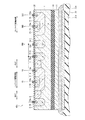
本発明の実施の形態に係る半導体集積回路40aは、比較的低容量のインバータ等において用いられるHVICであり、例えば600V〜1200V程度の電圧に耐えて動作する電力変換用ブリッジ回路の制御用ICである。半導体集積回路40aは、図1に示すように、低濃度の第1導電型(p−型)の半導体基板1と、図1中の左上側に示すように、この半導体基板1の上部に設けられた第2導電型(n型)の第1ウェル領域2と、を備える。
一方、比較例に係る半導体集積回路40zの場合、図8に示すように、半導体基板1と裏面電極層11の間に絶縁層10が設けられていない。そのため、負電圧サージの絶対値が大きいと、第1寄生ダイオードPD1及び第2寄生ダイオードPD2がオンし、第4経路R4、第5経路R5及び第6経路R6を介して、GND端子46側やVB端子44側へ流れる電流が大きくなる。
本発明は上記の開示した実施の形態によって説明したが、この開示の一部をなす論述及び図面は、本発明を限定するものであると理解すべきではない。この開示から当業者には様々な代替実施の形態、実施例及び運用技術が明らかになると考えられるべきである。
2 第1ウェル領域
3 第2ウェル領域
4 耐圧領域
5 第1分離領域
6a 第2分離領域
8 第1コンタクト領域
8a 第1コンタクト電極
10 絶縁層
11 裏面電極層
14 第2コンタクト領域
14a 第2コンタクト電極
15 第1分離コンタクト領域
15a 第1分離コンタクト電極
16 第2分離コンタクト領域
16a 第2分離コンタクト電極
20 層間絶縁膜
22 第3ウェル領域
23 第4ウェル領域
24 第4コンタクト領域
24a 第4コンタクト電極
28 第3コンタクト領域
28a 第3コンタクト電極
30 絶縁回路基板
31a〜31c 導体層
32a〜32c 接合層
40a〜40d,40z 半導体集積回路
41 入力端子
42 出力端子
43 VS端子
44 VB端子
45 VCC端子
46 GND端子
51 接続点
57 負荷
61 ソース領域
62 ドレイン領域
63 ソース電極
64 ドレイン電極
65 ゲート電極
71 ソース領域
72 ドレイン領域
73 ソース電極
74 ドレイン電極
75 ゲート電極
80 空乏層
FWD1〜FWD6 還流ダイオード
PD1 第1寄生ダイオード
PD2 第2寄生ダイオード
R1〜R6 第1経路〜第6経路
S1〜S6 スイッチング素子
d 距離
Claims (10)
- 第1導電型の半導体基板と、
前記半導体基板の上部に設けられた第2導電型の第1ウェル領域と、
前記第1ウェル領域の上部に設けられた第1導電型の第2ウェル領域と、
前記第1ウェル領域の直下の前記半導体基板の下部に前記第1ウェル領域から離間して設けられた絶縁層と、
前記絶縁層の下に設けられた裏面電極層と、を有し、
さらに、前記第1ウェル領域の上部に設けられた第1導電型の第1主電極領域及び第2主電極領域を有する第1能動素子と、前記第2ウェル領域の上部に設けられた第2導電型の第3主電極領域及び第4主電極領域を有する第2能動素子と、を備え、
前記第1能動素子及び前記第2能動素子によって、電力変換用ブリッジ回路のハイサイド駆動回路が構成されていることを特徴とする半導体集積回路。 - 前記半導体基板の上部に前記第1ウェル領域から離間して設けられ、かつ基準電位が印加される第1導電型の分離領域を更に備えることを特徴とする請求項1に記載の半導体集積回路。
- 第1導電型の半導体基板と、
前記半導体基板の上部に設けられた第2導電型の第1ウェル領域と、
前記第1ウェル領域の上部に設けられた第1導電型の第2ウェル領域と、
前記第1ウェル領域の直下の前記半導体基板の下部に前記第1ウェル領域から離間して設けられた絶縁層と、
前記絶縁層の下に設けられた裏面電極層と、を備え、
さらに、前記半導体基板の上部に前記第1ウェル領域から離間して設けられ、かつ基準電位が印加される第1導電型の分離領域を備えることを特徴とする半導体集積回路。 - 前記半導体基板の上部の前記第1ウェル領域と前記分離領域の間に設けられた第2導電型の耐圧領域を更に備えることを特徴とする請求項2又は請求項3に記載の半導体集積回路。
- 前記第1ウェル領域には第1電位が印加され、
前記第2ウェル領域には第1電位とは異なる第2電位が印加されることを特徴とする請求項1から請求項4のいずれか一項に記載の半導体集積回路。 - 前記第1ウェル領域と前記絶縁層との間の距離は、前記第1ウェル領域に前記第1電位を印加し、前記第2ウェル領域に第2電位を印加したときに、前記半導体基板と前記第1ウェル領域とのpn接合界面部から広がる空乏層が、前記絶縁層から離間する長さであることを特徴とする請求項5に記載の半導体集積回路。
- 第1導電型の半導体基板と、
前記半導体基板の上部に設けられた第2導電型の第1ウェル領域と、
前記第1ウェル領域の上部に設けられた第1導電型の第2ウェル領域と、
前記第1ウェル領域の直下の前記半導体基板の下部に前記第1ウェル領域から離間して設けられた絶縁層と、
前記絶縁層の下に設けられた裏面電極層と、を有する半導体集積回路と、
前記半導体集積回路を、表面に設けられた導電層の上に搭載する絶縁回路基板と、
前記導電層及び前記裏面電極層の間に介在し前記裏面電極層及び前記導電層を接合する接合層と、
を備えることを特徴とする半導体モジュール。 - 前記第1ウェル領域の上部に設けられた第1導電型の第1主電極領域及び第2主電極領域を有する第1能動素子と、
前記第2ウェル領域の上部に設けられた第2導電型の第3主電極領域及び第4主電極領域を有する第2能動素子と、
を更に備えることを特徴とする請求項7に記載の半導体モジュール。 - 前記絶縁回路基板の上に搭載され、前記第1能動素子及び前記第2能動素子によって駆動制御されるスイッチング素子を更に備えることを特徴とする請求項8に記載の半導体モジュール。
- 前記半導体集積回路及び前記スイッチング素子は、同じ高さで搭載されていることを特徴とする請求項9に記載の半導体モジュール。
Priority Applications (2)
| Application Number | Priority Date | Filing Date | Title |
|---|---|---|---|
| JP2016166804A JP6733425B2 (ja) | 2016-08-29 | 2016-08-29 | 半導体集積回路及び半導体モジュール |
| US15/641,604 US10121783B2 (en) | 2016-08-29 | 2017-07-05 | Semiconductor integrated circuit and semiconductor module |
Applications Claiming Priority (1)
| Application Number | Priority Date | Filing Date | Title |
|---|---|---|---|
| JP2016166804A JP6733425B2 (ja) | 2016-08-29 | 2016-08-29 | 半導体集積回路及び半導体モジュール |
Publications (2)
| Publication Number | Publication Date |
|---|---|
| JP2018037443A JP2018037443A (ja) | 2018-03-08 |
| JP6733425B2 true JP6733425B2 (ja) | 2020-07-29 |
Family
ID=61243458
Family Applications (1)
| Application Number | Title | Priority Date | Filing Date |
|---|---|---|---|
| JP2016166804A Expired - Fee Related JP6733425B2 (ja) | 2016-08-29 | 2016-08-29 | 半導体集積回路及び半導体モジュール |
Country Status (2)
| Country | Link |
|---|---|
| US (1) | US10121783B2 (ja) |
| JP (1) | JP6733425B2 (ja) |
Families Citing this family (3)
| Publication number | Priority date | Publication date | Assignee | Title |
|---|---|---|---|---|
| WO2021106941A1 (ja) * | 2019-11-25 | 2021-06-03 | アイシン・エィ・ダブリュ株式会社 | 制御基板 |
| JP7524665B2 (ja) * | 2020-08-12 | 2024-07-30 | 富士電機株式会社 | 半導体装置 |
| JP7848472B2 (ja) * | 2021-12-09 | 2026-04-21 | 富士電機株式会社 | 半導体装置 |
Family Cites Families (12)
| Publication number | Priority date | Publication date | Assignee | Title |
|---|---|---|---|---|
| JPH08335684A (ja) * | 1995-06-08 | 1996-12-17 | Toshiba Corp | 半導体装置 |
| JP2003280553A (ja) * | 2002-03-22 | 2003-10-02 | Sharp Corp | アクティブマトリクス基板 |
| JP4869546B2 (ja) * | 2003-05-23 | 2012-02-08 | ルネサスエレクトロニクス株式会社 | 半導体装置 |
| JP2006019612A (ja) * | 2004-07-05 | 2006-01-19 | Renesas Technology Corp | 半導体装置およびその製造方法 |
| JP2006179632A (ja) * | 2004-12-22 | 2006-07-06 | Fuji Electric Device Technology Co Ltd | 半導体装置およびその製造方法 |
| JP5151012B2 (ja) * | 2005-05-30 | 2013-02-27 | 富士電機株式会社 | 半導体装置の製造方法 |
| US8278719B2 (en) * | 2005-10-14 | 2012-10-02 | Silicon Space Technology Corp. | Radiation hardened isolation structures and fabrication methods |
| JP5537197B2 (ja) * | 2010-03-12 | 2014-07-02 | ルネサスエレクトロニクス株式会社 | 半導体装置の製造方法 |
| JP6008054B2 (ja) * | 2013-10-07 | 2016-10-19 | 富士電機株式会社 | 半導体装置 |
| JP6291792B2 (ja) | 2013-10-30 | 2018-03-14 | 富士電機株式会社 | 半導体装置およびその製造方法 |
| JP6337634B2 (ja) * | 2014-06-16 | 2018-06-06 | 富士電機株式会社 | 半導体集積回路装置 |
| WO2016132418A1 (ja) * | 2015-02-18 | 2016-08-25 | 富士電機株式会社 | 半導体集積回路 |
-
2016
- 2016-08-29 JP JP2016166804A patent/JP6733425B2/ja not_active Expired - Fee Related
-
2017
- 2017-07-05 US US15/641,604 patent/US10121783B2/en active Active
Also Published As
| Publication number | Publication date |
|---|---|
| JP2018037443A (ja) | 2018-03-08 |
| US20180061827A1 (en) | 2018-03-01 |
| US10121783B2 (en) | 2018-11-06 |
Similar Documents
| Publication | Publication Date | Title |
|---|---|---|
| TWI614877B (zh) | 半導體裝置 | |
| US11183485B2 (en) | Semiconductor module | |
| JP6743955B2 (ja) | 半導体集積回路の製造方法 | |
| JP6690336B2 (ja) | 半導体装置 | |
| JP2020174173A (ja) | 半導体集積回路 | |
| JP2019110162A (ja) | 半導体集積回路 | |
| JP6733425B2 (ja) | 半導体集積回路及び半導体モジュール | |
| JP2009206284A (ja) | 半導体装置 | |
| US9893065B2 (en) | Semiconductor integrated circuit | |
| US10727228B2 (en) | Stacked integrated circuit | |
| US10217765B2 (en) | Semiconductor integrated circuit | |
| JP2011199039A (ja) | 半導体装置 | |
| JP6729214B2 (ja) | 高耐圧集積回路装置および半導体装置 | |
| JP4513920B2 (ja) | 定電流制御回路 | |
| JP6641967B2 (ja) | 高耐圧集積回路装置 | |
| US11626878B2 (en) | Semiconductor device | |
| JP2025095538A (ja) | 半導体装置 | |
| JP2025082937A (ja) | 半導体装置 | |
| JP2024108876A (ja) | 半導体装置 | |
| JP2005340737A (ja) | モータ駆動用半導体装置 |
Legal Events
| Date | Code | Title | Description |
|---|---|---|---|
| RD03 | Notification of appointment of power of attorney |
Free format text: JAPANESE INTERMEDIATE CODE: A7423 Effective date: 20190411 |
|
| A621 | Written request for application examination |
Free format text: JAPANESE INTERMEDIATE CODE: A621 Effective date: 20190712 |
|
| RD04 | Notification of resignation of power of attorney |
Free format text: JAPANESE INTERMEDIATE CODE: A7424 Effective date: 20190726 |
|
| A977 | Report on retrieval |
Free format text: JAPANESE INTERMEDIATE CODE: A971007 Effective date: 20200310 |
|
| A131 | Notification of reasons for refusal |
Free format text: JAPANESE INTERMEDIATE CODE: A131 Effective date: 20200407 |
|
| A521 | Request for written amendment filed |
Free format text: JAPANESE INTERMEDIATE CODE: A523 Effective date: 20200520 |
|
| TRDD | Decision of grant or rejection written | ||
| A01 | Written decision to grant a patent or to grant a registration (utility model) |
Free format text: JAPANESE INTERMEDIATE CODE: A01 Effective date: 20200609 |
|
| A61 | First payment of annual fees (during grant procedure) |
Free format text: JAPANESE INTERMEDIATE CODE: A61 Effective date: 20200622 |
|
| R150 | Certificate of patent or registration of utility model |
Ref document number: 6733425 Country of ref document: JP Free format text: JAPANESE INTERMEDIATE CODE: R150 |
|
| R250 | Receipt of annual fees |
Free format text: JAPANESE INTERMEDIATE CODE: R250 |
|
| LAPS | Cancellation because of no payment of annual fees |