JP6740657B2 - インバータ装置 - Google Patents
インバータ装置 Download PDFInfo
- Publication number
- JP6740657B2 JP6740657B2 JP2016058909A JP2016058909A JP6740657B2 JP 6740657 B2 JP6740657 B2 JP 6740657B2 JP 2016058909 A JP2016058909 A JP 2016058909A JP 2016058909 A JP2016058909 A JP 2016058909A JP 6740657 B2 JP6740657 B2 JP 6740657B2
- Authority
- JP
- Japan
- Prior art keywords
- circuit
- switching element
- state
- turn
- current
- Prior art date
- Legal status (The legal status is an assumption and is not a legal conclusion. Google has not performed a legal analysis and makes no representation as to the accuracy of the status listed.)
- Active
Links
- 239000003990 capacitor Substances 0.000 claims description 62
- 230000007704 transition Effects 0.000 claims description 33
- 238000001514 detection method Methods 0.000 claims description 20
- 230000007423 decrease Effects 0.000 description 12
- 238000010586 diagram Methods 0.000 description 8
- 230000003111 delayed effect Effects 0.000 description 7
- 230000004044 response Effects 0.000 description 5
- 230000008859 change Effects 0.000 description 4
- 230000000052 comparative effect Effects 0.000 description 4
- 238000013016 damping Methods 0.000 description 4
- 230000000694 effects Effects 0.000 description 3
- 239000004065 semiconductor Substances 0.000 description 3
- PXHVJJICTQNCMI-UHFFFAOYSA-N Nickel Chemical compound [Ni] PXHVJJICTQNCMI-UHFFFAOYSA-N 0.000 description 2
- 230000008901 benefit Effects 0.000 description 2
- 238000007599 discharging Methods 0.000 description 2
- 230000007257 malfunction Effects 0.000 description 2
- 229910044991 metal oxide Inorganic materials 0.000 description 2
- 238000000034 method Methods 0.000 description 2
- 238000010992 reflux Methods 0.000 description 2
- 230000008929 regeneration Effects 0.000 description 2
- 238000011069 regeneration method Methods 0.000 description 2
- GYHNNYVSQQEPJS-UHFFFAOYSA-N Gallium Chemical compound [Ga] GYHNNYVSQQEPJS-UHFFFAOYSA-N 0.000 description 1
- UFHFLCQGNIYNRP-UHFFFAOYSA-N Hydrogen Chemical compound [H][H] UFHFLCQGNIYNRP-UHFFFAOYSA-N 0.000 description 1
- HBBGRARXTFLTSG-UHFFFAOYSA-N Lithium ion Chemical compound [Li+] HBBGRARXTFLTSG-UHFFFAOYSA-N 0.000 description 1
- XUIMIQQOPSSXEZ-UHFFFAOYSA-N Silicon Chemical compound [Si] XUIMIQQOPSSXEZ-UHFFFAOYSA-N 0.000 description 1
- 230000009471 action Effects 0.000 description 1
- 230000015556 catabolic process Effects 0.000 description 1
- 238000006243 chemical reaction Methods 0.000 description 1
- 238000002485 combustion reaction Methods 0.000 description 1
- 230000005669 field effect Effects 0.000 description 1
- 229910052733 gallium Inorganic materials 0.000 description 1
- 238000009499 grossing Methods 0.000 description 1
- 229910052739 hydrogen Inorganic materials 0.000 description 1
- 239000001257 hydrogen Substances 0.000 description 1
- 230000006698 induction Effects 0.000 description 1
- 229910001416 lithium ion Inorganic materials 0.000 description 1
- 238000004519 manufacturing process Methods 0.000 description 1
- 150000004706 metal oxides Chemical class 0.000 description 1
- 230000004048 modification Effects 0.000 description 1
- 238000012986 modification Methods 0.000 description 1
- 229910052759 nickel Inorganic materials 0.000 description 1
- 230000003071 parasitic effect Effects 0.000 description 1
- 238000002360 preparation method Methods 0.000 description 1
- 238000004904 shortening Methods 0.000 description 1
- 229910052710 silicon Inorganic materials 0.000 description 1
- 239000010703 silicon Substances 0.000 description 1
Images


Classifications
-
- H—ELECTRICITY
- H02—GENERATION; CONVERSION OR DISTRIBUTION OF ELECTRIC POWER
- H02P—CONTROL OR REGULATION OF ELECTRIC MOTORS, ELECTRIC GENERATORS OR DYNAMO-ELECTRIC CONVERTERS; CONTROLLING TRANSFORMERS, REACTORS OR CHOKE COILS
- H02P29/00—Arrangements for regulating or controlling electric motors, appropriate for both AC and DC motors
- H02P29/02—Providing protection against overload without automatic interruption of supply
- H02P29/032—Preventing damage to the motor, e.g. setting individual current limits for different drive conditions
-
- H—ELECTRICITY
- H02—GENERATION; CONVERSION OR DISTRIBUTION OF ELECTRIC POWER
- H02M—APPARATUS FOR CONVERSION BETWEEN AC AND AC, BETWEEN AC AND DC, OR BETWEEN DC AND DC, AND FOR USE WITH MAINS OR SIMILAR POWER SUPPLY SYSTEMS; CONVERSION OF DC OR AC INPUT POWER INTO SURGE OUTPUT POWER; CONTROL OR REGULATION THEREOF
- H02M1/00—Details of apparatus for conversion
- H02M1/08—Circuits specially adapted for the generation of control voltages for semiconductor devices incorporated in static converters
-
- H—ELECTRICITY
- H02—GENERATION; CONVERSION OR DISTRIBUTION OF ELECTRIC POWER
- H02M—APPARATUS FOR CONVERSION BETWEEN AC AND AC, BETWEEN AC AND DC, OR BETWEEN DC AND DC, AND FOR USE WITH MAINS OR SIMILAR POWER SUPPLY SYSTEMS; CONVERSION OF DC OR AC INPUT POWER INTO SURGE OUTPUT POWER; CONTROL OR REGULATION THEREOF
- H02M7/00—Conversion of AC power input into DC power output; Conversion of DC power input into AC power output
- H02M7/42—Conversion of DC power input into AC power output without possibility of reversal
- H02M7/44—Conversion of DC power input into AC power output without possibility of reversal by static converters
- H02M7/48—Conversion of DC power input into AC power output without possibility of reversal by static converters using discharge tubes with control electrode or semiconductor devices with control electrode
- H02M7/53—Conversion of DC power input into AC power output without possibility of reversal by static converters using discharge tubes with control electrode or semiconductor devices with control electrode using devices of a triode or transistor type requiring continuous application of a control signal
- H02M7/537—Conversion of DC power input into AC power output without possibility of reversal by static converters using discharge tubes with control electrode or semiconductor devices with control electrode using devices of a triode or transistor type requiring continuous application of a control signal using semiconductor devices only, e.g. single switched pulse inverters
- H02M7/5387—Conversion of DC power input into AC power output without possibility of reversal by static converters using discharge tubes with control electrode or semiconductor devices with control electrode using devices of a triode or transistor type requiring continuous application of a control signal using semiconductor devices only, e.g. single switched pulse inverters in a bridge configuration
-
- H—ELECTRICITY
- H02—GENERATION; CONVERSION OR DISTRIBUTION OF ELECTRIC POWER
- H02M—APPARATUS FOR CONVERSION BETWEEN AC AND AC, BETWEEN AC AND DC, OR BETWEEN DC AND DC, AND FOR USE WITH MAINS OR SIMILAR POWER SUPPLY SYSTEMS; CONVERSION OF DC OR AC INPUT POWER INTO SURGE OUTPUT POWER; CONTROL OR REGULATION THEREOF
- H02M7/00—Conversion of AC power input into DC power output; Conversion of DC power input into AC power output
- H02M7/66—Conversion of AC power input into DC power output; Conversion of DC power input into AC power output with possibility of reversal
- H02M7/68—Conversion of AC power input into DC power output; Conversion of DC power input into AC power output with possibility of reversal by static converters
- H02M7/72—Conversion of AC power input into DC power output; Conversion of DC power input into AC power output with possibility of reversal by static converters using discharge tubes with control electrode or semiconductor devices with control electrode
- H02M7/79—Conversion of AC power input into DC power output; Conversion of DC power input into AC power output with possibility of reversal by static converters using discharge tubes with control electrode or semiconductor devices with control electrode using devices of a triode or transistor type requiring continuous application of a control signal
- H02M7/797—Conversion of AC power input into DC power output; Conversion of DC power input into AC power output with possibility of reversal by static converters using discharge tubes with control electrode or semiconductor devices with control electrode using devices of a triode or transistor type requiring continuous application of a control signal using semiconductor devices only
-
- H—ELECTRICITY
- H02—GENERATION; CONVERSION OR DISTRIBUTION OF ELECTRIC POWER
- H02P—CONTROL OR REGULATION OF ELECTRIC MOTORS, ELECTRIC GENERATORS OR DYNAMO-ELECTRIC CONVERTERS; CONTROLLING TRANSFORMERS, REACTORS OR CHOKE COILS
- H02P29/00—Arrangements for regulating or controlling electric motors, appropriate for both AC and DC motors
- H02P29/02—Providing protection against overload without automatic interruption of supply
- H02P29/024—Detecting a fault condition, e.g. short circuit, locked rotor, open circuit or loss of load
- H02P29/026—Detecting a fault condition, e.g. short circuit, locked rotor, open circuit or loss of load the fault being a power fluctuation
-
- H—ELECTRICITY
- H03—ELECTRONIC CIRCUITRY
- H03K—PULSE TECHNIQUE
- H03K17/00—Electronic switching or gating, i.e. not by contact-making and –breaking
- H03K17/08—Modifications for protecting switching circuit against overcurrent or overvoltage
- H03K17/082—Modifications for protecting switching circuit against overcurrent or overvoltage by feedback from the output to the control circuit
- H03K17/0828—Modifications for protecting switching circuit against overcurrent or overvoltage by feedback from the output to the control circuit in composite switches
-
- H—ELECTRICITY
- H03—ELECTRONIC CIRCUITRY
- H03K—PULSE TECHNIQUE
- H03K17/00—Electronic switching or gating, i.e. not by contact-making and –breaking
- H03K17/16—Modifications for eliminating interference voltages or currents
- H03K17/161—Modifications for eliminating interference voltages or currents in field-effect transistor switches
- H03K17/162—Modifications for eliminating interference voltages or currents in field-effect transistor switches without feedback from the output circuit to the control circuit
- H03K17/163—Soft switching
-
- H—ELECTRICITY
- H03—ELECTRONIC CIRCUITRY
- H03K—PULSE TECHNIQUE
- H03K17/00—Electronic switching or gating, i.e. not by contact-making and –breaking
- H03K17/16—Modifications for eliminating interference voltages or currents
- H03K17/168—Modifications for eliminating interference voltages or currents in composite switches
-
- H—ELECTRICITY
- H02—GENERATION; CONVERSION OR DISTRIBUTION OF ELECTRIC POWER
- H02M—APPARATUS FOR CONVERSION BETWEEN AC AND AC, BETWEEN AC AND DC, OR BETWEEN DC AND DC, AND FOR USE WITH MAINS OR SIMILAR POWER SUPPLY SYSTEMS; CONVERSION OF DC OR AC INPUT POWER INTO SURGE OUTPUT POWER; CONTROL OR REGULATION THEREOF
- H02M1/00—Details of apparatus for conversion
- H02M1/0003—Details of control, feedback or regulation circuits
- H02M1/0009—Devices or circuits for detecting current in a converter
-
- H—ELECTRICITY
- H02—GENERATION; CONVERSION OR DISTRIBUTION OF ELECTRIC POWER
- H02M—APPARATUS FOR CONVERSION BETWEEN AC AND AC, BETWEEN AC AND DC, OR BETWEEN DC AND DC, AND FOR USE WITH MAINS OR SIMILAR POWER SUPPLY SYSTEMS; CONVERSION OF DC OR AC INPUT POWER INTO SURGE OUTPUT POWER; CONTROL OR REGULATION THEREOF
- H02M1/00—Details of apparatus for conversion
- H02M1/0003—Details of control, feedback or regulation circuits
- H02M1/0029—Circuits or arrangements for limiting the slope of switching signals, e.g. slew rate
-
- H—ELECTRICITY
- H02—GENERATION; CONVERSION OR DISTRIBUTION OF ELECTRIC POWER
- H02M—APPARATUS FOR CONVERSION BETWEEN AC AND AC, BETWEEN AC AND DC, OR BETWEEN DC AND DC, AND FOR USE WITH MAINS OR SIMILAR POWER SUPPLY SYSTEMS; CONVERSION OF DC OR AC INPUT POWER INTO SURGE OUTPUT POWER; CONTROL OR REGULATION THEREOF
- H02M1/00—Details of apparatus for conversion
- H02M1/0048—Circuits or arrangements for reducing losses
- H02M1/0054—Transistor switching losses
-
- H—ELECTRICITY
- H02—GENERATION; CONVERSION OR DISTRIBUTION OF ELECTRIC POWER
- H02M—APPARATUS FOR CONVERSION BETWEEN AC AND AC, BETWEEN AC AND DC, OR BETWEEN DC AND DC, AND FOR USE WITH MAINS OR SIMILAR POWER SUPPLY SYSTEMS; CONVERSION OF DC OR AC INPUT POWER INTO SURGE OUTPUT POWER; CONTROL OR REGULATION THEREOF
- H02M1/00—Details of apparatus for conversion
- H02M1/32—Means for protecting converters other than automatic disconnection
- H02M1/34—Snubber circuits
- H02M1/348—Passive dissipative snubbers
-
- Y—GENERAL TAGGING OF NEW TECHNOLOGICAL DEVELOPMENTS; GENERAL TAGGING OF CROSS-SECTIONAL TECHNOLOGIES SPANNING OVER SEVERAL SECTIONS OF THE IPC; TECHNICAL SUBJECTS COVERED BY FORMER USPC CROSS-REFERENCE ART COLLECTIONS [XRACs] AND DIGESTS
- Y02—TECHNOLOGIES OR APPLICATIONS FOR MITIGATION OR ADAPTATION AGAINST CLIMATE CHANGE
- Y02B—CLIMATE CHANGE MITIGATION TECHNOLOGIES RELATED TO BUILDINGS, e.g. HOUSING, HOUSE APPLIANCES OR RELATED END-USER APPLICATIONS
- Y02B70/00—Technologies for an efficient end-user side electric power management and consumption
- Y02B70/10—Technologies improving the efficiency by using switched-mode power supplies [SMPS], i.e. efficient power electronics conversion e.g. power factor correction or reduction of losses in power supplies or efficient standby modes
Landscapes
- Engineering & Computer Science (AREA)
- Power Engineering (AREA)
- Inverter Devices (AREA)
- Power Conversion In General (AREA)
- Electronic Switches (AREA)
Description
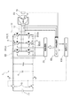
前記インバータ回路を構成する複数のスイッチング素子のそれぞれに駆動信号を伝達して、前記スイッチング素子をオフ状態からオン状態に遷移させるターンオンと、前記スイッチング素子をオン状態からオフ状態に遷移させるターンオフとを、前記スイッチング素子に行わせる駆動回路と、
前記スイッチング素子のそれぞれに流れる電流を検出する電流検出回路と、を備え、
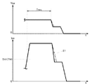
前記駆動回路は、前記電流検出回路により検出された電流が予め規定された過電流しきい値以上の場合に、遅延抵抗を介して前記駆動信号を伝達して、前記スイッチング素子をターンオフさせるソフトターンオフ回路を備え、
前記ソフトターンオフ回路は、前記遅延抵抗に並列接続されたコンデンサを備える。
以下、上記において説明したインバータ装置(1)の概要について簡単に説明する。
前記インバータ回路(10)を構成する複数のスイッチング素子(3)のそれぞれに駆動信号を伝達して、前記スイッチング素子(3)をオフ状態からオン状態に遷移させるターンオンと、前記スイッチング素子(3)をオン状態からオフ状態に遷移させるターンオフとを、前記スイッチング素子(3)に行わせる駆動回路(20)と、
前記スイッチング素子(3)のそれぞれに流れる電流を検出する電流検出回路(26)と、を備え、
前記駆動回路(20)は、前記電流検出回路(26)により検出された電流が予め規定された過電流しきい値(TH)以上の場合に、遅延抵抗(Rs)を介して前記駆動信号を伝達して、前記スイッチング素子(3)をターンオフさせるソフトターンオフ回路(23)を備え、
前記ソフトターンオフ回路(23)は、前記遅延抵抗(Rs)に並列接続されたコンデンサ(Cs)を備える。
Cs ≦ (Qg/2)/Vge
を満たすように設定されている。
3 :スイッチング素子
10 :インバータ回路
11 :高圧バッテリ(直流電源)
20 :駆動回路
23 :ソフトターンオフ回路
30 :アーム
31 :上段側スイッチング素子
32 :下段側スイッチング素子
80 :回転電機
Cs :コンデンサ
G :ゲート端子
Qg :充電電荷量
Rc :シャント抵抗(電流検出回路)
Rr :制限抵抗(抵抗器)
Rs :遅延抵抗
TH :過電流しきい値
TH1 :第1過電流しきい値(過電流しきい値)
TH2 :第2過電流しきい値(過電流しきい値)
Vge :ゲート電圧(制御端子電圧)
ref :基準電圧(過電流しきい値)
Claims (4)
- 直流電力と複数相の交流電力との間で電力を変換するインバータ回路を備えたインバータ装置であって、
前記インバータ回路を構成する複数のスイッチング素子のそれぞれに駆動信号を伝達して、前記スイッチング素子をオフ状態からオン状態に遷移させるターンオンと、前記スイッチング素子をオン状態からオフ状態に遷移させるターンオフとを、前記スイッチング素子に行わせる駆動回路と、
前記スイッチング素子のそれぞれに流れる電流を検出する電流検出回路と、を備え、
前記駆動回路は、前記電流検出回路により検出された電流が予め規定された過電流しきい値以上の場合に、遅延抵抗を介して前記駆動信号を伝達して、前記スイッチング素子をターンオフさせるソフトターンオフ回路を備え、
前記ソフトターンオフ回路は、前記遅延抵抗に並列接続されたコンデンサを備え、
前記インバータ回路は、交流の回転電機及び直流電源に接続されて、複数相の交流と直流との間で電力を変換するものであって、上段側スイッチング素子と下段側スイッチング素子との直列回路により構成された交流1相分のアームを複数本備え、
前記過電流しきい値は、複数相全ての前記アームの前記上段側スイッチング素子がオン状態に制御された状態、及び、複数相全ての前記アームの前記下段側スイッチング素子がオン状態に制御された状態の何れかの状態であるアクティブショートサーキット状態において、オン状態に制御された前記スイッチング素子を流れる電流に応じて設定されているインバータ装置。 - 前記コンデンサの容量は、前記スイッチング素子をターンオンさせる際の制御端子の充電電荷量をQg、前記スイッチング素子をターンオンさせる際に制御端子に印加される制御端子電圧をVge、前記コンデンサの容量をCsとして、
Cs ≦ (Qg/2)/Vgeを満たすように設定されている請求項1に記載のインバータ装置。 - 前記ソフトターンオフ回路は、前記遅延抵抗よりも抵抗値が小さく、前記コンデンサに直列接続される抵抗器を備える請求項1又は2に記載のインバータ装置。
- 直流電力と複数相の交流電力との間で電力を変換するインバータ回路を備えたインバータ装置であって、
前記インバータ回路を構成する複数のスイッチング素子のそれぞれに駆動信号を伝達して、前記スイッチング素子をオフ状態からオン状態に遷移させるターンオンと、前記スイッチング素子をオン状態からオフ状態に遷移させるターンオフとを、前記スイッチング素子に行わせる駆動回路と、
前記スイッチング素子のそれぞれに流れる電流を検出する電流検出回路と、を備え、
前記駆動回路は、前記電流検出回路により検出された電流が予め規定された過電流しきい値以上の場合に、遅延抵抗を介して前記駆動信号を伝達して、前記スイッチング素子をターンオフさせるソフトターンオフ回路を備え、
前記ソフトターンオフ回路は、前記遅延抵抗に並列接続されたコンデンサと、前記遅延抵抗よりも抵抗値が小さく、前記コンデンサに直列接続される抵抗器とを備えるインバータ装置。
Priority Applications (5)
| Application Number | Priority Date | Filing Date | Title |
|---|---|---|---|
| JP2016058909A JP6740657B2 (ja) | 2016-03-23 | 2016-03-23 | インバータ装置 |
| US16/078,943 US10622933B2 (en) | 2016-03-23 | 2017-03-03 | Inverter device that reduces a loss caused by switching elements |
| DE112017000287.7T DE112017000287B4 (de) | 2016-03-23 | 2017-03-03 | Invertervorrichtung |
| CN201780015414.3A CN109104886B (zh) | 2016-03-23 | 2017-03-03 | 逆变器装置 |
| PCT/JP2017/008510 WO2017163820A1 (ja) | 2016-03-23 | 2017-03-03 | インバータ装置 |
Applications Claiming Priority (1)
| Application Number | Priority Date | Filing Date | Title |
|---|---|---|---|
| JP2016058909A JP6740657B2 (ja) | 2016-03-23 | 2016-03-23 | インバータ装置 |
Publications (2)
| Publication Number | Publication Date |
|---|---|
| JP2017175771A JP2017175771A (ja) | 2017-09-28 |
| JP6740657B2 true JP6740657B2 (ja) | 2020-08-19 |
Family
ID=59901243
Family Applications (1)
| Application Number | Title | Priority Date | Filing Date |
|---|---|---|---|
| JP2016058909A Active JP6740657B2 (ja) | 2016-03-23 | 2016-03-23 | インバータ装置 |
Country Status (5)
| Country | Link |
|---|---|
| US (1) | US10622933B2 (ja) |
| JP (1) | JP6740657B2 (ja) |
| CN (1) | CN109104886B (ja) |
| DE (1) | DE112017000287B4 (ja) |
| WO (1) | WO2017163820A1 (ja) |
Families Citing this family (10)
| Publication number | Priority date | Publication date | Assignee | Title |
|---|---|---|---|---|
| US10277268B2 (en) * | 2017-06-02 | 2019-04-30 | Psemi Corporation | Method and apparatus for switching of shunt and through switches of a transceiver |
| JP6992696B2 (ja) | 2018-07-26 | 2022-01-13 | オムロン株式会社 | スイッチ回路及び電力変換装置 |
| JP6836207B2 (ja) * | 2018-08-06 | 2021-02-24 | 株式会社デンソー | 駆動回路 |
| JP7052757B2 (ja) * | 2019-03-01 | 2022-04-12 | 株式会社デンソー | スイッチの駆動装置 |
| JP7293738B2 (ja) * | 2019-03-11 | 2023-06-20 | 株式会社豊田自動織機 | 半導体駆動装置 |
| JP7140045B2 (ja) * | 2019-05-15 | 2022-09-21 | 株式会社デンソー | 駆動回路 |
| JP7540291B2 (ja) * | 2020-10-21 | 2024-08-27 | 富士電機株式会社 | パワースイッチング素子の駆動装置 |
| US11811329B2 (en) * | 2021-02-25 | 2023-11-07 | Viswa Nath Sharma | Remotely programmable multi mode bidirectional power converter |
| EP4075652B1 (en) * | 2021-04-14 | 2024-07-31 | Hitachi Energy Ltd | Inverter circuit for an electrical ac motor, electrical drive and method for controlling an electrical drive |
| CN112994502B (zh) * | 2021-04-29 | 2022-09-27 | 东风汽车集团股份有限公司 | 一种车用igbt模组损耗降低电路、控制方法及电机控制器 |
Family Cites Families (10)
| Publication number | Priority date | Publication date | Assignee | Title |
|---|---|---|---|---|
| JP2664735B2 (ja) * | 1988-08-26 | 1997-10-22 | 株式会社東芝 | 高周波加熱装置 |
| US7863865B2 (en) * | 2007-07-26 | 2011-01-04 | Summit Microelectronics, Inc. | Systems and methods for pulse charging a battery |
| JP5562702B2 (ja) * | 2010-03-31 | 2014-07-30 | 株式会社デンソー | 電力変換システムの放電制御装置 |
| JP5533689B2 (ja) * | 2011-01-18 | 2014-06-25 | 株式会社デンソー | 過電流保護装置 |
| JP2014075694A (ja) * | 2012-10-04 | 2014-04-24 | Renesas Electronics Corp | ゲートドライバ、及びスイッチング方法 |
| JP2014117112A (ja) * | 2012-12-12 | 2014-06-26 | Hitachi Power Semiconductor Device Ltd | 半導体制御装置及び電力変換装置 |
| DE102013226564A1 (de) * | 2013-12-19 | 2015-06-25 | Robert Bosch Gmbh | Vorrichtung und Verfahren zum Betreiben einer elektrischen Maschine |
| US9209618B2 (en) * | 2014-05-08 | 2015-12-08 | General Electric Company | Gate drive unit and method for short circuit protection for a power switch |
| JP6237699B2 (ja) * | 2015-05-25 | 2017-11-29 | トヨタ自動車株式会社 | 異常検出装置 |
| JP6613899B2 (ja) * | 2016-01-05 | 2019-12-04 | 富士電機株式会社 | 半導体素子の駆動装置 |
-
2016
- 2016-03-23 JP JP2016058909A patent/JP6740657B2/ja active Active
-
2017
- 2017-03-03 WO PCT/JP2017/008510 patent/WO2017163820A1/ja not_active Ceased
- 2017-03-03 US US16/078,943 patent/US10622933B2/en active Active
- 2017-03-03 DE DE112017000287.7T patent/DE112017000287B4/de active Active
- 2017-03-03 CN CN201780015414.3A patent/CN109104886B/zh active Active
Also Published As
| Publication number | Publication date |
|---|---|
| US10622933B2 (en) | 2020-04-14 |
| CN109104886B (zh) | 2020-11-03 |
| DE112017000287B4 (de) | 2024-11-21 |
| JP2017175771A (ja) | 2017-09-28 |
| DE112017000287T5 (de) | 2018-09-20 |
| WO2017163820A1 (ja) | 2017-09-28 |
| CN109104886A (zh) | 2018-12-28 |
| US20190058388A1 (en) | 2019-02-21 |
Similar Documents
| Publication | Publication Date | Title |
|---|---|---|
| JP6740657B2 (ja) | インバータ装置 | |
| US9853591B2 (en) | Inverter control device | |
| CN101371431B (zh) | 在干扰情况下关断电机的方法和装置 | |
| JP6418252B2 (ja) | 回転電機制御装置 | |
| KR102087573B1 (ko) | 인버터용 작동 상태 회로, 및 인버터의 작동 상태 설정 방법 | |
| CN110383677B (zh) | 电动机的驱动装置以及制冷循环适用设备 | |
| JP6287661B2 (ja) | 回転電機制御装置 | |
| JP6253850B2 (ja) | 交流回転電機の制御装置 | |
| US20190097561A1 (en) | Inverter driver | |
| WO2021090679A1 (ja) | 電力変換装置 | |
| JP7790585B2 (ja) | 電力変換装置、プログラム及び制御方法 | |
| JP7244075B2 (ja) | 充電システム | |
| JP6307983B2 (ja) | インバータ制御装置 | |
| US11728802B2 (en) | Drive circuit | |
| CN106655861A (zh) | 用于电机的逆变器、用于机动车的电驱动装置以及用于运行逆变器的方法 | |
| JP6289597B1 (ja) | 車両用電源装置および車両用電源装置の制御方法 | |
| JP2013511247A (ja) | インバータ | |
| JP7544025B2 (ja) | スイッチの駆動装置 | |
| JP6638504B2 (ja) | インバータ駆動装置 | |
| CN118946471A (zh) | 在故障情况中用交替的空转状态和短路状态对车辆驱动器进行基于迟滞的操控 | |
| CN117044093A (zh) | 冲击电流抑制电路、转换系统以及电动机驱动装置 | |
| JP2018057225A (ja) | インバータ装置 | |
| JP2024043960A (ja) | 昇温装置、及びプログラム | |
| WO2024214506A1 (ja) | 絶縁型電源装置、電源システム、及び電源制御プログラム | |
| JP2022079389A (ja) | 電力変換装置 |
Legal Events
| Date | Code | Title | Description |
|---|---|---|---|
| A621 | Written request for application examination |
Free format text: JAPANESE INTERMEDIATE CODE: A621 Effective date: 20180912 |
|
| A131 | Notification of reasons for refusal |
Free format text: JAPANESE INTERMEDIATE CODE: A131 Effective date: 20191203 |
|
| A521 | Request for written amendment filed |
Free format text: JAPANESE INTERMEDIATE CODE: A523 Effective date: 20200130 |
|
| TRDD | Decision of grant or rejection written | ||
| A01 | Written decision to grant a patent or to grant a registration (utility model) |
Free format text: JAPANESE INTERMEDIATE CODE: A01 Effective date: 20200623 |
|
| A61 | First payment of annual fees (during grant procedure) |
Free format text: JAPANESE INTERMEDIATE CODE: A61 Effective date: 20200706 |
|
| R150 | Certificate of patent or registration of utility model |
Ref document number: 6740657 Country of ref document: JP Free format text: JAPANESE INTERMEDIATE CODE: R150 |