JP6777148B2 - 半導体装置 - Google Patents
半導体装置 Download PDFInfo
- Publication number
- JP6777148B2 JP6777148B2 JP2018530284A JP2018530284A JP6777148B2 JP 6777148 B2 JP6777148 B2 JP 6777148B2 JP 2018530284 A JP2018530284 A JP 2018530284A JP 2018530284 A JP2018530284 A JP 2018530284A JP 6777148 B2 JP6777148 B2 JP 6777148B2
- Authority
- JP
- Japan
- Prior art keywords
- solder
- intermediate plate
- semiconductor device
- semiconductor chip
- electrode substrate
- Prior art date
- Legal status (The legal status is an assumption and is not a legal conclusion. Google has not performed a legal analysis and makes no representation as to the accuracy of the status listed.)
- Active
Links
Images



Classifications
-
- H—ELECTRICITY
- H10—SEMICONDUCTOR DEVICES; ELECTRIC SOLID-STATE DEVICES NOT OTHERWISE PROVIDED FOR
- H10W—GENERIC PACKAGES, INTERCONNECTIONS, CONNECTORS OR OTHER CONSTRUCTIONAL DETAILS OF DEVICES COVERED BY CLASS H10
- H10W72/00—Interconnections or connectors in packages
- H10W72/071—Connecting or disconnecting
- H10W72/076—Connecting or disconnecting of strap connectors
-
- H—ELECTRICITY
- H10—SEMICONDUCTOR DEVICES; ELECTRIC SOLID-STATE DEVICES NOT OTHERWISE PROVIDED FOR
- H10W—GENERIC PACKAGES, INTERCONNECTIONS, CONNECTORS OR OTHER CONSTRUCTIONAL DETAILS OF DEVICES COVERED BY CLASS H10
- H10W72/00—Interconnections or connectors in packages
-
- H—ELECTRICITY
- H10—SEMICONDUCTOR DEVICES; ELECTRIC SOLID-STATE DEVICES NOT OTHERWISE PROVIDED FOR
- H10W—GENERIC PACKAGES, INTERCONNECTIONS, CONNECTORS OR OTHER CONSTRUCTIONAL DETAILS OF DEVICES COVERED BY CLASS H10
- H10W72/00—Interconnections or connectors in packages
- H10W72/071—Connecting or disconnecting
-
- H—ELECTRICITY
- H10—SEMICONDUCTOR DEVICES; ELECTRIC SOLID-STATE DEVICES NOT OTHERWISE PROVIDED FOR
- H10W—GENERIC PACKAGES, INTERCONNECTIONS, CONNECTORS OR OTHER CONSTRUCTIONAL DETAILS OF DEVICES COVERED BY CLASS H10
- H10W72/00—Interconnections or connectors in packages
- H10W72/071—Connecting or disconnecting
- H10W72/073—Connecting or disconnecting of die-attach connectors
- H10W72/07302—Connecting or disconnecting of die-attach connectors using an auxiliary member
-
- H—ELECTRICITY
- H10—SEMICONDUCTOR DEVICES; ELECTRIC SOLID-STATE DEVICES NOT OTHERWISE PROVIDED FOR
- H10W—GENERIC PACKAGES, INTERCONNECTIONS, CONNECTORS OR OTHER CONSTRUCTIONAL DETAILS OF DEVICES COVERED BY CLASS H10
- H10W72/00—Interconnections or connectors in packages
- H10W72/071—Connecting or disconnecting
- H10W72/073—Connecting or disconnecting of die-attach connectors
- H10W72/07331—Connecting techniques
- H10W72/07336—Soldering or alloying
-
- H—ELECTRICITY
- H10—SEMICONDUCTOR DEVICES; ELECTRIC SOLID-STATE DEVICES NOT OTHERWISE PROVIDED FOR
- H10W—GENERIC PACKAGES, INTERCONNECTIONS, CONNECTORS OR OTHER CONSTRUCTIONAL DETAILS OF DEVICES COVERED BY CLASS H10
- H10W72/00—Interconnections or connectors in packages
- H10W72/071—Connecting or disconnecting
- H10W72/073—Connecting or disconnecting of die-attach connectors
- H10W72/07341—Controlling the bonding environment, e.g. atmosphere composition or temperature
-
- H—ELECTRICITY
- H10—SEMICONDUCTOR DEVICES; ELECTRIC SOLID-STATE DEVICES NOT OTHERWISE PROVIDED FOR
- H10W—GENERIC PACKAGES, INTERCONNECTIONS, CONNECTORS OR OTHER CONSTRUCTIONAL DETAILS OF DEVICES COVERED BY CLASS H10
- H10W72/00—Interconnections or connectors in packages
- H10W72/071—Connecting or disconnecting
- H10W72/073—Connecting or disconnecting of die-attach connectors
- H10W72/07351—Connecting or disconnecting of die-attach connectors characterised by changes in properties of the die-attach connectors during connecting
- H10W72/07354—Connecting or disconnecting of die-attach connectors characterised by changes in properties of the die-attach connectors during connecting changes in dispositions
-
- H—ELECTRICITY
- H10—SEMICONDUCTOR DEVICES; ELECTRIC SOLID-STATE DEVICES NOT OTHERWISE PROVIDED FOR
- H10W—GENERIC PACKAGES, INTERCONNECTIONS, CONNECTORS OR OTHER CONSTRUCTIONAL DETAILS OF DEVICES COVERED BY CLASS H10
- H10W72/00—Interconnections or connectors in packages
- H10W72/071—Connecting or disconnecting
- H10W72/076—Connecting or disconnecting of strap connectors
- H10W72/07631—Techniques
- H10W72/07636—Soldering or alloying
-
- H—ELECTRICITY
- H10—SEMICONDUCTOR DEVICES; ELECTRIC SOLID-STATE DEVICES NOT OTHERWISE PROVIDED FOR
- H10W—GENERIC PACKAGES, INTERCONNECTIONS, CONNECTORS OR OTHER CONSTRUCTIONAL DETAILS OF DEVICES COVERED BY CLASS H10
- H10W72/00—Interconnections or connectors in packages
- H10W72/30—Die-attach connectors
- H10W72/341—Dispositions of die-attach connectors, e.g. layouts
- H10W72/347—Dispositions of multiple die-attach connectors
-
- H—ELECTRICITY
- H10—SEMICONDUCTOR DEVICES; ELECTRIC SOLID-STATE DEVICES NOT OTHERWISE PROVIDED FOR
- H10W—GENERIC PACKAGES, INTERCONNECTIONS, CONNECTORS OR OTHER CONSTRUCTIONAL DETAILS OF DEVICES COVERED BY CLASS H10
- H10W72/00—Interconnections or connectors in packages
- H10W72/30—Die-attach connectors
- H10W72/351—Materials of die-attach connectors
- H10W72/352—Materials of die-attach connectors comprising metals or metalloids, e.g. solders
-
- H—ELECTRICITY
- H10—SEMICONDUCTOR DEVICES; ELECTRIC SOLID-STATE DEVICES NOT OTHERWISE PROVIDED FOR
- H10W—GENERIC PACKAGES, INTERCONNECTIONS, CONNECTORS OR OTHER CONSTRUCTIONAL DETAILS OF DEVICES COVERED BY CLASS H10
- H10W72/00—Interconnections or connectors in packages
- H10W72/30—Die-attach connectors
- H10W72/381—Auxiliary members
- H10W72/383—Reinforcing structures, e.g. collars
-
- H—ELECTRICITY
- H10—SEMICONDUCTOR DEVICES; ELECTRIC SOLID-STATE DEVICES NOT OTHERWISE PROVIDED FOR
- H10W—GENERIC PACKAGES, INTERCONNECTIONS, CONNECTORS OR OTHER CONSTRUCTIONAL DETAILS OF DEVICES COVERED BY CLASS H10
- H10W72/00—Interconnections or connectors in packages
- H10W72/60—Strap connectors, e.g. thick copper clips for grounding of power devices
- H10W72/651—Materials of strap connectors
- H10W72/652—Materials of strap connectors comprising metals or metalloids, e.g. silver
-
- H—ELECTRICITY
- H10—SEMICONDUCTOR DEVICES; ELECTRIC SOLID-STATE DEVICES NOT OTHERWISE PROVIDED FOR
- H10W—GENERIC PACKAGES, INTERCONNECTIONS, CONNECTORS OR OTHER CONSTRUCTIONAL DETAILS OF DEVICES COVERED BY CLASS H10
- H10W72/00—Interconnections or connectors in packages
- H10W72/851—Dispositions of multiple connectors or interconnections
- H10W72/874—On different surfaces
- H10W72/884—Die-attach connectors and bond wires
-
- H—ELECTRICITY
- H10—SEMICONDUCTOR DEVICES; ELECTRIC SOLID-STATE DEVICES NOT OTHERWISE PROVIDED FOR
- H10W—GENERIC PACKAGES, INTERCONNECTIONS, CONNECTORS OR OTHER CONSTRUCTIONAL DETAILS OF DEVICES COVERED BY CLASS H10
- H10W74/00—Encapsulations, e.g. protective coatings
-
- H—ELECTRICITY
- H10—SEMICONDUCTOR DEVICES; ELECTRIC SOLID-STATE DEVICES NOT OTHERWISE PROVIDED FOR
- H10W—GENERIC PACKAGES, INTERCONNECTIONS, CONNECTORS OR OTHER CONSTRUCTIONAL DETAILS OF DEVICES COVERED BY CLASS H10
- H10W90/00—Package configurations
- H10W90/701—Package configurations characterised by the relative positions of pads or connectors relative to package parts
- H10W90/731—Package configurations characterised by the relative positions of pads or connectors relative to package parts of die-attach connectors
- H10W90/736—Package configurations characterised by the relative positions of pads or connectors relative to package parts of die-attach connectors between a chip and a stacked lead frame, conducting package substrate or heat sink
-
- H—ELECTRICITY
- H10—SEMICONDUCTOR DEVICES; ELECTRIC SOLID-STATE DEVICES NOT OTHERWISE PROVIDED FOR
- H10W—GENERIC PACKAGES, INTERCONNECTIONS, CONNECTORS OR OTHER CONSTRUCTIONAL DETAILS OF DEVICES COVERED BY CLASS H10
- H10W90/00—Package configurations
- H10W90/701—Package configurations characterised by the relative positions of pads or connectors relative to package parts
- H10W90/761—Package configurations characterised by the relative positions of pads or connectors relative to package parts of strap connectors
- H10W90/766—Package configurations characterised by the relative positions of pads or connectors relative to package parts of strap connectors between a chip and a stacked lead frame, conducting package substrate or heat sink
Landscapes
- Cooling Or The Like Of Semiconductors Or Solid State Devices (AREA)
- Die Bonding (AREA)
Description
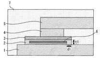
図1は、実施の形態1に係る半導体装置を示す断面図である。本実施の形態に係る半導体装置は、例えば自動車動力用モータを駆動する電源に用いられる。電極基板1の上面に第1のはんだ2を介して半導体チップ3が接合されている。半導体チップ3の上面に第2のはんだ4を介してリードフレーム5が接合されている。
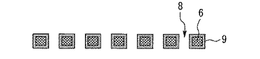
図3は、実施の形態2に係る中間板を示す平面図である。図4は、図3のI−IIに沿った断面図である。本実施の形態は、中間板6の構成以外は実施の形態1と同様である。
図5は、実施の形態3に係る半導体装置を示す断面図である。電極基板1と半導体チップ3の端部との間に、アルミワイヤなどにより複数のバンプ10が設けられている。バンプによって半導体チップ3と電極基板1との距離を確保することができるため、半導体チップ3が傾いて実装されて第1のはんだ2が部分的に薄くなるのを防ぐことができる。
Claims (17)
- 電極基板と、
前記電極基板の上面に第1のはんだを介して接合された半導体チップと、
前記半導体チップの上面に第2のはんだを介して接合されたリードフレームと、
前記電極基板と前記半導体チップとの間において前記第1のはんだ中に設けられた中間板と、
前記電極基板と前記半導体チップとの間に設けられた複数のバンプとを備え、
前記中間板の耐力は、半導体装置の使用温度範囲の全てにおいて前記電極基板及び前記第1のはんだの耐力よりも大きく、
前記中間板は、平面視において前記複数のバンプの内側に配置されていることを特徴とする半導体装置。 - 前記中間板の厚みは前記複数のバンプの高さより薄いことを特徴とする請求項1に記載の半導体装置。
- 電極基板と、
前記電極基板の上面に第1のはんだを介して接合された半導体チップと、
前記半導体チップの上面に第2のはんだを介して接合されたリードフレームと、
前記電極基板と前記半導体チップとの間において前記第1のはんだ中に設けられた中間板とを備え、
前記中間板の耐力は、半導体装置の使用温度範囲の全てにおいて前記電極基板及び前記第1のはんだの耐力よりも大きく、
前記中間板の主な材料は銅であることを特徴とする半導体装置。 - 前記使用温度範囲は−55℃から200℃であることを特徴とする請求項1〜3の何れか1項に記載の半導体装置。
- 前記中間板は、平面視において前記半導体チップ及び前記第1のはんだの内側に配置されていることを特徴とする請求項1〜4の何れか1項に記載の半導体装置。
- 前記半導体チップの端部と前記中間板の端部との間隔は、前記第1のはんだの厚みより大きいことを特徴とする請求項5に記載の半導体装置。
- 前記第2のはんだは、平面視において前記中間板の内側に配置されていることを特徴とする請求項1〜6の何れか1項に記載の半導体装置。
- 前記中間板の表面を覆い、前記中間板よりも前記第1のはんだに対する濡れ性が高いめっき膜を更に備えることを特徴とする請求項1〜7の何れか1項に記載の半導体装置。
- 前記めっき膜の主な材料はニッケルであることを特徴とする請求項8に記載の半導体装置。
- 前記中間板に複数の貫通孔が設けられていることを特徴とする請求項1〜9の何れか1項に記載の半導体装置。
- 前記中間板に複数の貫通孔が設けられ、
前記めっき膜は前記複数の貫通孔の側壁にも形成されていることを特徴とする請求項8又は9に記載の半導体装置。 - 前記貫通孔の大きさは500μmΦ以下であることを特徴とする請求項10又は11に記載の半導体装置。
- 前記電極基板の主な材料はアルミであることを特徴とする請求項1〜12の何れか1項に記載の半導体装置。
- 前記中間板の主な材料はモリブデンであることを特徴とする請求項1又は2に記載の半導体装置。
- 前記半導体チップは化合物半導体を用いていることを特徴とする請求項1〜14の何れか1項に記載の半導体装置。
- 前記化合物半導体の主な材料はカーボンを有することを特徴とする請求項15に記載の半導体装置。
- 自動車動力用モータを駆動する電源に用いられることを特徴とする請求項1〜16の何れか1項に記載の半導体装置。
Applications Claiming Priority (1)
| Application Number | Priority Date | Filing Date | Title |
|---|---|---|---|
| PCT/JP2016/072158 WO2018020640A1 (ja) | 2016-07-28 | 2016-07-28 | 半導体装置 |
Publications (2)
| Publication Number | Publication Date |
|---|---|
| JPWO2018020640A1 JPWO2018020640A1 (ja) | 2018-12-13 |
| JP6777148B2 true JP6777148B2 (ja) | 2020-10-28 |
Family
ID=61016579
Family Applications (1)
| Application Number | Title | Priority Date | Filing Date |
|---|---|---|---|
| JP2018530284A Active JP6777148B2 (ja) | 2016-07-28 | 2016-07-28 | 半導体装置 |
Country Status (5)
| Country | Link |
|---|---|
| US (1) | US12009332B2 (ja) |
| JP (1) | JP6777148B2 (ja) |
| CN (1) | CN109478543B (ja) |
| DE (1) | DE112016007096B4 (ja) |
| WO (1) | WO2018020640A1 (ja) |
Families Citing this family (5)
| Publication number | Priority date | Publication date | Assignee | Title |
|---|---|---|---|---|
| WO2020213167A1 (ja) * | 2019-04-19 | 2020-10-22 | 三菱電機株式会社 | 半導体装置およびその製造方法 |
| CN114423557A (zh) * | 2019-10-23 | 2022-04-29 | 阿尔法装配解决方案公司 | 用于电子组件的工程化材料 |
| JP7543655B2 (ja) * | 2020-02-14 | 2024-09-03 | 富士電機株式会社 | 半導体モジュール |
| CN114743947B (zh) * | 2022-04-11 | 2023-09-19 | 中国工程物理研究院电子工程研究所 | 基于to形式的功率器件封装结构及封装方法 |
| CN121942350A (zh) * | 2023-09-28 | 2026-04-28 | 古河电气工业株式会社 | 接合用膜、半导体模块、逆变器、电子设备以及半导体模块的制造方法 |
Family Cites Families (41)
| Publication number | Priority date | Publication date | Assignee | Title |
|---|---|---|---|---|
| JPS5665650U (ja) * | 1979-10-23 | 1981-06-01 | ||
| JPS56172938U (ja) * | 1980-05-23 | 1981-12-21 | ||
| DE3685647T2 (de) * | 1985-07-16 | 1993-01-07 | Nippon Telegraph & Telephone | Verbindungskontakte zwischen substraten und verfahren zur herstellung derselben. |
| JPS63251127A (ja) * | 1987-04-06 | 1988-10-18 | Ngk Insulators Ltd | セラミック製部材と金属製部材の結合方法 |
| US5188280A (en) * | 1989-04-28 | 1993-02-23 | Hitachi Ltd. | Method of bonding metals, and method and apparatus for producing semiconductor integrated circuit device using said method of bonding metals |
| EP0568313A2 (en) * | 1992-05-01 | 1993-11-03 | Nippon CMK Corp. | A method of manufacturing a multilayer printed wiring board |
| JP2989406B2 (ja) * | 1993-01-29 | 1999-12-13 | シャープ株式会社 | 半導体装置用プリプレーテッドフレーム及びその製造方法 |
| US6070321A (en) * | 1997-07-09 | 2000-06-06 | International Business Machines Corporation | Solder disc connection |
| US6158644A (en) * | 1998-04-30 | 2000-12-12 | International Business Machines Corporation | Method for enhancing fatigue life of ball grid arrays |
| JP2000332369A (ja) * | 1999-05-25 | 2000-11-30 | Mitsui Mining & Smelting Co Ltd | プリント回路板及びその製造方法 |
| US6197618B1 (en) * | 2000-05-04 | 2001-03-06 | General Semiconductor Ireland | Semiconductor device fabrication using adhesives |
| CN1259200C (zh) * | 2000-10-02 | 2006-06-14 | 松下电器产业株式会社 | 卡型记录媒体及其制造方法 |
| JP2002203942A (ja) * | 2000-12-28 | 2002-07-19 | Fuji Electric Co Ltd | パワー半導体モジュール |
| US20040078964A1 (en) * | 2001-03-07 | 2004-04-29 | Kazuhiro Itou | Land portion of printed wiring board, method for manufacturing printed wiring board, and printed wiring board mounting method |
| JP4848539B2 (ja) * | 2001-08-23 | 2011-12-28 | Dowaメタルテック株式会社 | 放熱板およびパワー半導体モジュール、icパッケージ |
| US6821667B2 (en) * | 2001-10-01 | 2004-11-23 | Delphi Technologies, Inc. | Fuel cell stack having foil interconnects and laminated spacers |
| JP2003133337A (ja) | 2001-10-23 | 2003-05-09 | Nissan Motor Co Ltd | 半導体実装構造および半導体実装方法 |
| US7532481B2 (en) * | 2004-04-05 | 2009-05-12 | Mitsubishi Materials Corporation | Al/AlN joint material, base plate for power module, power module, and manufacturing method of Al/AlN joint material |
| JP5491682B2 (ja) * | 2004-08-13 | 2014-05-14 | 日立金属株式会社 | 太陽電池用平角導体及びその製造方法並びに太陽電池用リード線 |
| JP4343117B2 (ja) * | 2005-01-07 | 2009-10-14 | 株式会社ルネサステクノロジ | 半導体装置およびその製造方法 |
| JP4421528B2 (ja) * | 2005-07-28 | 2010-02-24 | シャープ株式会社 | 半田付け実装構造およびその製造方法、並びにその利用 |
| JP4569423B2 (ja) * | 2005-08-31 | 2010-10-27 | 株式会社日立製作所 | 半導体装置の製造方法 |
| JP2007157863A (ja) * | 2005-12-02 | 2007-06-21 | Hitachi Ltd | パワー半導体装置及びその製造方法 |
| US20090186195A1 (en) * | 2006-09-08 | 2009-07-23 | Reactive Nanotechnologies, Inc. | Reactive Multilayer Joining With Improved Metallization Techniques |
| JP2008098607A (ja) * | 2006-09-13 | 2008-04-24 | Hitachi Cable Ltd | 太陽電池用接続リード線及びその製造方法並びに太陽電池 |
| JP5272191B2 (ja) * | 2007-08-31 | 2013-08-28 | 三菱電機株式会社 | 半導体装置および半導体装置の製造方法 |
| JP2009224560A (ja) * | 2008-03-17 | 2009-10-01 | Denso Corp | 半導体装置およびその製造方法 |
| JP5241344B2 (ja) * | 2008-06-30 | 2013-07-17 | 日立オートモティブシステムズ株式会社 | パワーモジュール及び電力変換装置 |
| WO2012073306A1 (ja) | 2010-11-29 | 2012-06-07 | トヨタ自動車株式会社 | パワーモジュール |
| JP5325917B2 (ja) * | 2011-03-17 | 2013-10-23 | 株式会社東芝 | 半導体装置及びその製造方法 |
| JP2013113638A (ja) | 2011-11-25 | 2013-06-10 | Toyota Motor Corp | 半導体装置 |
| KR102007780B1 (ko) * | 2012-07-31 | 2019-10-21 | 삼성전자주식회사 | 멀티 범프 구조의 전기적 연결부를 포함하는 반도체 소자의 제조방법 |
| JP2014041876A (ja) * | 2012-08-21 | 2014-03-06 | Mitsubishi Electric Corp | 電力用半導体装置 |
| JP5686128B2 (ja) * | 2012-11-29 | 2015-03-18 | トヨタ自動車株式会社 | 半導体装置 |
| US8896118B2 (en) * | 2013-03-13 | 2014-11-25 | Texas Instruments Incorporated | Electronic assembly with copper pillar attach substrate |
| JP6020731B2 (ja) * | 2013-08-29 | 2016-11-02 | 三菱電機株式会社 | 半導体モジュール、半導体装置、及び自動車 |
| JP6399738B2 (ja) * | 2013-09-25 | 2018-10-03 | 富士電機株式会社 | 半導体装置 |
| JP2016046403A (ja) * | 2014-08-25 | 2016-04-04 | トヨタ自動車株式会社 | 半導体装置 |
| CN105575924B (zh) * | 2014-10-15 | 2018-07-03 | 台达电子工业股份有限公司 | 功率模块 |
| US9633957B2 (en) * | 2014-11-28 | 2017-04-25 | Infineon Technologies Ag | Semiconductor device, a power semiconductor device, and a method for processing a semiconductor device |
| KR102430984B1 (ko) * | 2015-09-22 | 2022-08-09 | 삼성전자주식회사 | 반도체 장치 및 이의 제조 방법 |
-
2016
- 2016-07-28 WO PCT/JP2016/072158 patent/WO2018020640A1/ja not_active Ceased
- 2016-07-28 CN CN201680087903.5A patent/CN109478543B/zh active Active
- 2016-07-28 US US16/088,455 patent/US12009332B2/en active Active
- 2016-07-28 JP JP2018530284A patent/JP6777148B2/ja active Active
- 2016-07-28 DE DE112016007096.9T patent/DE112016007096B4/de active Active
Also Published As
| Publication number | Publication date |
|---|---|
| WO2018020640A1 (ja) | 2018-02-01 |
| US12009332B2 (en) | 2024-06-11 |
| DE112016007096B4 (de) | 2023-06-29 |
| DE112016007096T5 (de) | 2019-04-18 |
| US20190157235A1 (en) | 2019-05-23 |
| CN109478543A (zh) | 2019-03-15 |
| JPWO2018020640A1 (ja) | 2018-12-13 |
| CN109478543B (zh) | 2022-07-05 |
Similar Documents
| Publication | Publication Date | Title |
|---|---|---|
| JP6199397B2 (ja) | 半導体装置およびその製造方法 | |
| US10727163B2 (en) | Semiconductor device | |
| JP5572678B2 (ja) | クラッド型ベースプレートを含む半導体装置 | |
| JP4569473B2 (ja) | 樹脂封止型パワー半導体モジュール | |
| JP6945418B2 (ja) | 半導体装置および半導体装置の製造方法 | |
| JP6337957B2 (ja) | 半導体モジュールユニットおよび半導体モジュール | |
| JP6777148B2 (ja) | 半導体装置 | |
| WO2007145303A1 (ja) | 半導体モジュールおよびその製造方法 | |
| US10879209B2 (en) | Encapsulated stress mitigation layer and power electronic assemblies incorporating the same | |
| WO2011040313A1 (ja) | 半導体モジュールおよびその製造方法 | |
| US10283430B2 (en) | Power semiconductor device and method for manufacturing same | |
| CN117438386A (zh) | 半导体装置、半导体装置的制造方法及电力转换装置 | |
| JP5899952B2 (ja) | 半導体モジュール | |
| JP2006190728A (ja) | 電力用半導体装置 | |
| JP2011176087A (ja) | 半導体モジュール、及び電力変換装置 | |
| JP5100674B2 (ja) | インバータ装置 | |
| JP2015002305A (ja) | 半導体装置 | |
| JP2014187180A (ja) | 半導体装置用接合体、パワーモジュール用基板及びパワーモジュール | |
| JP2019040955A (ja) | 半導体モジュールの製造方法 | |
| JP2014120717A (ja) | 電子装置およびその製造方法 | |
| KR102684858B1 (ko) | 열방출 포스트 접합 반도체 패키지 및 이의 제조방법 | |
| Barlow et al. | High-temperature high-power packaging techniques for HEV traction applications | |
| JP2020068331A (ja) | 半導体装置 | |
| JP2023162108A (ja) | 樹脂封止型半導体装置及び電力変換装置 | |
| JP2023131815A (ja) | 半導体装置 |
Legal Events
| Date | Code | Title | Description |
|---|---|---|---|
| A621 | Written request for application examination |
Free format text: JAPANESE INTERMEDIATE CODE: A621 Effective date: 20180816 |
|
| A131 | Notification of reasons for refusal |
Free format text: JAPANESE INTERMEDIATE CODE: A131 Effective date: 20191023 |
|
| A521 | Request for written amendment filed |
Free format text: JAPANESE INTERMEDIATE CODE: A523 Effective date: 20191119 |
|
| A131 | Notification of reasons for refusal |
Free format text: JAPANESE INTERMEDIATE CODE: A131 Effective date: 20200526 |
|
| A521 | Request for written amendment filed |
Free format text: JAPANESE INTERMEDIATE CODE: A523 Effective date: 20200617 |
|
| TRDD | Decision of grant or rejection written | ||
| A01 | Written decision to grant a patent or to grant a registration (utility model) |
Free format text: JAPANESE INTERMEDIATE CODE: A01 Effective date: 20200908 |
|
| A61 | First payment of annual fees (during grant procedure) |
Free format text: JAPANESE INTERMEDIATE CODE: A61 Effective date: 20200921 |
|
| R150 | Certificate of patent or registration of utility model |
Ref document number: 6777148 Country of ref document: JP Free format text: JAPANESE INTERMEDIATE CODE: R150 |
|
| R250 | Receipt of annual fees |
Free format text: JAPANESE INTERMEDIATE CODE: R250 |
|
| R250 | Receipt of annual fees |
Free format text: JAPANESE INTERMEDIATE CODE: R250 |
|
| R250 | Receipt of annual fees |
Free format text: JAPANESE INTERMEDIATE CODE: R250 |