JP6797005B2 - 半導体装置 - Google Patents
半導体装置 Download PDFInfo
- Publication number
- JP6797005B2 JP6797005B2 JP2016227933A JP2016227933A JP6797005B2 JP 6797005 B2 JP6797005 B2 JP 6797005B2 JP 2016227933 A JP2016227933 A JP 2016227933A JP 2016227933 A JP2016227933 A JP 2016227933A JP 6797005 B2 JP6797005 B2 JP 6797005B2
- Authority
- JP
- Japan
- Prior art keywords
- region
- semiconductor
- type
- semiconductor device
- trench
- Prior art date
- Legal status (The legal status is an assumption and is not a legal conclusion. Google has not performed a legal analysis and makes no representation as to the accuracy of the status listed.)
- Active
Links
Images











Classifications
-
- H—ELECTRICITY
- H10—SEMICONDUCTOR DEVICES; ELECTRIC SOLID-STATE DEVICES NOT OTHERWISE PROVIDED FOR
- H10D—INORGANIC ELECTRIC SEMICONDUCTOR DEVICES
- H10D62/00—Semiconductor bodies, or regions thereof, of devices having potential barriers
- H10D62/10—Shapes, relative sizes or dispositions of the regions of the semiconductor bodies; Shapes of the semiconductor bodies
- H10D62/124—Shapes, relative sizes or dispositions of the regions of semiconductor bodies or of junctions between the regions
- H10D62/126—Top-view geometrical layouts of the regions or the junctions
- H10D62/127—Top-view geometrical layouts of the regions or the junctions of cellular field-effect devices, e.g. multicellular DMOS transistors or IGBTs
-
- H—ELECTRICITY
- H10—SEMICONDUCTOR DEVICES; ELECTRIC SOLID-STATE DEVICES NOT OTHERWISE PROVIDED FOR
- H10D—INORGANIC ELECTRIC SEMICONDUCTOR DEVICES
- H10D84/00—Integrated devices formed in or on semiconductor substrates that comprise only semiconducting layers, e.g. on Si wafers or on GaAs-on-Si wafers
- H10D84/60—Integrated devices formed in or on semiconductor substrates that comprise only semiconducting layers, e.g. on Si wafers or on GaAs-on-Si wafers characterised by the integration of at least one component covered by groups H10D10/00 or H10D18/00, e.g. integration of BJTs
- H10D84/641—Combinations of only vertical BJTs
-
- H—ELECTRICITY
- H10—SEMICONDUCTOR DEVICES; ELECTRIC SOLID-STATE DEVICES NOT OTHERWISE PROVIDED FOR
- H10D—INORGANIC ELECTRIC SEMICONDUCTOR DEVICES
- H10D12/00—Bipolar devices controlled by the field effect, e.g. insulated-gate bipolar transistors [IGBT]
- H10D12/01—Manufacture or treatment
- H10D12/031—Manufacture or treatment of IGBTs
- H10D12/032—Manufacture or treatment of IGBTs of vertical IGBTs
-
- H—ELECTRICITY
- H10—SEMICONDUCTOR DEVICES; ELECTRIC SOLID-STATE DEVICES NOT OTHERWISE PROVIDED FOR
- H10D—INORGANIC ELECTRIC SEMICONDUCTOR DEVICES
- H10D12/00—Bipolar devices controlled by the field effect, e.g. insulated-gate bipolar transistors [IGBT]
- H10D12/01—Manufacture or treatment
- H10D12/031—Manufacture or treatment of IGBTs
- H10D12/032—Manufacture or treatment of IGBTs of vertical IGBTs
- H10D12/035—Etching a recess in the emitter region
-
- H—ELECTRICITY
- H10—SEMICONDUCTOR DEVICES; ELECTRIC SOLID-STATE DEVICES NOT OTHERWISE PROVIDED FOR
- H10D—INORGANIC ELECTRIC SEMICONDUCTOR DEVICES
- H10D12/00—Bipolar devices controlled by the field effect, e.g. insulated-gate bipolar transistors [IGBT]
- H10D12/01—Manufacture or treatment
- H10D12/031—Manufacture or treatment of IGBTs
- H10D12/032—Manufacture or treatment of IGBTs of vertical IGBTs
- H10D12/038—Manufacture or treatment of IGBTs of vertical IGBTs having a recessed gate, e.g. trench-gate IGBTs
-
- H—ELECTRICITY
- H10—SEMICONDUCTOR DEVICES; ELECTRIC SOLID-STATE DEVICES NOT OTHERWISE PROVIDED FOR
- H10D—INORGANIC ELECTRIC SEMICONDUCTOR DEVICES
- H10D12/00—Bipolar devices controlled by the field effect, e.g. insulated-gate bipolar transistors [IGBT]
- H10D12/411—Insulated-gate bipolar transistors [IGBT]
- H10D12/441—Vertical IGBTs
- H10D12/461—Vertical IGBTs having non-planar surfaces, e.g. having trenches, recesses or pillars in the surfaces of the emitter, base or collector regions
-
- H—ELECTRICITY
- H10—SEMICONDUCTOR DEVICES; ELECTRIC SOLID-STATE DEVICES NOT OTHERWISE PROVIDED FOR
- H10D—INORGANIC ELECTRIC SEMICONDUCTOR DEVICES
- H10D12/00—Bipolar devices controlled by the field effect, e.g. insulated-gate bipolar transistors [IGBT]
- H10D12/411—Insulated-gate bipolar transistors [IGBT]
- H10D12/441—Vertical IGBTs
- H10D12/461—Vertical IGBTs having non-planar surfaces, e.g. having trenches, recesses or pillars in the surfaces of the emitter, base or collector regions
- H10D12/481—Vertical IGBTs having non-planar surfaces, e.g. having trenches, recesses or pillars in the surfaces of the emitter, base or collector regions having gate structures on slanted surfaces, on vertical surfaces, or in grooves, e.g. trench gate IGBTs
-
- H—ELECTRICITY
- H10—SEMICONDUCTOR DEVICES; ELECTRIC SOLID-STATE DEVICES NOT OTHERWISE PROVIDED FOR
- H10D—INORGANIC ELECTRIC SEMICONDUCTOR DEVICES
- H10D62/00—Semiconductor bodies, or regions thereof, of devices having potential barriers
- H10D62/10—Shapes, relative sizes or dispositions of the regions of the semiconductor bodies; Shapes of the semiconductor bodies
- H10D62/102—Constructional design considerations for preventing surface leakage or controlling electric field concentration
- H10D62/103—Constructional design considerations for preventing surface leakage or controlling electric field concentration for increasing or controlling the breakdown voltage of reverse-biased devices
- H10D62/105—Constructional design considerations for preventing surface leakage or controlling electric field concentration for increasing or controlling the breakdown voltage of reverse-biased devices by having particular doping profiles, shapes or arrangements of PN junctions; by having supplementary regions, e.g. junction termination extension [JTE]
- H10D62/106—Constructional design considerations for preventing surface leakage or controlling electric field concentration for increasing or controlling the breakdown voltage of reverse-biased devices by having particular doping profiles, shapes or arrangements of PN junctions; by having supplementary regions, e.g. junction termination extension [JTE] having supplementary regions doped oppositely to or in rectifying contact with regions of the semiconductor bodies, e.g. guard rings with PN or Schottky junctions
-
- H—ELECTRICITY
- H10—SEMICONDUCTOR DEVICES; ELECTRIC SOLID-STATE DEVICES NOT OTHERWISE PROVIDED FOR
- H10D—INORGANIC ELECTRIC SEMICONDUCTOR DEVICES
- H10D62/00—Semiconductor bodies, or regions thereof, of devices having potential barriers
- H10D62/10—Shapes, relative sizes or dispositions of the regions of the semiconductor bodies; Shapes of the semiconductor bodies
- H10D62/13—Semiconductor regions connected to electrodes carrying current to be rectified, amplified or switched, e.g. source or drain regions
- H10D62/141—Anode or cathode regions of thyristors; Collector or emitter regions of gated bipolar-mode devices, e.g. of IGBTs
-
- H—ELECTRICITY
- H10—SEMICONDUCTOR DEVICES; ELECTRIC SOLID-STATE DEVICES NOT OTHERWISE PROVIDED FOR
- H10D—INORGANIC ELECTRIC SEMICONDUCTOR DEVICES
- H10D62/00—Semiconductor bodies, or regions thereof, of devices having potential barriers
- H10D62/10—Shapes, relative sizes or dispositions of the regions of the semiconductor bodies; Shapes of the semiconductor bodies
- H10D62/13—Semiconductor regions connected to electrodes carrying current to be rectified, amplified or switched, e.g. source or drain regions
- H10D62/141—Anode or cathode regions of thyristors; Collector or emitter regions of gated bipolar-mode devices, e.g. of IGBTs
- H10D62/145—Emitter regions of IGBTs
-
- H—ELECTRICITY
- H10—SEMICONDUCTOR DEVICES; ELECTRIC SOLID-STATE DEVICES NOT OTHERWISE PROVIDED FOR
- H10D—INORGANIC ELECTRIC SEMICONDUCTOR DEVICES
- H10D62/00—Semiconductor bodies, or regions thereof, of devices having potential barriers
- H10D62/10—Shapes, relative sizes or dispositions of the regions of the semiconductor bodies; Shapes of the semiconductor bodies
- H10D62/13—Semiconductor regions connected to electrodes carrying current to be rectified, amplified or switched, e.g. source or drain regions
- H10D62/149—Source or drain regions of field-effect devices
-
- H—ELECTRICITY
- H10—SEMICONDUCTOR DEVICES; ELECTRIC SOLID-STATE DEVICES NOT OTHERWISE PROVIDED FOR
- H10D—INORGANIC ELECTRIC SEMICONDUCTOR DEVICES
- H10D62/00—Semiconductor bodies, or regions thereof, of devices having potential barriers
- H10D62/10—Shapes, relative sizes or dispositions of the regions of the semiconductor bodies; Shapes of the semiconductor bodies
- H10D62/17—Semiconductor regions connected to electrodes not carrying current to be rectified, amplified or switched, e.g. channel regions
- H10D62/393—Body regions of DMOS transistors or IGBTs
-
- H—ELECTRICITY
- H10—SEMICONDUCTOR DEVICES; ELECTRIC SOLID-STATE DEVICES NOT OTHERWISE PROVIDED FOR
- H10D—INORGANIC ELECTRIC SEMICONDUCTOR DEVICES
- H10D64/00—Electrodes of devices having potential barriers
- H10D64/111—Field plates
- H10D64/117—Recessed field plates, e.g. trench field plates or buried field plates
-
- H—ELECTRICITY
- H10—SEMICONDUCTOR DEVICES; ELECTRIC SOLID-STATE DEVICES NOT OTHERWISE PROVIDED FOR
- H10D—INORGANIC ELECTRIC SEMICONDUCTOR DEVICES
- H10D64/00—Electrodes of devices having potential barriers
- H10D64/20—Electrodes characterised by their shapes, relative sizes or dispositions
- H10D64/27—Electrodes not carrying the current to be rectified, amplified, oscillated or switched, e.g. gates
- H10D64/311—Gate electrodes for field-effect devices
-
- H—ELECTRICITY
- H10—SEMICONDUCTOR DEVICES; ELECTRIC SOLID-STATE DEVICES NOT OTHERWISE PROVIDED FOR
- H10D—INORGANIC ELECTRIC SEMICONDUCTOR DEVICES
- H10D64/00—Electrodes of devices having potential barriers
- H10D64/20—Electrodes characterised by their shapes, relative sizes or dispositions
- H10D64/27—Electrodes not carrying the current to be rectified, amplified, oscillated or switched, e.g. gates
- H10D64/311—Gate electrodes for field-effect devices
- H10D64/411—Gate electrodes for field-effect devices for FETs
- H10D64/511—Gate electrodes for field-effect devices for FETs for IGFETs
- H10D64/512—Disposition of the gate electrodes, e.g. buried gates
- H10D64/513—Disposition of the gate electrodes, e.g. buried gates within recesses in the substrate, e.g. trench gates, groove gates or buried gates
-
- H—ELECTRICITY
- H10—SEMICONDUCTOR DEVICES; ELECTRIC SOLID-STATE DEVICES NOT OTHERWISE PROVIDED FOR
- H10D—INORGANIC ELECTRIC SEMICONDUCTOR DEVICES
- H10D64/00—Electrodes of devices having potential barriers
- H10D64/20—Electrodes characterised by their shapes, relative sizes or dispositions
- H10D64/27—Electrodes not carrying the current to be rectified, amplified, oscillated or switched, e.g. gates
- H10D64/311—Gate electrodes for field-effect devices
- H10D64/411—Gate electrodes for field-effect devices for FETs
- H10D64/511—Gate electrodes for field-effect devices for FETs for IGFETs
- H10D64/517—Gate electrodes for field-effect devices for FETs for IGFETs characterised by the conducting layers
- H10D64/519—Gate electrodes for field-effect devices for FETs for IGFETs characterised by the conducting layers characterised by their top-view geometrical layouts
Landscapes
- Metal-Oxide And Bipolar Metal-Oxide Semiconductor Integrated Circuits (AREA)
- Electrodes Of Semiconductors (AREA)
- Insulated Gate Type Field-Effect Transistor (AREA)
Description
<本実施の形態1による半導体装置の構成>
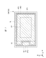
本実施の形態1による半導体装置の構成について、図1を用いて説明する。
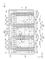
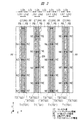
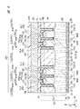
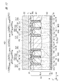
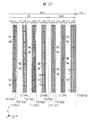
本実施の形態1による半導体装置のセル形成領域の構成について、図2〜図4を用いて説明する。
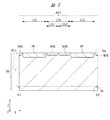
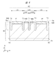
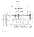
次に、本実施の形態1による半導体装置の製造方法について、図5〜図10を用いて説明する。
次に、本発明者らが検討した比較例による半導体装置のセル形成領域の構成について、図11および図12を用いて説明する。
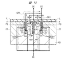
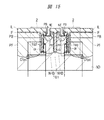
次に、比較例による半導体装置の特長について、図13および図14を用いて説明する。
一方、比較例による半導体装置は、課題も有する。以下では、比較例による半導体装置の課題について説明する。
次に、本実施の形態1による半導体装置の主要な特長と効果について、図21および図22を用いて説明する。
本実施の形態1の変形例による半導体装置に備わるIE型トレンチゲートIGBTの構成について、図23および図24を用いて説明する。
本実施の形態1の変形例による半導体装置でも、前述の実施の形態1による半導体装置と同様に、セル形成領域AR1には、平面視において、複数のn+型エミッタ領域NEが千鳥配置されている。
<比較例による半導体装置の構成と課題>
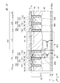
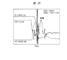
まず、本発明者らが検討した比較例による半導体装置のセル形成領域の構成について、図25および図26を用いて説明する。
以下、セル形成領域AR1のX軸方向の端部領域に設けられたダミーセル形成領域DAを有効に活用することのできる、本実施の形態2による半導体装置のセル形成領域の構成について、図27および図28を用いて説明する。
本実施の形態2による半導体装置の第1例では、セル形成領域AR1のX軸方向の端部に位置する端部領域DA1に、複数のn+型エミッタ領域NEを配置することにより、端部領域DA1を有効に活用することができる。ただし、端部領域DA1において、電流集中が起きないようにするため、端部領域DA1に配置される複数のn+型エミッタ領域NEの密度は、セル形成領域AR1の活性領域CAに配置されるn+型エミッタ領域NEの密度よりも低くする必要がある。すなわち、セル形成領域AR1の端部領域DA1に配置される複数のn+型エミッタ領域NEのY軸方向の間隔SD1は、セル形成領域AR1の活性領域CAに配置される複数のn+型エミッタ領域NEのY軸方向の間隔S1よりも大きくする必要がある。
<本実施の形態3によるモジュールの構成>
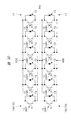
本実施の形態3では、前述の実施の形態1による半導体装置を備えた半導体チップを複数個有し、当該複数個の半導体チップが互いに並列に接続されたモジュールである例について説明する。
前述したように、本実施の形態3のモジュールであるIGBTモジュール10に含まれる複数のIGBTチップ12の各々として、前述の実施の形態1による半導体装置を用いることができる。
2 寄生MOSFET
10、10H、10L IGBTモジュール
11 ダイオードモジュール
12 IGBTチップ
13 ダイオード
AR1 セル形成領域
AR2 ゲート配線引き出し領域
AR3 領域
BP1 第1寄生pnpバイポーラトランジスタ
BP2 第2寄生pnpバイポーラトランジスタ
BR 領域
CA 活性領域
CE コレクタ電極
CF 導電性膜
CHP 半導体チップ
CL p+型コレクタ領域
CP 接続電極
CR1、CR2 変位電流
CT コンタクト溝
CTC1、CTC2 制御回路
CTE 接続電極
DA ダミーセル形成領域
DA1、DA2 端部領域
EE エミッタ電極
EP エミッタパッド
FPF 絶縁膜
GE ゲート電極
GI ゲート絶縁膜
GL ゲート配線
GND 接地電位
GP ゲートパッド
GTG 接続電極
IF 絶縁膜
IL 層間絶縁膜
INV インバータ
LCh ハイブリッドセル領域(アクティブセル領域)
LCh1、LCh2 ハイブリッドサブセル領域
LCi インアクティブセル領域
MOT モータ
ND n−型ドリフト領域
NE n+型エミッタ領域
NHB n型ホールバリア領域
Ns n型フィールドストップ領域
OP1、OP2 開口部
PB p型ボディ領域
PBC、PBCp p+型ボディコンタクト領域
PF、PFp p型フローティング領域
PH1 U相
PH2 V相
PH3 W相
PLP p+型ラッチアップ防止領域
PM1、PM2 パワーモジュール
PR p+型半導体領域
PR1 素子部
PR2 介在部
PT101 電流経路
Sa 上面
Sb 下面
SD1、SD2 間隔
SLn、SLp 半導体層
SS 半導体基板
T1、T2、T3 トレンチ
TA ターミネーション領域
TG1、TG2、TG3 トレンチ電極
TGp 端部トレンチ電極
TGx エミッタ接続部
TGz トレンチ電極
TM1、TM2 入力端子
VCC 電源電位
Wh、Wh1、Wh2、Wi、Wp、Wcp 幅
Claims (11)
- 第1主面および前記第1主面と反対側の第2主面を有する半導体基板と、
前記半導体基板の内部に形成された第1導電型の第1半導体層と、
前記第1半導体層と前記第2主面との間の前記半導体基板に形成された、前記第1導電型と異なる第2導電型の第2半導体層と、
平面視において、前記半導体基板の中央部に設けられたセル形成領域と、
平面視において、前記セル形成領域の外側に設けられたターミネーション領域と、
前記セル形成領域の前記半導体基板の前記第1主面側に、平面視において、第1方向に互いに離間して設けられ、前記第1方向と直交する第2方向に延在する複数の素子部と、
前記セル形成領域の前記半導体基板の前記第1主面側に、平面視において、前記複数の素子部のそれぞれの間に設けられた複数の介在部と、
を備え、
前記複数の素子部のそれぞれは、
前記第1主面から前記第1半導体層の途中まで達し、前記素子部と前記介在部との一方の境部に設けられ、平面視において、前記第2方向に延在する第1溝と、
前記第1主面から前記第1半導体層の途中まで達し、前記素子部と前記介在部との他方の境部に設けられ、平面視において、前記第2方向に延在する第2溝と、
前記第1主面から前記第1半導体層の途中まで達し、前記第1溝と前記第2溝との間に設けられ、平面視において、前記第2方向に延在する第3溝と、
前記第1溝の内部に第1絶縁膜を介して埋め込まれた第1トレンチ電極と、
前記第2溝の内部に第2絶縁膜を介して埋め込まれた第2トレンチ電極と、
前記第3溝の内部に第3絶縁膜を介して埋め込まれた第3トレンチ電極と、
前記第1溝と前記第3溝との間の前記半導体基板の前記第1主面側に形成され、前記第1絶縁膜および前記第3絶縁膜に接触する、前記第2導電型の第1半導体領域と、
前記第2溝と前記第3溝との間の前記半導体基板の前記第1主面側に形成され、前記第2絶縁膜および前記第3絶縁膜に接触する、前記第2導電型の第2半導体領域と、
前記第1半導体領域の途中まで達し、前記第1溝と前記第3溝との間に設けられ、平面視において、前記第2方向に延在する第1接続部と、
前記第2半導体領域の途中まで達し、前記第2溝と前記第3溝との間に設けられ、平面視において、前記第2方向に延在する第2接続部と、
前記第1接続部と前記第3溝との間および前記第2接続部と前記第3溝との間の前記半導体基板の前記第1主面側に、前記第1接続部および前記第2接続部の深さより浅く形成され、前記第3絶縁膜に接触し、平面視において、前記第2方向に互いに一定の間隔で配置された複数の前記第1導電型の第3半導体領域と、
を有し、
前記複数の介在部のそれぞれは、
前記第1主面から前記第1半導体層に達する、前記第2導電型の第4半導体領域、
を有し、
前記セル形成領域は、
平面視において、前記セル形成領域の中央部に位置する第1領域と、
平面視において、前記第1領域と前記ターミネーション領域との間に位置する第2領域と、
を有し、
前記第1領域の前記素子部に形成された複数の前記第3半導体領域は、前記第2方向に第1間隔で配置され、前記第2領域の前記素子部に形成された複数の前記第3半導体領域は、前記第2方向に第2間隔で配置され、前記第2間隔は、前記第1間隔よりも大きく、
前記第1領域では、前記介在部を挟んで、前記第1方向に互いに隣り合う2つの前記素子部において、一方の前記素子部に形成された複数の前記第3半導体領域のうち、前記第2方向に互いに隣り合う2つの前記第3半導体領域に挟まれた領域の前記第1方向に、他方の前記素子部に形成された複数の前記第3半導体領域のうち、1つの前記第3半導体領域が配置されている、半導体装置。 - 請求項1記載の半導体装置において、
前記第2領域では、前記介在部を挟んで、前記第1方向に互いに隣り合う2つの前記素子部において、一方の前記素子部に形成された複数の前記第3半導体領域のうち、前記第2方向に互いに隣り合う2つの前記第3半導体領域に挟まれた領域の前記第1方向に、他方の前記素子部に形成された複数の前記第3半導体領域のうち、1つの前記第3半導体領域が配置されている、半導体装置。 - 請求項2記載の半導体装置において、
前記第1領域では、前記第1方向に互いに隣り合う2つの前記素子部において、一方の前記素子部に形成された複数の前記第3半導体領域のうち、前記第2方向に互いに隣り合う2つの前記第3半導体領域の前記第1間隔の半分の位置の前記第1方向に、他方の前記素子部に形成された複数の第3半導体領域のうち、1つの前記第3半導体領域が配置され、
前記第2領域では、前記第1方向に互いに隣り合う2つの前記素子部において、一方の前記素子部に形成された複数の前記第3半導体領域のうち、前記第2方向に互いに隣り合う2つの前記第3半導体領域の前記第2間隔の半分の位置の前記第1方向に、他方の前記素子部に形成された複数の第3半導体領域のうち、1つの前記第3半導体領域が配置されている、半導体装置。 - 請求項2記載の半導体装置において、
前記第1領域および前記第2領域ではそれぞれ、平面視において、複数の前記第3半導体領域は千鳥配置されている、半導体装置。 - 請求項2記載の半導体装置において、
前記第1領域および前記第2領域ではそれぞれ、平面視において、三角形の各頂点に前記第3半導体領域が位置する基本パターンが連続して配列されている、半導体装置。 - 請求項2記載の半導体装置において、
前記第1領域および前記第2領域ではそれぞれ、前記第1方向に互いに隣り合う2つの前記素子部のそれぞれに形成された複数の前記第3半導体領域は、前記第1方向に互いに隣り合う2つの前記素子部の間に位置する前記介在部を挟んで非対称に配置されている、半導体装置。 - 請求項1記載の半導体装置において、
前記第2領域では、前記第1方向に互いに隣り合う2つの前記素子部のそれぞれに形成された複数の前記第3半導体領域は、前記第1方向に互いに隣り合う2つの前記素子部の間に位置する前記介在部を挟んで対称に配置されている、半導体装置。 - 請求項7記載の半導体装置において、
前記第1領域では、前記第1方向に互いに隣り合う2つの前記素子部において、一方の前記素子部に形成された複数の前記第3半導体領域のうち、前記第2方向に互いに隣り合う2つの前記第3半導体領域の前記第1間隔の半分の位置の前記第1方向に、他方の前記素子部に形成された複数の第3半導体領域のうち、1つの前記第3半導体領域が配置されている、半導体装置。 - 請求項7記載の半導体装置において、
前記第1領域では、平面視において、複数の前記第3半導体領域は千鳥配置されている、半導体装置。 - 請求項7記載の半導体装置において、
前記第1領域では、平面視において、三角形の各頂点に前記第3半導体領域が位置する基本パターンが連続して配列されている、半導体装置。 - 請求項7記載の半導体装置において、
前記第1領域では、前記第1方向に互いに隣り合う2つの前記素子部のそれぞれに形成されている前記複数の第3半導体領域は、前記第1方向に互いに隣り合う2つの前記素子部の間に位置する前記介在部を挟んで非対称に配置されている、半導体装置。
Priority Applications (5)
| Application Number | Priority Date | Filing Date | Title |
|---|---|---|---|
| JP2016227933A JP6797005B2 (ja) | 2016-11-24 | 2016-11-24 | 半導体装置 |
| US15/706,554 US10115793B2 (en) | 2016-11-24 | 2017-09-15 | Semiconductor device |
| EP17191763.6A EP3327787B1 (en) | 2016-11-24 | 2017-09-19 | Semiconductor device |
| TW106140197A TWI749107B (zh) | 2016-11-24 | 2017-11-21 | 半導體裝置 |
| CN201711182135.4A CN108110001B (zh) | 2016-11-24 | 2017-11-23 | 半导体器件 |
Applications Claiming Priority (1)
| Application Number | Priority Date | Filing Date | Title |
|---|---|---|---|
| JP2016227933A JP6797005B2 (ja) | 2016-11-24 | 2016-11-24 | 半導体装置 |
Publications (2)
| Publication Number | Publication Date |
|---|---|
| JP2018085449A JP2018085449A (ja) | 2018-05-31 |
| JP6797005B2 true JP6797005B2 (ja) | 2020-12-09 |
Family
ID=59914343
Family Applications (1)
| Application Number | Title | Priority Date | Filing Date |
|---|---|---|---|
| JP2016227933A Active JP6797005B2 (ja) | 2016-11-24 | 2016-11-24 | 半導体装置 |
Country Status (5)
| Country | Link |
|---|---|
| US (1) | US10115793B2 (ja) |
| EP (1) | EP3327787B1 (ja) |
| JP (1) | JP6797005B2 (ja) |
| CN (1) | CN108110001B (ja) |
| TW (1) | TWI749107B (ja) |
Families Citing this family (6)
| Publication number | Priority date | Publication date | Assignee | Title |
|---|---|---|---|---|
| JP2018022776A (ja) * | 2016-08-03 | 2018-02-08 | ルネサスエレクトロニクス株式会社 | 半導体装置 |
| JP6909666B2 (ja) * | 2017-07-27 | 2021-07-28 | ルネサスエレクトロニクス株式会社 | 半導体装置およびその製造方法 |
| DE102017125666A1 (de) | 2017-11-02 | 2019-05-02 | Elwema Automotive Gmbh | Vorrichtung und Verfahren zum Reinigen von Werkstücken mittels eines Dampfstrahls und Dampferzeuger hierfür |
| CN109713037B (zh) * | 2018-12-29 | 2021-11-23 | 安建科技(深圳)有限公司 | 一种绝缘栅双极性晶体管器件及其制备方法 |
| WO2022202370A1 (ja) * | 2021-03-26 | 2022-09-29 | 株式会社村田製作所 | 半導体装置 |
| JP2022167435A (ja) * | 2021-04-23 | 2022-11-04 | 株式会社 日立パワーデバイス | 半導体装置及びそれを用いた電力変換装置、半導体装置の製造方法 |
Family Cites Families (11)
| Publication number | Priority date | Publication date | Assignee | Title |
|---|---|---|---|---|
| JP3426928B2 (ja) * | 1996-09-18 | 2003-07-14 | 株式会社東芝 | 電力用半導体装置 |
| JP3984227B2 (ja) | 2004-01-15 | 2007-10-03 | 株式会社東芝 | 半導体装置 |
| JP4857566B2 (ja) * | 2005-01-27 | 2012-01-18 | 富士電機株式会社 | 絶縁ゲート型半導体装置とその製造方法 |
| US7943990B2 (en) * | 2005-08-17 | 2011-05-17 | International Rectifier Corporation | Power semiconductor device with interconnected gate trenches |
| WO2011111500A1 (ja) | 2010-03-09 | 2011-09-15 | 富士電機システムズ株式会社 | 半導体装置 |
| JP5732790B2 (ja) * | 2010-09-14 | 2015-06-10 | 株式会社デンソー | 炭化珪素半導体装置およびその製造方法 |
| JP5609939B2 (ja) * | 2011-09-27 | 2014-10-22 | 株式会社デンソー | 半導体装置 |
| JP5973730B2 (ja) | 2012-01-05 | 2016-08-23 | ルネサスエレクトロニクス株式会社 | Ie型トレンチゲートigbt |
| JP2014011418A (ja) | 2012-07-03 | 2014-01-20 | Hitachi Ltd | 半導体装置およびその製造方法 |
| JP2014075582A (ja) | 2012-09-12 | 2014-04-24 | Fuji Electric Co Ltd | 半導体装置および半導体装置の製造方法 |
| JP6448434B2 (ja) * | 2015-03-25 | 2019-01-09 | ルネサスエレクトロニクス株式会社 | 半導体装置およびその製造方法 |
-
2016
- 2016-11-24 JP JP2016227933A patent/JP6797005B2/ja active Active
-
2017
- 2017-09-15 US US15/706,554 patent/US10115793B2/en active Active
- 2017-09-19 EP EP17191763.6A patent/EP3327787B1/en active Active
- 2017-11-21 TW TW106140197A patent/TWI749107B/zh active
- 2017-11-23 CN CN201711182135.4A patent/CN108110001B/zh active Active
Also Published As
| Publication number | Publication date |
|---|---|
| US10115793B2 (en) | 2018-10-30 |
| US20180145134A1 (en) | 2018-05-24 |
| TWI749107B (zh) | 2021-12-11 |
| EP3327787A1 (en) | 2018-05-30 |
| EP3327787B1 (en) | 2019-07-24 |
| JP2018085449A (ja) | 2018-05-31 |
| TW201832320A (zh) | 2018-09-01 |
| CN108110001A (zh) | 2018-06-01 |
| CN108110001B (zh) | 2023-07-14 |
Similar Documents
| Publication | Publication Date | Title |
|---|---|---|
| US10998432B2 (en) | Semiconductor device and method of manufacturing the same | |
| JP6584893B2 (ja) | 半導体装置の製造方法 | |
| JP6448434B2 (ja) | 半導体装置およびその製造方法 | |
| JP6797005B2 (ja) | 半導体装置 | |
| JP2015065420A (ja) | 半導体装置 | |
| JP6963982B2 (ja) | 半導体装置およびその製造方法 | |
| JP2018182254A (ja) | 半導体装置およびその製造方法 | |
| JP4167294B2 (ja) | 半導体素子及び電気機器 | |
| WO2007013367A1 (ja) | 半導体素子及び電気機器 | |
| JP2019106409A (ja) | 半導体装置およびその製造方法 | |
| US10134887B2 (en) | Semiconductor device and manufacturing method thereof | |
| JP2020004864A (ja) | 半導体装置 |
Legal Events
| Date | Code | Title | Description |
|---|---|---|---|
| A621 | Written request for application examination |
Free format text: JAPANESE INTERMEDIATE CODE: A621 Effective date: 20190405 |
|
| A131 | Notification of reasons for refusal |
Free format text: JAPANESE INTERMEDIATE CODE: A131 Effective date: 20200204 |
|
| A977 | Report on retrieval |
Free format text: JAPANESE INTERMEDIATE CODE: A971007 Effective date: 20200131 |
|
| A521 | Request for written amendment filed |
Free format text: JAPANESE INTERMEDIATE CODE: A523 Effective date: 20200402 |
|
| A02 | Decision of refusal |
Free format text: JAPANESE INTERMEDIATE CODE: A02 Effective date: 20200616 |
|
| A521 | Request for written amendment filed |
Free format text: JAPANESE INTERMEDIATE CODE: A523 Effective date: 20200911 |
|
| C60 | Trial request (containing other claim documents, opposition documents) |
Free format text: JAPANESE INTERMEDIATE CODE: C60 Effective date: 20200911 |
|
| A911 | Transfer to examiner for re-examination before appeal (zenchi) |
Free format text: JAPANESE INTERMEDIATE CODE: A911 Effective date: 20200923 |
|
| C21 | Notice of transfer of a case for reconsideration by examiners before appeal proceedings |
Free format text: JAPANESE INTERMEDIATE CODE: C21 Effective date: 20200929 |
|
| TRDD | Decision of grant or rejection written | ||
| A01 | Written decision to grant a patent or to grant a registration (utility model) |
Free format text: JAPANESE INTERMEDIATE CODE: A01 Effective date: 20201027 |
|
| A61 | First payment of annual fees (during grant procedure) |
Free format text: JAPANESE INTERMEDIATE CODE: A61 Effective date: 20201117 |
|
| R150 | Certificate of patent or registration of utility model |
Ref document number: 6797005 Country of ref document: JP Free format text: JAPANESE INTERMEDIATE CODE: R150 |