JP6806787B2 - ナノポアセンシングのための絶縁体−膜−絶縁体デバイスのウェハスケールアセンブリ - Google Patents
ナノポアセンシングのための絶縁体−膜−絶縁体デバイスのウェハスケールアセンブリ Download PDFInfo
- Publication number
- JP6806787B2 JP6806787B2 JP2018549559A JP2018549559A JP6806787B2 JP 6806787 B2 JP6806787 B2 JP 6806787B2 JP 2018549559 A JP2018549559 A JP 2018549559A JP 2018549559 A JP2018549559 A JP 2018549559A JP 6806787 B2 JP6806787 B2 JP 6806787B2
- Authority
- JP
- Japan
- Prior art keywords
- nanopore
- channel
- fluid channel
- layer
- membrane
- Prior art date
- Legal status (The legal status is an assumption and is not a legal conclusion. Google has not performed a legal analysis and makes no representation as to the accuracy of the status listed.)
- Active
Links
- 0 C(C1)CC1N1C*C1 Chemical compound C(C1)CC1N1C*C1 0.000 description 1
Images


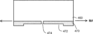


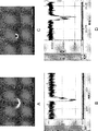


Classifications
-
- G—PHYSICS
- G01—MEASURING; TESTING
- G01N—INVESTIGATING OR ANALYSING MATERIALS BY DETERMINING THEIR CHEMICAL OR PHYSICAL PROPERTIES
- G01N33/00—Investigating or analysing materials by specific methods not covered by groups G01N1/00 - G01N31/00
- G01N33/48—Biological material, e.g. blood, urine; Haemocytometers
- G01N33/483—Physical analysis of biological material
- G01N33/487—Physical analysis of biological material of liquid biological material
- G01N33/48707—Physical analysis of biological material of liquid biological material by electrical means
- G01N33/48721—Investigating individual macromolecules, e.g. by translocation through nanopores
-
- B—PERFORMING OPERATIONS; TRANSPORTING
- B01—PHYSICAL OR CHEMICAL PROCESSES OR APPARATUS IN GENERAL
- B01L—CHEMICAL OR PHYSICAL LABORATORY APPARATUS FOR GENERAL USE
- B01L3/00—Containers or dishes for laboratory use, e.g. laboratory glassware; Droppers
- B01L3/50—Containers for the purpose of retaining a material to be analysed, e.g. test tubes
- B01L3/502—Containers for the purpose of retaining a material to be analysed, e.g. test tubes with fluid transport, e.g. in multi-compartment structures
- B01L3/5027—Containers for the purpose of retaining a material to be analysed, e.g. test tubes with fluid transport, e.g. in multi-compartment structures by integrated microfluidic structures, i.e. dimensions of channels and chambers are such that surface tension forces are important, e.g. lab-on-a-chip
- B01L3/502707—Containers for the purpose of retaining a material to be analysed, e.g. test tubes with fluid transport, e.g. in multi-compartment structures by integrated microfluidic structures, i.e. dimensions of channels and chambers are such that surface tension forces are important, e.g. lab-on-a-chip characterised by the manufacture of the container or its components
-
- B—PERFORMING OPERATIONS; TRANSPORTING
- B01—PHYSICAL OR CHEMICAL PROCESSES OR APPARATUS IN GENERAL
- B01L—CHEMICAL OR PHYSICAL LABORATORY APPARATUS FOR GENERAL USE
- B01L3/00—Containers or dishes for laboratory use, e.g. laboratory glassware; Droppers
- B01L3/50—Containers for the purpose of retaining a material to be analysed, e.g. test tubes
- B01L3/502—Containers for the purpose of retaining a material to be analysed, e.g. test tubes with fluid transport, e.g. in multi-compartment structures
- B01L3/5027—Containers for the purpose of retaining a material to be analysed, e.g. test tubes with fluid transport, e.g. in multi-compartment structures by integrated microfluidic structures, i.e. dimensions of channels and chambers are such that surface tension forces are important, e.g. lab-on-a-chip
- B01L3/502715—Containers for the purpose of retaining a material to be analysed, e.g. test tubes with fluid transport, e.g. in multi-compartment structures by integrated microfluidic structures, i.e. dimensions of channels and chambers are such that surface tension forces are important, e.g. lab-on-a-chip characterised by interfacing components, e.g. fluidic, electrical, optical or mechanical interfaces
-
- B—PERFORMING OPERATIONS; TRANSPORTING
- B81—MICROSTRUCTURAL TECHNOLOGY
- B81C—PROCESSES OR APPARATUS SPECIALLY ADAPTED FOR THE MANUFACTURE OR TREATMENT OF MICROSTRUCTURAL DEVICES OR SYSTEMS
- B81C1/00—Manufacture or treatment of devices or systems in or on a substrate
- B81C1/00015—Manufacture or treatment of devices or systems in or on a substrate for manufacturing microsystems
- B81C1/00023—Manufacture or treatment of devices or systems in or on a substrate for manufacturing microsystems without movable or flexible elements
- B81C1/00119—Arrangement of basic structures like cavities or channels, e.g. suitable for microfluidic systems
-
- G—PHYSICS
- G01—MEASURING; TESTING
- G01N—INVESTIGATING OR ANALYSING MATERIALS BY DETERMINING THEIR CHEMICAL OR PHYSICAL PROPERTIES
- G01N27/00—Investigating or analysing materials by the use of electric, electrochemical, or magnetic means
- G01N27/26—Investigating or analysing materials by the use of electric, electrochemical, or magnetic means by investigating electrochemical variables; by using electrolysis or electrophoresis
- G01N27/28—Electrolytic cell components
- G01N27/30—Electrodes, e.g. test electrodes; Half-cells
- G01N27/327—Biochemical electrodes, e.g. electrical or mechanical details for in vitro measurements
- G01N27/3275—Sensing specific biomolecules, e.g. nucleic acid strands, based on an electrode surface reaction
- G01N27/3278—Sensing specific biomolecules, e.g. nucleic acid strands, based on an electrode surface reaction involving nanosized elements, e.g. nanogaps or nanoparticles
-
- G—PHYSICS
- G01—MEASURING; TESTING
- G01N—INVESTIGATING OR ANALYSING MATERIALS BY DETERMINING THEIR CHEMICAL OR PHYSICAL PROPERTIES
- G01N27/00—Investigating or analysing materials by the use of electric, electrochemical, or magnetic means
- G01N27/26—Investigating or analysing materials by the use of electric, electrochemical, or magnetic means by investigating electrochemical variables; by using electrolysis or electrophoresis
- G01N27/416—Systems
- G01N27/447—Systems using electrophoresis
- G01N27/44756—Apparatus specially adapted therefor
- G01N27/44791—Microapparatus
-
- H—ELECTRICITY
- H10—SEMICONDUCTOR DEVICES; ELECTRIC SOLID-STATE DEVICES NOT OTHERWISE PROVIDED FOR
- H10P—GENERIC PROCESSES OR APPARATUS FOR THE MANUFACTURE OR TREATMENT OF DEVICES COVERED BY CLASS H10
- H10P72/00—Handling or holding of wafers, substrates or devices during manufacture or treatment thereof
- H10P72/06—Apparatus for monitoring, sorting, marking, testing or measuring
-
- B—PERFORMING OPERATIONS; TRANSPORTING
- B01—PHYSICAL OR CHEMICAL PROCESSES OR APPARATUS IN GENERAL
- B01L—CHEMICAL OR PHYSICAL LABORATORY APPARATUS FOR GENERAL USE
- B01L2200/00—Solutions for specific problems relating to chemical or physical laboratory apparatus
- B01L2200/02—Adapting objects or devices to another
- B01L2200/025—Align devices or objects to ensure defined positions relative to each other
-
- B—PERFORMING OPERATIONS; TRANSPORTING
- B01—PHYSICAL OR CHEMICAL PROCESSES OR APPARATUS IN GENERAL
- B01L—CHEMICAL OR PHYSICAL LABORATORY APPARATUS FOR GENERAL USE
- B01L2200/00—Solutions for specific problems relating to chemical or physical laboratory apparatus
- B01L2200/02—Adapting objects or devices to another
- B01L2200/026—Fluid interfacing between devices or objects, e.g. connectors, inlet details
- B01L2200/027—Fluid interfacing between devices or objects, e.g. connectors, inlet details for microfluidic devices
-
- B—PERFORMING OPERATIONS; TRANSPORTING
- B01—PHYSICAL OR CHEMICAL PROCESSES OR APPARATUS IN GENERAL
- B01L—CHEMICAL OR PHYSICAL LABORATORY APPARATUS FOR GENERAL USE
- B01L2200/00—Solutions for specific problems relating to chemical or physical laboratory apparatus
- B01L2200/14—Process control and prevention of errors
-
- B—PERFORMING OPERATIONS; TRANSPORTING
- B01—PHYSICAL OR CHEMICAL PROCESSES OR APPARATUS IN GENERAL
- B01L—CHEMICAL OR PHYSICAL LABORATORY APPARATUS FOR GENERAL USE
- B01L2300/00—Additional constructional details
- B01L2300/06—Auxiliary integrated devices, integrated components
- B01L2300/0627—Sensor or part of a sensor is integrated
- B01L2300/0645—Electrodes
-
- B—PERFORMING OPERATIONS; TRANSPORTING
- B81—MICROSTRUCTURAL TECHNOLOGY
- B81B—MICROSTRUCTURAL DEVICES OR SYSTEMS, e.g. MICROMECHANICAL DEVICES
- B81B2201/00—Specific applications of microelectromechanical systems
- B81B2201/02—Sensors
- B81B2201/0214—Biosensors; Chemical sensors
-
- B—PERFORMING OPERATIONS; TRANSPORTING
- B81—MICROSTRUCTURAL TECHNOLOGY
- B81B—MICROSTRUCTURAL DEVICES OR SYSTEMS, e.g. MICROMECHANICAL DEVICES
- B81B2201/00—Specific applications of microelectromechanical systems
- B81B2201/05—Microfluidics
- B81B2201/058—Microfluidics not provided for in B81B2201/051 - B81B2201/054
-
- B—PERFORMING OPERATIONS; TRANSPORTING
- B81—MICROSTRUCTURAL TECHNOLOGY
- B81B—MICROSTRUCTURAL DEVICES OR SYSTEMS, e.g. MICROMECHANICAL DEVICES
- B81B2203/00—Basic microelectromechanical structures
- B81B2203/03—Static structures
- B81B2203/0353—Holes
-
- B—PERFORMING OPERATIONS; TRANSPORTING
- B81—MICROSTRUCTURAL TECHNOLOGY
- B81C—PROCESSES OR APPARATUS SPECIALLY ADAPTED FOR THE MANUFACTURE OR TREATMENT OF MICROSTRUCTURAL DEVICES OR SYSTEMS
- B81C2203/00—Forming microstructural systems
- B81C2203/03—Bonding two components
- B81C2203/031—Anodic bondings
-
- B—PERFORMING OPERATIONS; TRANSPORTING
- B81—MICROSTRUCTURAL TECHNOLOGY
- B81C—PROCESSES OR APPARATUS SPECIALLY ADAPTED FOR THE MANUFACTURE OR TREATMENT OF MICROSTRUCTURAL DEVICES OR SYSTEMS
- B81C2203/00—Forming microstructural systems
- B81C2203/03—Bonding two components
- B81C2203/033—Thermal bonding
- B81C2203/035—Soldering
-
- B—PERFORMING OPERATIONS; TRANSPORTING
- B81—MICROSTRUCTURAL TECHNOLOGY
- B81C—PROCESSES OR APPARATUS SPECIALLY ADAPTED FOR THE MANUFACTURE OR TREATMENT OF MICROSTRUCTURAL DEVICES OR SYSTEMS
- B81C2203/00—Forming microstructural systems
- B81C2203/03—Bonding two components
- B81C2203/033—Thermal bonding
- B81C2203/036—Fusion bonding
Landscapes
- Health & Medical Sciences (AREA)
- Chemical & Material Sciences (AREA)
- Engineering & Computer Science (AREA)
- Life Sciences & Earth Sciences (AREA)
- Physics & Mathematics (AREA)
- Biomedical Technology (AREA)
- Analytical Chemistry (AREA)
- General Health & Medical Sciences (AREA)
- Molecular Biology (AREA)
- Hematology (AREA)
- Biochemistry (AREA)
- Pathology (AREA)
- Immunology (AREA)
- General Physics & Mathematics (AREA)
- Chemical Kinetics & Catalysis (AREA)
- Dispersion Chemistry (AREA)
- Nanotechnology (AREA)
- Spectroscopy & Molecular Physics (AREA)
- Urology & Nephrology (AREA)
- Food Science & Technology (AREA)
- Biophysics (AREA)
- Medicinal Chemistry (AREA)
- Clinical Laboratory Science (AREA)
- Electrochemistry (AREA)
- Manufacturing & Machinery (AREA)
- Microelectronics & Electronic Packaging (AREA)
- Investigating Or Analyzing Materials By The Use Of Electric Means (AREA)
- Micromachines (AREA)
- Apparatus Associated With Microorganisms And Enzymes (AREA)
- Physical Or Chemical Processes And Apparatus (AREA)
Applications Claiming Priority (5)
| Application Number | Priority Date | Filing Date | Title |
|---|---|---|---|
| US201662311294P | 2016-03-21 | 2016-03-21 | |
| US62/311,294 | 2016-03-21 | ||
| US201662356303P | 2016-06-29 | 2016-06-29 | |
| US62/356,303 | 2016-06-29 | ||
| PCT/US2017/023149 WO2017165267A1 (en) | 2016-03-21 | 2017-03-20 | Wafer-scale assembly of insulator-membrane-insulator devices for nanopore sensing |
Related Child Applications (1)
| Application Number | Title | Priority Date | Filing Date |
|---|---|---|---|
| JP2020201428A Division JP2021056229A (ja) | 2016-03-21 | 2020-12-04 | ナノポアセンシングのための絶縁体−膜−絶縁体デバイスのウェハスケールアセンブリ |
Publications (3)
| Publication Number | Publication Date |
|---|---|
| JP2019516951A JP2019516951A (ja) | 2019-06-20 |
| JP2019516951A5 JP2019516951A5 (da) | 2020-04-23 |
| JP6806787B2 true JP6806787B2 (ja) | 2021-01-06 |
Family
ID=59899703
Family Applications (2)
| Application Number | Title | Priority Date | Filing Date |
|---|---|---|---|
| JP2018549559A Active JP6806787B2 (ja) | 2016-03-21 | 2017-03-20 | ナノポアセンシングのための絶縁体−膜−絶縁体デバイスのウェハスケールアセンブリ |
| JP2020201428A Ceased JP2021056229A (ja) | 2016-03-21 | 2020-12-04 | ナノポアセンシングのための絶縁体−膜−絶縁体デバイスのウェハスケールアセンブリ |
Family Applications After (1)
| Application Number | Title | Priority Date | Filing Date |
|---|---|---|---|
| JP2020201428A Ceased JP2021056229A (ja) | 2016-03-21 | 2020-12-04 | ナノポアセンシングのための絶縁体−膜−絶縁体デバイスのウェハスケールアセンブリ |
Country Status (9)
| Country | Link |
|---|---|
| US (2) | US10488394B2 (da) |
| EP (2) | EP3936863A1 (da) |
| JP (2) | JP6806787B2 (da) |
| KR (1) | KR102205435B1 (da) |
| CN (1) | CN108886053B (da) |
| AU (1) | AU2017237981B2 (da) |
| CA (1) | CA3018069C (da) |
| DK (1) | DK3440703T3 (da) |
| WO (1) | WO2017165267A1 (da) |
Families Citing this family (25)
| Publication number | Priority date | Publication date | Assignee | Title |
|---|---|---|---|---|
| KR102205435B1 (ko) * | 2016-03-21 | 2021-01-21 | 온테라 인크. | 나노기공 감지를 위한 절연체-막-절연체 장치의 웨이퍼-척도 어셈블리 |
| US10618805B2 (en) * | 2017-09-22 | 2020-04-14 | Applied Materials, Inc. | Method to reduce pore diameter using atomic layer deposition and etching |
| NZ759671A (en) | 2018-02-16 | 2022-07-01 | Illumina Inc | Device for sequencing |
| JP7190558B2 (ja) * | 2018-09-14 | 2022-12-15 | アプライド マテリアルズ インコーポレイテッド | ナノポアを形成する方法およびその結果生じる構造 |
| US11249067B2 (en) | 2018-10-29 | 2022-02-15 | Applied Materials, Inc. | Nanopore flow cells and methods of fabrication |
| WO2020138021A1 (ja) * | 2018-12-25 | 2020-07-02 | 国立大学法人大阪大学 | サンプル識別方法、サンプル識別用デバイス、および、サンプル識別装置 |
| CN114144664B (zh) * | 2019-04-24 | 2024-10-22 | 辛辛那提大学 | 基于介电性质的纳米囊泡的无标记表征方法 |
| CN114222823A (zh) * | 2019-06-07 | 2022-03-22 | 应用材料公司 | 用于制造双孔传感器的方法 |
| WO2020247071A1 (en) * | 2019-06-07 | 2020-12-10 | Applied Materials, Inc. | Dual pore sensors |
| US20210148885A1 (en) * | 2019-11-18 | 2021-05-20 | Nooma Bio, Inc. | Compact Multipore Array with Embedded Electrodes for Sample Analysis |
| CN111122398A (zh) * | 2019-12-20 | 2020-05-08 | 瑞芯智造(深圳)科技有限公司 | 一种微纳颗粒的检测装置及方法 |
| US11536708B2 (en) | 2020-01-09 | 2022-12-27 | Applied Materials, Inc. | Methods to fabricate dual pore devices |
| WO2021178477A1 (en) | 2020-03-03 | 2021-09-10 | Arizona Board Of Regents On Behalf Of Arizona State University | Low-capacitance nanopore sensors on insulating substrates |
| DE102020202767B3 (de) * | 2020-03-04 | 2021-05-27 | Hahn-Schickard-Gesellschaft für angewandte Forschung e.V. | Herstellung eines Verbunds aus Polymersubstraten und gesiegelte mikrofluidische Kartusche |
| AU2021299182A1 (en) | 2020-07-02 | 2023-01-05 | Illumina, Inc. | Devices with field effect transistors |
| JPWO2022070669A1 (da) * | 2020-09-29 | 2022-04-07 | ||
| CN115125131A (zh) * | 2021-03-29 | 2022-09-30 | 上海近观科技有限责任公司 | 基于场效应晶体管的纳米孔阵列结构及其制备方法 |
| US12493024B2 (en) | 2021-03-31 | 2025-12-09 | Illumina, Inc. | Scalable circuit for molecular detection |
| US11711653B2 (en) | 2021-05-11 | 2023-07-25 | xMEMS Labs, Inc. | Sound producing cell and manufacturing method thereof |
| US12044646B2 (en) * | 2021-05-14 | 2024-07-23 | Taiwan Semiconductor Manufacturing Company Ltd. | Fluid sensor system |
| CN113552332B (zh) * | 2021-09-22 | 2022-04-22 | 成都齐碳科技有限公司 | 用于感测包含在液体中的分析物的装置和设备 |
| US12455277B2 (en) | 2021-09-30 | 2025-10-28 | Illumina, Inc. | Isolation of cells in a nanopore sensor array |
| US12063470B1 (en) * | 2023-02-10 | 2024-08-13 | xMEMS Labs, Inc. | Acoustic package structure and covering structure |
| WO2025154102A1 (en) * | 2024-01-19 | 2025-07-24 | Indian Institute Of Science | Nanopore device structure and fabrication method thereof |
| GB202407100D0 (en) * | 2024-05-17 | 2024-07-03 | Oxford Nanopore Tech Plc | A flow cell and a method |
Family Cites Families (47)
| Publication number | Priority date | Publication date | Assignee | Title |
|---|---|---|---|---|
| US6362002B1 (en) | 1995-03-17 | 2002-03-26 | President And Fellows Of Harvard College | Characterization of individual polymer molecules based on monomer-interface interactions |
| WO1998035012A2 (en) | 1997-02-12 | 1998-08-13 | Chan Eugene Y | Methods and products for analyzing polymers |
| US6267872B1 (en) | 1998-11-06 | 2001-07-31 | The Regents Of The University Of California | Miniature support for thin films containing single channels or nanopores and methods for using same |
| WO2000034527A2 (en) | 1998-12-11 | 2000-06-15 | The Regents Of The University Of California | Targeted molecular bar codes |
| US6783643B2 (en) | 1999-06-22 | 2004-08-31 | President And Fellows Of Harvard College | Control of solid state dimensional features |
| US7258838B2 (en) | 1999-06-22 | 2007-08-21 | President And Fellows Of Harvard College | Solid state molecular probe device |
| US6464842B1 (en) | 1999-06-22 | 2002-10-15 | President And Fellows Of Harvard College | Control of solid state dimensional features |
| EP2383776B1 (en) | 1999-06-22 | 2015-02-25 | President and Fellows of Harvard College | Solid state nanopore device for evaluating biopolymers |
| EP1212462B1 (en) | 1999-09-07 | 2006-01-25 | The Regents of the University of California | Methods of determining the presence of double stranded nucleic acids in a sample |
| WO2001059453A2 (en) | 2000-02-11 | 2001-08-16 | The Texas A & M University System | Biosensor compositions and methods of use |
| WO2002023964A1 (en) * | 2000-09-13 | 2002-03-21 | Applied Materials, Inc. | Processing chamber with multi-layer brazed lid |
| WO2002042496A2 (en) | 2000-11-27 | 2002-05-30 | The Regents Of The University Of California | Methods and devices for characterizing duplex nucleic acid molecules |
| US20030104428A1 (en) | 2001-06-21 | 2003-06-05 | President And Fellows Of Harvard College | Method for characterization of nucleic acid molecules |
| US7077152B2 (en) * | 2001-07-07 | 2006-07-18 | Nanostream, Inc. | Microfluidic metering systems and methods |
| WO2003047712A2 (en) * | 2001-10-18 | 2003-06-12 | The Board Of Trustees Of The University Of Illinois | Hybrid microfluidic and nanofluidic system |
| US20030180711A1 (en) * | 2002-02-21 | 2003-09-25 | Turner Stephen W. | Three dimensional microfluidic device having porous membrane |
| US6806543B2 (en) * | 2002-09-12 | 2004-10-19 | Intel Corporation | Microfluidic apparatus with integrated porous-substrate/sensor for real-time (bio)chemical molecule detection |
| US7279134B2 (en) * | 2002-09-17 | 2007-10-09 | Intel Corporation | Microfluidic devices with porous membranes for molecular sieving, metering, and separations |
| US7347921B2 (en) * | 2003-07-17 | 2008-03-25 | Agilent Technologies, Inc. | Apparatus and method for threading a biopolymer through a nanopore |
| US7075161B2 (en) * | 2003-10-23 | 2006-07-11 | Agilent Technologies, Inc. | Apparatus and method for making a low capacitance artificial nanopore |
| EP1783202B1 (en) * | 2004-08-25 | 2013-10-02 | Panasonic Corporation | Probe for measuring electric potential of cell |
| EP1970110B1 (en) * | 2005-12-28 | 2016-07-20 | Shimadzu Corporation | Gas exchange system and method of controlling pressure-diference bubble transfer |
| US10670559B2 (en) * | 2008-07-11 | 2020-06-02 | Cornell University | Nanofluidic channels with integrated charge sensors and methods based thereon |
| ES2672201T3 (es) * | 2008-07-16 | 2018-06-13 | Children's Medical Center Corporation | Dispositivo de imitación de órganos con microcanales y métodos de uso |
| US8169006B2 (en) * | 2008-11-29 | 2012-05-01 | Electronics And Telecommunications Research Institute | Bio-sensor chip for detecting target material |
| CA2768873A1 (en) * | 2009-07-23 | 2011-01-27 | Insight Nanofluidics Inc. | Nanofluidic cell |
| EP2533963A4 (en) * | 2010-02-11 | 2015-01-21 | Yung-Chieh Tan | SYSTEMS AND METHODS FOR MANUFACTURING MICROSTRUCTURES |
| CN102095768B (zh) * | 2010-11-16 | 2014-07-09 | 浙江大学 | 一种亚纳米厚度的纳米孔传感器 |
| US8518829B2 (en) * | 2011-04-22 | 2013-08-27 | International Business Machines Corporation | Self-sealed fluidic channels for nanopore array |
| EP3318872A1 (en) * | 2011-07-20 | 2018-05-09 | The Regents of the University of California | Dual-pore device |
| EP2578207A3 (en) * | 2011-10-05 | 2015-10-07 | Jacob J. Schmidt | Masking apertures enabling automation and solution exchange in sessile droplet lipid bilayers |
| US8696881B2 (en) * | 2011-10-21 | 2014-04-15 | Wisconsin Alumni Research Foundation | Patch-clamp providing on-chip thermal gradient |
| WO2013076943A1 (ja) * | 2011-11-22 | 2013-05-30 | パナソニック株式会社 | 生体分子の1分子検出方法および1分子検出装置、疾病マーカ検査装置 |
| KR101354480B1 (ko) * | 2012-05-14 | 2014-01-27 | 한국과학기술연구원 | 나노채널과 결합된 나노포어를 이용한 입자 검출 장치 및 방법 |
| KR20130143429A (ko) * | 2012-06-21 | 2013-12-31 | 서울대학교산학협력단 | 수직적 나노 채널 및 나노 포어를 가지는 이온 소자 |
| US10065154B2 (en) * | 2012-10-05 | 2018-09-04 | Massachusetts Institute Of Technology | Nanofluidic sorting system for gene synthesis and pcr reaction products |
| US9372171B2 (en) * | 2013-04-30 | 2016-06-21 | International Business Machines Corporation | Nanopore sensor for detecting molecular interactions |
| US9846141B2 (en) * | 2014-04-30 | 2017-12-19 | International Business Machines Corporation | Presenting stretched strands of single strand DNA for sequencing double strand DNA |
| JP6258145B2 (ja) * | 2014-07-18 | 2018-01-10 | 株式会社東芝 | 微粒子検査システム及びその駆動方法 |
| JP6285040B2 (ja) * | 2014-09-11 | 2018-02-28 | 株式会社日立製作所 | 生体分子構造解析用デバイスおよび生体分子構造解析用デバイスの形成方法 |
| WO2016196625A1 (en) | 2015-06-02 | 2016-12-08 | Nanopore Diagnostics, Llc | Nucleic acid detection |
| KR102205435B1 (ko) * | 2016-03-21 | 2021-01-21 | 온테라 인크. | 나노기공 감지를 위한 절연체-막-절연체 장치의 웨이퍼-척도 어셈블리 |
| WO2018093976A1 (en) | 2016-11-16 | 2018-05-24 | Nanopore Diagnostics, Llc | Analysis of nucleic acids using probe with non-linear tag |
| US10752496B2 (en) | 2017-09-22 | 2020-08-25 | Applied Materials, Inc. | Pore formation in a substrate |
| US10830756B2 (en) | 2017-09-22 | 2020-11-10 | Applied Materials, Inc. | Method to create a free-standing membrane for biological applications |
| US10618805B2 (en) | 2017-09-22 | 2020-04-14 | Applied Materials, Inc. | Method to reduce pore diameter using atomic layer deposition and etching |
| US20190094179A1 (en) | 2017-09-22 | 2019-03-28 | Applied Materials, Inc. | Method for simple fluidic addressing of a nanopore |
-
2017
- 2017-03-20 KR KR1020187029876A patent/KR102205435B1/ko active Active
- 2017-03-20 CN CN201780022875.3A patent/CN108886053B/zh active Active
- 2017-03-20 DK DK17770888.0T patent/DK3440703T3/da active
- 2017-03-20 CA CA3018069A patent/CA3018069C/en active Active
- 2017-03-20 WO PCT/US2017/023149 patent/WO2017165267A1/en not_active Ceased
- 2017-03-20 AU AU2017237981A patent/AU2017237981B2/en active Active
- 2017-03-20 JP JP2018549559A patent/JP6806787B2/ja active Active
- 2017-03-20 US US16/083,997 patent/US10488394B2/en active Active
- 2017-03-20 EP EP21174292.9A patent/EP3936863A1/en not_active Withdrawn
- 2017-03-20 EP EP17770888.0A patent/EP3440703B1/en active Active
-
2019
- 2019-10-04 US US16/593,272 patent/US10976301B2/en active Active
-
2020
- 2020-12-04 JP JP2020201428A patent/JP2021056229A/ja not_active Ceased
Also Published As
| Publication number | Publication date |
|---|---|
| AU2017237981A1 (en) | 2018-11-15 |
| WO2017165267A1 (en) | 2017-09-28 |
| EP3936863A1 (en) | 2022-01-12 |
| JP2021056229A (ja) | 2021-04-08 |
| KR102205435B1 (ko) | 2021-01-21 |
| CN108886053A (zh) | 2018-11-23 |
| CN108886053B (zh) | 2022-05-24 |
| AU2017237981B2 (en) | 2022-02-10 |
| JP2019516951A (ja) | 2019-06-20 |
| EP3440703A1 (en) | 2019-02-13 |
| EP3440703B1 (en) | 2021-05-19 |
| DK3440703T3 (da) | 2021-08-23 |
| KR20180125530A (ko) | 2018-11-23 |
| EP3440703A4 (en) | 2019-12-11 |
| CA3018069A1 (en) | 2017-09-28 |
| US20200033321A1 (en) | 2020-01-30 |
| CA3018069C (en) | 2019-09-03 |
| US10488394B2 (en) | 2019-11-26 |
| US10976301B2 (en) | 2021-04-13 |
| US20190120816A1 (en) | 2019-04-25 |
Similar Documents
| Publication | Publication Date | Title |
|---|---|---|
| JP6806787B2 (ja) | ナノポアセンシングのための絶縁体−膜−絶縁体デバイスのウェハスケールアセンブリ | |
| US20060240543A1 (en) | Microwell arrays with nanoholes | |
| JP4449519B2 (ja) | 細胞外電位測定デバイスおよびその製造方法 | |
| JP2006505797A (ja) | エレクトロスプレー質量分析計における試料分注装置 | |
| JP2019516951A5 (da) | ||
| CN101421616A (zh) | 安培计检测优化的小型化生物传感器 | |
| WO2003104788A1 (ja) | 細胞外電位測定デバイスおよびその製造方法 | |
| CN109061128A (zh) | 用于分子分离、纯化和检测的装置和方法 | |
| CN101571535A (zh) | 具有三维金属纳米线电极形成沟道的生物传感器及其制造方法及具有该传感器的生物盘系统 | |
| KR20160097639A (ko) | 생체분자 농축 기능 일체형 센서 및 그 제조방법 | |
| US20120325657A1 (en) | Sensor device | |
| WO2012039129A1 (ja) | フィルターデバイス | |
| CN114715840A (zh) | 差分式悬架单层石墨烯纳米孔传感器及其制备方法和用途 | |
| EP1602922B1 (en) | Extracellular potential measuring device and its manufacturing method | |
| US20100203621A1 (en) | Biosensor | |
| JP2004012215A (ja) | 細胞外電位測定デバイスおよびその製造方法 | |
| JP2007506968A (ja) | センサーアレイ集積型電気化学チップ、その形成方法及び電極被覆 | |
| US20220106187A1 (en) | Stable lipid bilayers on nanopore arrays | |
| HK1257608A1 (en) | Wafer-scale assembly of insulator-membrane-insulator devices for nanopore sensing | |
| JP2014505886A (ja) | 検体を検出する装置の製造方法と、その装置及びその装置の使用方法 | |
| WO2012120852A1 (ja) | センサチップ | |
| WO2024249675A1 (en) | Conductive and selectively permeable nanoreactor chip | |
| US20220236261A1 (en) | Semiconductor Device Providing a Biosensor to Test for Pathogen | |
| US20220236214A1 (en) | Semiconductor Device Providing a Biosensor to Test for Pathogen | |
| JP2007198876A (ja) | 細胞電気生理センサおよびその製造方法 |
Legal Events
| Date | Code | Title | Description |
|---|---|---|---|
| A521 | Request for written amendment filed |
Free format text: JAPANESE INTERMEDIATE CODE: A523 Effective date: 20200316 |
|
| A621 | Written request for application examination |
Free format text: JAPANESE INTERMEDIATE CODE: A621 Effective date: 20200316 |
|
| A871 | Explanation of circumstances concerning accelerated examination |
Free format text: JAPANESE INTERMEDIATE CODE: A871 Effective date: 20200316 |
|
| A975 | Report on accelerated examination |
Free format text: JAPANESE INTERMEDIATE CODE: A971005 Effective date: 20200520 |
|
| A131 | Notification of reasons for refusal |
Free format text: JAPANESE INTERMEDIATE CODE: A131 Effective date: 20200525 |
|
| A521 | Request for written amendment filed |
Free format text: JAPANESE INTERMEDIATE CODE: A523 Effective date: 20200824 |
|
| TRDD | Decision of grant or rejection written | ||
| A01 | Written decision to grant a patent or to grant a registration (utility model) |
Free format text: JAPANESE INTERMEDIATE CODE: A01 Effective date: 20201007 |
|
| A601 | Written request for extension of time |
Free format text: JAPANESE INTERMEDIATE CODE: A601 Effective date: 20201106 |
|
| A61 | First payment of annual fees (during grant procedure) |
Free format text: JAPANESE INTERMEDIATE CODE: A61 Effective date: 20201204 |
|
| R150 | Certificate of patent or registration of utility model |
Ref document number: 6806787 Country of ref document: JP Free format text: JAPANESE INTERMEDIATE CODE: R150 |
|
| S111 | Request for change of ownership or part of ownership |
Free format text: JAPANESE INTERMEDIATE CODE: R313113 |
|
| R360 | Written notification for declining of transfer of rights |
Free format text: JAPANESE INTERMEDIATE CODE: R360 |
|
| R360 | Written notification for declining of transfer of rights |
Free format text: JAPANESE INTERMEDIATE CODE: R360 |
|
| R371 | Transfer withdrawn |
Free format text: JAPANESE INTERMEDIATE CODE: R371 |
|
| S111 | Request for change of ownership or part of ownership |
Free format text: JAPANESE INTERMEDIATE CODE: R313113 |
|
| R350 | Written notification of registration of transfer |
Free format text: JAPANESE INTERMEDIATE CODE: R350 |
|
| R250 | Receipt of annual fees |
Free format text: JAPANESE INTERMEDIATE CODE: R250 |
|
| R250 | Receipt of annual fees |
Free format text: JAPANESE INTERMEDIATE CODE: R250 |
|
| R250 | Receipt of annual fees |
Free format text: JAPANESE INTERMEDIATE CODE: R250 |