JP6810059B2 - 先進的なパターニングプロセスにおけるスペーサ堆積および選択的除去のための装置および方法 - Google Patents
先進的なパターニングプロセスにおけるスペーサ堆積および選択的除去のための装置および方法 Download PDFInfo
- Publication number
- JP6810059B2 JP6810059B2 JP2017562685A JP2017562685A JP6810059B2 JP 6810059 B2 JP6810059 B2 JP 6810059B2 JP 2017562685 A JP2017562685 A JP 2017562685A JP 2017562685 A JP2017562685 A JP 2017562685A JP 6810059 B2 JP6810059 B2 JP 6810059B2
- Authority
- JP
- Japan
- Prior art keywords
- spacer layer
- substrate
- gas
- mixed gas
- watts
- Prior art date
- Legal status (The legal status is an assumption and is not a legal conclusion. Google has not performed a legal analysis and makes no representation as to the accuracy of the status listed.)
- Active
Links
Images



Classifications
-
- H—ELECTRICITY
- H10—SEMICONDUCTOR DEVICES; ELECTRIC SOLID-STATE DEVICES NOT OTHERWISE PROVIDED FOR
- H10P—GENERIC PROCESSES OR APPARATUS FOR THE MANUFACTURE OR TREATMENT OF DEVICES COVERED BY CLASS H10
- H10P76/00—Manufacture or treatment of masks on semiconductor bodies, e.g. by lithography or photolithography
- H10P76/20—Manufacture or treatment of masks on semiconductor bodies, e.g. by lithography or photolithography of masks comprising organic materials
- H10P76/204—Manufacture or treatment of masks on semiconductor bodies, e.g. by lithography or photolithography of masks comprising organic materials of organic photoresist masks
- H10P76/2041—Photolithographic processes
-
- H—ELECTRICITY
- H10—SEMICONDUCTOR DEVICES; ELECTRIC SOLID-STATE DEVICES NOT OTHERWISE PROVIDED FOR
- H10P—GENERIC PROCESSES OR APPARATUS FOR THE MANUFACTURE OR TREATMENT OF DEVICES COVERED BY CLASS H10
- H10P50/00—Etching of wafers, substrates or parts of devices
- H10P50/20—Dry etching; Plasma etching; Reactive-ion etching
- H10P50/28—Dry etching; Plasma etching; Reactive-ion etching of insulating materials
-
- H—ELECTRICITY
- H10—SEMICONDUCTOR DEVICES; ELECTRIC SOLID-STATE DEVICES NOT OTHERWISE PROVIDED FOR
- H10P—GENERIC PROCESSES OR APPARATUS FOR THE MANUFACTURE OR TREATMENT OF DEVICES COVERED BY CLASS H10
- H10P50/00—Etching of wafers, substrates or parts of devices
-
- H—ELECTRICITY
- H10—SEMICONDUCTOR DEVICES; ELECTRIC SOLID-STATE DEVICES NOT OTHERWISE PROVIDED FOR
- H10P—GENERIC PROCESSES OR APPARATUS FOR THE MANUFACTURE OR TREATMENT OF DEVICES COVERED BY CLASS H10
- H10P76/00—Manufacture or treatment of masks on semiconductor bodies, e.g. by lithography or photolithography
- H10P76/40—Manufacture or treatment of masks on semiconductor bodies, e.g. by lithography or photolithography of masks comprising inorganic materials
- H10P76/408—Manufacture or treatment of masks on semiconductor bodies, e.g. by lithography or photolithography of masks comprising inorganic materials characterised by their sizes, orientations, dispositions, behaviours or shapes
- H10P76/4085—Manufacture or treatment of masks on semiconductor bodies, e.g. by lithography or photolithography of masks comprising inorganic materials characterised by their sizes, orientations, dispositions, behaviours or shapes characterised by the processes involved to create the masks
-
- H—ELECTRICITY
- H10—SEMICONDUCTOR DEVICES; ELECTRIC SOLID-STATE DEVICES NOT OTHERWISE PROVIDED FOR
- H10W—GENERIC PACKAGES, INTERCONNECTIONS, CONNECTORS OR OTHER CONSTRUCTIONAL DETAILS OF DEVICES COVERED BY CLASS H10
- H10W20/00—Interconnections in chips, wafers or substrates
- H10W20/01—Manufacture or treatment
- H10W20/071—Manufacture or treatment of dielectric parts thereof
- H10W20/081—Manufacture or treatment of dielectric parts thereof by forming openings in the dielectric parts
- H10W20/089—Manufacture or treatment of dielectric parts thereof by forming openings in the dielectric parts using processes for implementing desired shapes or dispositions of the openings, e.g. double patterning
Landscapes
- Drying Of Semiconductors (AREA)
- Chemical Vapour Deposition (AREA)
- Internal Circuitry In Semiconductor Integrated Circuit Devices (AREA)
Description
Claims (15)
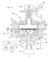
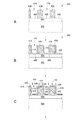
- マルチパターニングプロセス中にスペーサ層を堆積しパターニングする方法であって、
基板上に配置されたパターニングされた構造であって、その間に画定された開口部の第1の群を有するパターニングされた構造の外面上にスペーサ層を共形的に形成することと、
前記基板上に形成された前記スペーサ層の第1の部分を、前記スペーサ層の第2の部分を処理することなく、選択的に処理することと、
前記スペーサ層の処理された前記第1の部分を選択的に除去することと
を含む方法。 - 前記パターニングされた構造が、アモルファスカーボン材料、窒化ケイ素、二酸化ケイ素または炭化ケイ素を含む、請求項1に記載の方法。
- 前記スペーサ層が、ポリシリコンまたはアモルファスシリコンを含む、請求項1または2に記載の方法。
- 前記基板上にスペーサ層を共形的に形成する前に前記基板を前処理することをさらに含む、請求項1から3のいずれか一項に記載の方法。
- 前記基板を前処理することが、
不活性ガスを含む前処理混合ガスを前記基板に供給することと、
前記基板の温度をセ氏約200度からセ氏約400度の間に維持することと
をさらに含む、請求項4に記載の方法。 - 約2000ワットの上部誘導結合ソース電力および約4000ワットの側部誘導結合ソース電力を印加することをさらに含む、請求項5に記載の方法。
- 前記スペーサ層を共形的に形成することが、シリコン系ガスとN2ガスとを含む堆積混合ガスを供給することをさらに含む、請求項1から6のいずれか一項に記載の方法。
- 前記堆積混合ガスを供給することが、
前記堆積混合ガスに6500ワット未満の誘導結合ソース電力を印加することと、
前記堆積混合ガスに100ワットから約500ワットの間のRFバイアス電力を印加することと
をさらに含む、請求項7に記載の方法。 - 前記スペーサ層の前記第1の部分を選択的に処理することが、不活性ガスを含む堆積後処理混合ガスを前記基板に供給することをさらに含む、請求項1から8のいずれか一項に記載の方法。
- 前記堆積後処理混合ガスを供給することが、RFソース電力なしで250ワットから約1500ワットの間のRFバイアス電力を前記堆積後処理混合ガスに印加することをさらに含む、請求項9に記載の方法。
- 前記スペーサ層の前記第1の部分を選択的に処理することが、前記スペーサ層の側壁およびコーナー部を処理することなく前記スペーサ層の上面および底面を選択的に処理することをさらに含む、請求項1から8のいずれか一項に記載の方法。
- 前記スペーサ層の処理された前記第1の部分を選択的に除去することが、
アンモニア(NH3)ガスと三フッ化窒素(NF3)ガスとを含む選択的除去混合ガスを供給することと、
遠隔プラズマ源を前記選択的除去混合ガスに印加することと
をさらに含む、請求項1から11のいずれか一項に記載の方法。 - 前記スペーサ層の処理された前記第1の部分を選択的に除去することが、前記スペーサ層の側壁およびコーナー部を含む前記第2の部分を実質的に攻撃することなく、前記スペーサ層の上面および底面を含む前記スペーサ層の前記第1の部分を優勢にエッチングすることをさらに含む、請求項1から11のいずれか一項に記載の方法。
- 前記基板から前記パターニングされた構造を除去することと、
前記開口部の第1の群の寸法よりも小さい寸法を有する開口部の第2の群を、エッチングされた前記スペーサ層に形成することと
をさらに含む、請求項1から13のいずれか一項に記載の方法。 - 前記スペーサ層を共形的に形成することと、前記スペーサ層の前記第1の部分を選択的に処理することと、前記スペーサ層の処理された前記第1の部分を選択的に除去することとが、全て単一の処理チャンバ内で行なわれる、請求項1から14のいずれか一項に記載の方法。
Applications Claiming Priority (3)
| Application Number | Priority Date | Filing Date | Title |
|---|---|---|---|
| US14/729,932 US9484202B1 (en) | 2015-06-03 | 2015-06-03 | Apparatus and methods for spacer deposition and selective removal in an advanced patterning process |
| US14/729,932 | 2015-06-03 | ||
| PCT/US2016/033882 WO2016196073A1 (en) | 2015-06-03 | 2016-05-24 | Apparatus and methods for spacer deposition and selective removal in an advanced patterning process |
Publications (2)
| Publication Number | Publication Date |
|---|---|
| JP2018516463A JP2018516463A (ja) | 2018-06-21 |
| JP6810059B2 true JP6810059B2 (ja) | 2021-01-06 |
Family
ID=57189280
Family Applications (1)
| Application Number | Title | Priority Date | Filing Date |
|---|---|---|---|
| JP2017562685A Active JP6810059B2 (ja) | 2015-06-03 | 2016-05-24 | 先進的なパターニングプロセスにおけるスペーサ堆積および選択的除去のための装置および方法 |
Country Status (6)
| Country | Link |
|---|---|
| US (1) | US9484202B1 (ja) |
| JP (1) | JP6810059B2 (ja) |
| KR (1) | KR102483741B1 (ja) |
| CN (1) | CN107735851B (ja) |
| TW (1) | TWI627724B (ja) |
| WO (1) | WO2016196073A1 (ja) |
Families Citing this family (21)
| Publication number | Priority date | Publication date | Assignee | Title |
|---|---|---|---|---|
| WO2017210141A1 (en) * | 2016-05-29 | 2017-12-07 | Tokyo Electron Limited | Method of sidewall image transfer |
| US20170345673A1 (en) * | 2016-05-29 | 2017-11-30 | Tokyo Electron Limited | Method of selective silicon oxide etching |
| US10858727B2 (en) | 2016-08-19 | 2020-12-08 | Applied Materials, Inc. | High density, low stress amorphous carbon film, and process and equipment for its deposition |
| US10276379B2 (en) * | 2017-04-07 | 2019-04-30 | Applied Materials, Inc. | Treatment approach to improve film roughness by improving nucleation/adhesion of silicon oxide |
| WO2019022826A1 (en) * | 2017-07-24 | 2019-01-31 | Applied Materials, Inc. | PRETREATMENT APPARATUS FOR IMPROVING THE CONTINUITY OF ULTRA-THIN AMORPHOUS SILICON FILM ON SILICON OXIDE |
| US10147611B1 (en) | 2017-08-28 | 2018-12-04 | Nanya Technology Corporation | Method for preparing semiconductor structures |
| US10607852B2 (en) * | 2017-09-13 | 2020-03-31 | Tokyo Electron Limited | Selective nitride etching method for self-aligned multiple patterning |
| KR20190035036A (ko) * | 2017-09-25 | 2019-04-03 | 삼성전자주식회사 | 박막 형성 장치 및 이를 이용한 비정질 실리콘 막 형성방법 |
| US10636675B2 (en) | 2017-09-27 | 2020-04-28 | Applied Materials, Inc. | Methods of etching metal-containing layers |
| US10734228B2 (en) * | 2017-12-19 | 2020-08-04 | Tokyo Electron Limited | Manufacturing methods to apply stress engineering to self-aligned multi-patterning (SAMP) processes |
| US10910381B2 (en) * | 2018-08-01 | 2021-02-02 | Applied Materials, Inc. | Multicolor approach to DRAM STI active cut patterning |
| US11114306B2 (en) * | 2018-09-17 | 2021-09-07 | Applied Materials, Inc. | Methods for depositing dielectric material |
| US11551930B2 (en) * | 2018-12-12 | 2023-01-10 | Tokyo Electron Limited | Methods to reshape spacer profiles in self-aligned multiple patterning |
| CN111384172B (zh) * | 2018-12-29 | 2024-01-26 | 中芯国际集成电路制造(上海)有限公司 | 半导体器件及其形成方法 |
| US10629451B1 (en) * | 2019-02-01 | 2020-04-21 | American Air Liquide, Inc. | Method to improve profile control during selective etching of silicon nitride spacers |
| CN109979816A (zh) * | 2019-03-26 | 2019-07-05 | 上海华力集成电路制造有限公司 | 改善隔离侧墙形貌的方法 |
| US11355342B2 (en) * | 2019-06-13 | 2022-06-07 | Nanya Technology Corporation | Semiconductor device with reduced critical dimensions and method of manufacturing the same |
| CN112786436B (zh) * | 2019-11-06 | 2024-12-27 | 中芯国际集成电路制造(上海)有限公司 | 半导体结构及其形成方法 |
| CN113496895B (zh) * | 2020-04-01 | 2025-01-14 | 中芯国际集成电路制造(上海)有限公司 | 半导体结构的形成方法 |
| US12406855B2 (en) * | 2022-02-11 | 2025-09-02 | Nanya Technology Corporation | Method for preparing semiconductor device structure with energy removable spacers |
| TW202402387A (zh) * | 2022-04-06 | 2024-01-16 | 荷蘭商Asm Ip私人控股有限公司 | 氣體遞送總成及包括氣體遞送總成之反應器系統 |
Family Cites Families (24)
| Publication number | Priority date | Publication date | Assignee | Title |
|---|---|---|---|---|
| US6949203B2 (en) * | 1999-12-28 | 2005-09-27 | Applied Materials, Inc. | System level in-situ integrated dielectric etch process particularly useful for copper dual damascene |
| CN100451831C (zh) * | 2001-10-29 | 2009-01-14 | 旺宏电子股份有限公司 | 减小图案间隙或开口尺寸的方法 |
| US7271107B2 (en) * | 2005-02-03 | 2007-09-18 | Lam Research Corporation | Reduction of feature critical dimensions using multiple masks |
| US7807575B2 (en) * | 2006-11-29 | 2010-10-05 | Micron Technology, Inc. | Methods to reduce the critical dimension of semiconductor devices |
| CN101339361A (zh) * | 2007-06-01 | 2009-01-07 | 应用材料公司 | 利用间隔物掩模的频率加倍 |
| JP5254351B2 (ja) * | 2007-11-08 | 2013-08-07 | ラム リサーチ コーポレーション | 酸化物スペーサを使用したピッチ低減 |
| US20090286402A1 (en) * | 2008-05-13 | 2009-11-19 | Applied Materials, Inc | Method for critical dimension shrink using conformal pecvd films |
| US8232212B2 (en) * | 2008-07-11 | 2012-07-31 | Applied Materials, Inc. | Within-sequence metrology based process tuning for adaptive self-aligned double patterning |
| US8361338B2 (en) * | 2010-02-11 | 2013-01-29 | Taiwan Semiconductor Manufacturing Company, Ltd. | Hard mask removal method |
| US8728956B2 (en) * | 2010-04-15 | 2014-05-20 | Novellus Systems, Inc. | Plasma activated conformal film deposition |
| US9390909B2 (en) * | 2013-11-07 | 2016-07-12 | Novellus Systems, Inc. | Soft landing nanolaminates for advanced patterning |
| KR20120121795A (ko) * | 2011-04-27 | 2012-11-06 | 에스케이하이닉스 주식회사 | 에어 갭을 포함하는 스페이서를 구비한 반도체 소자의 제조방법 |
| US8609548B2 (en) * | 2011-06-06 | 2013-12-17 | Lam Research Corporation | Method for providing high etch rate |
| KR101835114B1 (ko) | 2011-09-07 | 2018-03-06 | 삼성전자주식회사 | 3차원 반도체 장치 및 그 제조 방법 |
| US8431461B1 (en) * | 2011-12-16 | 2013-04-30 | Lam Research Corporation | Silicon nitride dry trim without top pulldown |
| US20130189845A1 (en) * | 2012-01-19 | 2013-07-25 | Applied Materials, Inc. | Conformal amorphous carbon for spacer and spacer protection applications |
| US8980111B2 (en) | 2012-05-15 | 2015-03-17 | Tokyo Electron Limited | Sidewall image transfer method for low aspect ratio patterns |
| CN102709230B (zh) * | 2012-05-22 | 2015-05-20 | 上海华力微电子有限公司 | 一种形成半导体通孔的方法 |
| CN103779211B (zh) * | 2012-10-18 | 2017-02-01 | 中芯国际集成电路制造(上海)有限公司 | 一种半导体器件的制造方法 |
| US9362133B2 (en) * | 2012-12-14 | 2016-06-07 | Lam Research Corporation | Method for forming a mask by etching conformal film on patterned ashable hardmask |
| US20150014772A1 (en) | 2013-07-11 | 2015-01-15 | International Business Machines Corporation | Patterning fins and planar areas in silicon |
| US9318412B2 (en) | 2013-07-26 | 2016-04-19 | Nanya Technology Corporation | Method for semiconductor self-aligned patterning |
| US9159579B2 (en) | 2013-10-25 | 2015-10-13 | Taiwan Semiconductor Manufacturing Company, Ltd. | Lithography using multilayer spacer for reduced spacer footing |
| TWI531032B (zh) * | 2013-11-21 | 2016-04-21 | 力晶科技股份有限公司 | 記憶體線路結構以及其半導體線路製程 |
-
2015
- 2015-06-03 US US14/729,932 patent/US9484202B1/en active Active
-
2016
- 2016-05-24 JP JP2017562685A patent/JP6810059B2/ja active Active
- 2016-05-24 WO PCT/US2016/033882 patent/WO2016196073A1/en not_active Ceased
- 2016-05-24 KR KR1020177037639A patent/KR102483741B1/ko active Active
- 2016-05-24 CN CN201680031800.7A patent/CN107735851B/zh active Active
- 2016-05-25 TW TW105116333A patent/TWI627724B/zh active
Also Published As
| Publication number | Publication date |
|---|---|
| TWI627724B (zh) | 2018-06-21 |
| CN107735851A (zh) | 2018-02-23 |
| US9484202B1 (en) | 2016-11-01 |
| KR102483741B1 (ko) | 2023-01-03 |
| CN107735851B (zh) | 2021-11-05 |
| JP2018516463A (ja) | 2018-06-21 |
| TW201705428A (zh) | 2017-02-01 |
| WO2016196073A1 (en) | 2016-12-08 |
| KR20180005265A (ko) | 2018-01-15 |
Similar Documents
| Publication | Publication Date | Title |
|---|---|---|
| JP6810059B2 (ja) | 先進的なパターニングプロセスにおけるスペーサ堆積および選択的除去のための装置および方法 | |
| JP6787868B2 (ja) | 低k及びその他の誘電体膜をエッチングするための処理チャンバ | |
| JP7176106B2 (ja) | 誘電体材料の堆積方法 | |
| KR102283949B1 (ko) | 주기적 에칭 프로세스를 이용하여 에칭 스톱 층을 에칭하기 위한 방법들 | |
| US9543163B2 (en) | Methods for forming features in a material layer utilizing a combination of a main etching and a cyclical etching process | |
| US9640385B2 (en) | Gate electrode material residual removal process | |
| US9741566B2 (en) | Methods for manufacturing a spacer with desired profile in an advanced patterning process | |
| TWI817066B (zh) | 用於蝕刻用於半導體應用的材料層的方法 |
Legal Events
| Date | Code | Title | Description |
|---|---|---|---|
| A621 | Written request for application examination |
Free format text: JAPANESE INTERMEDIATE CODE: A621 Effective date: 20190517 |
|
| A131 | Notification of reasons for refusal |
Free format text: JAPANESE INTERMEDIATE CODE: A131 Effective date: 20200616 |
|
| A521 | Request for written amendment filed |
Free format text: JAPANESE INTERMEDIATE CODE: A523 Effective date: 20200909 |
|
| TRDD | Decision of grant or rejection written | ||
| A01 | Written decision to grant a patent or to grant a registration (utility model) |
Free format text: JAPANESE INTERMEDIATE CODE: A01 Effective date: 20201110 |
|
| A61 | First payment of annual fees (during grant procedure) |
Free format text: JAPANESE INTERMEDIATE CODE: A61 Effective date: 20201210 |
|
| R150 | Certificate of patent or registration of utility model |
Ref document number: 6810059 Country of ref document: JP Free format text: JAPANESE INTERMEDIATE CODE: R150 |
|
| R250 | Receipt of annual fees |
Free format text: JAPANESE INTERMEDIATE CODE: R250 |
|
| R250 | Receipt of annual fees |
Free format text: JAPANESE INTERMEDIATE CODE: R250 |