JP6830772B2 - Laminated film manufacturing equipment and laminated film manufacturing method - Google Patents
Laminated film manufacturing equipment and laminated film manufacturing method Download PDFInfo
- Publication number
- JP6830772B2 JP6830772B2 JP2016153361A JP2016153361A JP6830772B2 JP 6830772 B2 JP6830772 B2 JP 6830772B2 JP 2016153361 A JP2016153361 A JP 2016153361A JP 2016153361 A JP2016153361 A JP 2016153361A JP 6830772 B2 JP6830772 B2 JP 6830772B2
- Authority
- JP
- Japan
- Prior art keywords
- substrate
- processed
- chamber
- transport
- transfer machine
- Prior art date
- Legal status (The legal status is an assumption and is not a legal conclusion. Google has not performed a legal analysis and makes no representation as to the accuracy of the status listed.)
- Active
Links
Images


Classifications
-
- H—ELECTRICITY
- H10—SEMICONDUCTOR DEVICES; ELECTRIC SOLID-STATE DEVICES NOT OTHERWISE PROVIDED FOR
- H10K—ORGANIC ELECTRIC SOLID-STATE DEVICES
- H10K71/00—Manufacture or treatment specially adapted for the organic devices covered by this subclass
- H10K71/10—Deposition of organic active material
- H10K71/16—Deposition of organic active material using physical vapour deposition [PVD], e.g. vacuum deposition or sputtering
-
- C—CHEMISTRY; METALLURGY
- C23—COATING METALLIC MATERIAL; COATING MATERIAL WITH METALLIC MATERIAL; CHEMICAL SURFACE TREATMENT; DIFFUSION TREATMENT OF METALLIC MATERIAL; COATING BY VACUUM EVAPORATION, BY SPUTTERING, BY ION IMPLANTATION OR BY CHEMICAL VAPOUR DEPOSITION, IN GENERAL; INHIBITING CORROSION OF METALLIC MATERIAL OR INCRUSTATION IN GENERAL
- C23C—COATING METALLIC MATERIAL; COATING MATERIAL WITH METALLIC MATERIAL; SURFACE TREATMENT OF METALLIC MATERIAL BY DIFFUSION INTO THE SURFACE, BY CHEMICAL CONVERSION OR SUBSTITUTION; COATING BY VACUUM EVAPORATION, BY SPUTTERING, BY ION IMPLANTATION OR BY CHEMICAL VAPOUR DEPOSITION, IN GENERAL
- C23C14/00—Coating by vacuum evaporation, by sputtering or by ion implantation of the coating forming material
- C23C14/22—Coating by vacuum evaporation, by sputtering or by ion implantation of the coating forming material characterised by the process of coating
- C23C14/56—Apparatus specially adapted for continuous coating; Arrangements for maintaining the vacuum, e.g. vacuum locks
- C23C14/568—Transferring the substrates through a series of coating stations
-
- C—CHEMISTRY; METALLURGY
- C23—COATING METALLIC MATERIAL; COATING MATERIAL WITH METALLIC MATERIAL; CHEMICAL SURFACE TREATMENT; DIFFUSION TREATMENT OF METALLIC MATERIAL; COATING BY VACUUM EVAPORATION, BY SPUTTERING, BY ION IMPLANTATION OR BY CHEMICAL VAPOUR DEPOSITION, IN GENERAL; INHIBITING CORROSION OF METALLIC MATERIAL OR INCRUSTATION IN GENERAL
- C23C—COATING METALLIC MATERIAL; COATING MATERIAL WITH METALLIC MATERIAL; SURFACE TREATMENT OF METALLIC MATERIAL BY DIFFUSION INTO THE SURFACE, BY CHEMICAL CONVERSION OR SUBSTITUTION; COATING BY VACUUM EVAPORATION, BY SPUTTERING, BY ION IMPLANTATION OR BY CHEMICAL VAPOUR DEPOSITION, IN GENERAL
- C23C14/00—Coating by vacuum evaporation, by sputtering or by ion implantation of the coating forming material
- C23C14/06—Coating by vacuum evaporation, by sputtering or by ion implantation of the coating forming material characterised by the coating material
- C23C14/12—Organic material
-
- C—CHEMISTRY; METALLURGY
- C23—COATING METALLIC MATERIAL; COATING MATERIAL WITH METALLIC MATERIAL; CHEMICAL SURFACE TREATMENT; DIFFUSION TREATMENT OF METALLIC MATERIAL; COATING BY VACUUM EVAPORATION, BY SPUTTERING, BY ION IMPLANTATION OR BY CHEMICAL VAPOUR DEPOSITION, IN GENERAL; INHIBITING CORROSION OF METALLIC MATERIAL OR INCRUSTATION IN GENERAL
- C23C—COATING METALLIC MATERIAL; COATING MATERIAL WITH METALLIC MATERIAL; SURFACE TREATMENT OF METALLIC MATERIAL BY DIFFUSION INTO THE SURFACE, BY CHEMICAL CONVERSION OR SUBSTITUTION; COATING BY VACUUM EVAPORATION, BY SPUTTERING, BY ION IMPLANTATION OR BY CHEMICAL VAPOUR DEPOSITION, IN GENERAL
- C23C14/00—Coating by vacuum evaporation, by sputtering or by ion implantation of the coating forming material
- C23C14/22—Coating by vacuum evaporation, by sputtering or by ion implantation of the coating forming material characterised by the process of coating
- C23C14/24—Vacuum evaporation
-
- H—ELECTRICITY
- H10—SEMICONDUCTOR DEVICES; ELECTRIC SOLID-STATE DEVICES NOT OTHERWISE PROVIDED FOR
- H10K—ORGANIC ELECTRIC SOLID-STATE DEVICES
- H10K59/00—Integrated devices, or assemblies of multiple devices, comprising at least one organic light-emitting element covered by group H10K50/00
- H10K59/10—OLED displays
- H10K59/12—Active-matrix OLED [AMOLED] displays
- H10K59/122—Pixel-defining structures or layers, e.g. banks
-
- H—ELECTRICITY
- H10—SEMICONDUCTOR DEVICES; ELECTRIC SOLID-STATE DEVICES NOT OTHERWISE PROVIDED FOR
- H10K—ORGANIC ELECTRIC SOLID-STATE DEVICES
- H10K71/00—Manufacture or treatment specially adapted for the organic devices covered by this subclass
-
- H—ELECTRICITY
- H10—SEMICONDUCTOR DEVICES; ELECTRIC SOLID-STATE DEVICES NOT OTHERWISE PROVIDED FOR
- H10K—ORGANIC ELECTRIC SOLID-STATE DEVICES
- H10K71/00—Manufacture or treatment specially adapted for the organic devices covered by this subclass
- H10K71/60—Forming conductive regions or layers, e.g. electrodes
-
- H—ELECTRICITY
- H10—SEMICONDUCTOR DEVICES; ELECTRIC SOLID-STATE DEVICES NOT OTHERWISE PROVIDED FOR
- H10P—GENERIC PROCESSES OR APPARATUS FOR THE MANUFACTURE OR TREATMENT OF DEVICES COVERED BY CLASS H10
- H10P72/00—Handling or holding of wafers, substrates or devices during manufacture or treatment thereof
- H10P72/04—Apparatus for manufacture or treatment
- H10P72/0451—Apparatus for manufacturing or treating in a plurality of work-stations
- H10P72/0452—Apparatus for manufacturing or treating in a plurality of work-stations characterised by the layout of the process chambers
- H10P72/0456—Apparatus for manufacturing or treating in a plurality of work-stations characterised by the layout of the process chambers in-line arrangement
-
- H—ELECTRICITY
- H10—SEMICONDUCTOR DEVICES; ELECTRIC SOLID-STATE DEVICES NOT OTHERWISE PROVIDED FOR
- H10P—GENERIC PROCESSES OR APPARATUS FOR THE MANUFACTURE OR TREATMENT OF DEVICES COVERED BY CLASS H10
- H10P72/00—Handling or holding of wafers, substrates or devices during manufacture or treatment thereof
- H10P72/04—Apparatus for manufacture or treatment
- H10P72/0451—Apparatus for manufacturing or treating in a plurality of work-stations
- H10P72/0461—Apparatus for manufacturing or treating in a plurality of work-stations characterised by the presence of two or more transfer chambers
-
- H—ELECTRICITY
- H10—SEMICONDUCTOR DEVICES; ELECTRIC SOLID-STATE DEVICES NOT OTHERWISE PROVIDED FOR
- H10P—GENERIC PROCESSES OR APPARATUS FOR THE MANUFACTURE OR TREATMENT OF DEVICES COVERED BY CLASS H10
- H10P72/00—Handling or holding of wafers, substrates or devices during manufacture or treatment thereof
- H10P72/30—Handling or holding of wafers, substrates or devices during manufacture or treatment thereof for conveying, e.g. between different workstations
- H10P72/33—Handling or holding of wafers, substrates or devices during manufacture or treatment thereof for conveying, e.g. between different workstations into and out of processing chamber
- H10P72/3304—Handling or holding of wafers, substrates or devices during manufacture or treatment thereof for conveying, e.g. between different workstations into and out of processing chamber characterised by movements or sequence of movements of transfer devices
-
- H—ELECTRICITY
- H10—SEMICONDUCTOR DEVICES; ELECTRIC SOLID-STATE DEVICES NOT OTHERWISE PROVIDED FOR
- H10P—GENERIC PROCESSES OR APPARATUS FOR THE MANUFACTURE OR TREATMENT OF DEVICES COVERED BY CLASS H10
- H10P72/00—Handling or holding of wafers, substrates or devices during manufacture or treatment thereof
- H10P72/30—Handling or holding of wafers, substrates or devices during manufacture or treatment thereof for conveying, e.g. between different workstations
- H10P72/33—Handling or holding of wafers, substrates or devices during manufacture or treatment thereof for conveying, e.g. between different workstations into and out of processing chamber
- H10P72/3306—Horizontal transfer of a single workpiece
-
- H—ELECTRICITY
- H10—SEMICONDUCTOR DEVICES; ELECTRIC SOLID-STATE DEVICES NOT OTHERWISE PROVIDED FOR
- H10P—GENERIC PROCESSES OR APPARATUS FOR THE MANUFACTURE OR TREATMENT OF DEVICES COVERED BY CLASS H10
- H10P72/00—Handling or holding of wafers, substrates or devices during manufacture or treatment thereof
- H10P72/30—Handling or holding of wafers, substrates or devices during manufacture or treatment thereof for conveying, e.g. between different workstations
- H10P72/33—Handling or holding of wafers, substrates or devices during manufacture or treatment thereof for conveying, e.g. between different workstations into and out of processing chamber
- H10P72/3308—Vertical transfer of a single workpiece
-
- H—ELECTRICITY
- H10—SEMICONDUCTOR DEVICES; ELECTRIC SOLID-STATE DEVICES NOT OTHERWISE PROVIDED FOR
- H10K—ORGANIC ELECTRIC SOLID-STATE DEVICES
- H10K71/00—Manufacture or treatment specially adapted for the organic devices covered by this subclass
- H10K71/10—Deposition of organic active material
- H10K71/16—Deposition of organic active material using physical vapour deposition [PVD], e.g. vacuum deposition or sputtering
- H10K71/166—Deposition of organic active material using physical vapour deposition [PVD], e.g. vacuum deposition or sputtering using selective deposition, e.g. using a mask
Landscapes
- Chemical & Material Sciences (AREA)
- Engineering & Computer Science (AREA)
- Manufacturing & Machinery (AREA)
- Chemical Kinetics & Catalysis (AREA)
- Materials Engineering (AREA)
- Mechanical Engineering (AREA)
- Metallurgy (AREA)
- Organic Chemistry (AREA)
- Microelectronics & Electronic Packaging (AREA)
- Electroluminescent Light Sources (AREA)
- Physical Vapour Deposition (AREA)
- Chemical Vapour Deposition (AREA)
Description
本発明は、発光素子の製造装置及びその製造方法に関する。特に、表示装置に有機EL素子を形成する有機層および電極層を形成するための製造装置及びその製造方法に関する。 The present invention relates to an apparatus for manufacturing a light emitting element and a method for manufacturing the same. In particular, the present invention relates to a manufacturing apparatus for forming an organic layer and an electrode layer for forming an organic EL element in a display device, and a manufacturing method thereof.
近年、表示部に有機エレクトロルミネッセンス素子(有機EL素子)を用いた表示装置が、スマートフォン等の携帯情報端末を始め、様々な電子デバイスに広く用いられている。有機EL素子は、一対の電極の間に、各機能を有する有機層を積層挟持した構造を有し、その製造は、一方の電極が形成された基板上に、有機層を蒸着法又は塗布法等によって順次形成し、他方の電極をスパッタリング又は塗布法等によって形成することで行われる。 In recent years, display devices using an organic electroluminescence element (organic EL element) for the display unit have been widely used in various electronic devices including portable information terminals such as smartphones. The organic EL element has a structure in which an organic layer having each function is laminated and sandwiched between a pair of electrodes, and the production thereof is performed by a vapor deposition method or a coating method of an organic layer on a substrate on which one electrode is formed. It is performed by sequentially forming the other electrode by sputtering, coating method, or the like.
代表的な有機EL素子の有機層の構造としては、正孔注入層\正孔輸送層\発光層\電子輸送層\電子注入層といった積層構造が挙げられるが、これらを含め、有機EL素子を構成する積層を順次好適に形成するための製造装置が提案されている(例えば、特許文献1参照)。 Examples of the structure of the organic layer of a typical organic EL device include a laminated structure such as a hole injection layer \ a hole transport layer \ a light emitting layer \ an electron transport layer \ an electron injection layer. A manufacturing apparatus for sequentially preferably forming the constituent laminates has been proposed (see, for example, Patent Document 1).
有機EL素子は、一対の電極間に挟持された有機層の材料、及び積層により構成されるが、要求する特性に応じてその構造は大きく異なる。このため、従来の有機EL素子とは異なる材料、及び積層構造を有する素子が提案されるに従い、それに合わせた製造装置の構築が必要となる。例えば特許文献1に記載の製造装置等においては、複数の処理室が接続された搬送室が、受渡室を介して直列に接続されているが、このような構成の場合、途中で積層構造を変更、あるいは新たな層を追加するには、一度配置した装置群の一部を分解して再配置する、あるいは新たな搬送室を追加接続するといった大規模な改修を必要とする。また、各処理はそれぞれの処理時間が異なるため、ある一工程では処理能力が高く、他の一工程では処理能力が低いといった差が生ずるが、搬送室が直列に接続されている場合、処理能力の低い工程がボトルネックとなり、全体のスループットを律速してしまうといった問題がある。 The organic EL element is composed of an organic layer material sandwiched between a pair of electrodes and a laminate, but the structure thereof varies greatly depending on the required characteristics. Therefore, as a material different from the conventional organic EL element and an element having a laminated structure are proposed, it is necessary to construct a manufacturing apparatus according to the material. For example, in the manufacturing apparatus or the like described in Patent Document 1, the transport chambers to which a plurality of processing chambers are connected are connected in series via the delivery chamber, but in the case of such a configuration, a laminated structure is formed in the middle. In order to change or add a new layer, a large-scale renovation is required, such as disassembling and relocating a part of the equipment group once placed, or adding a new transport chamber. In addition, since each process has a different processing time, there is a difference that the processing capacity is high in one process and low in the other process, but when the transport chambers are connected in series, the processing capacity is high. There is a problem that the low process becomes a bottleneck and limits the overall throughput.
本発明は、上記に鑑み、各工程の処理能力に応じた最適な装置の構成を可能とし、かつ積層構造の変更や新たな層の追加等に伴う工程変更にも柔軟に対応することのできる発光素子の製造装置を提供することを課題の一とする。 In view of the above, the present invention makes it possible to configure an optimum apparatus according to the processing capacity of each process, and can flexibly respond to process changes due to changes in the laminated structure, addition of new layers, and the like. One of the issues is to provide a manufacturing apparatus for a light emitting element.
本発明の一態様である積層膜の製造装置は、第1受渡室を介して接続された、第1及び第2移載機を有する主搬送路と、第1又は第2移載機に接続された第2受渡室、及び第2受渡室に接続された搬送室とを有し、主搬送路と交差する方向に延在する副搬送路と、搬送室に接続された、複数の第1処理室と、を有し、主搬送路は、被処理基板を水平な状態で搬送されるように構成され、複数の第1処理室の一は、処理中に被処理基板を垂直な状態で保持するように構成されたことを特徴とする。 The laminated film manufacturing apparatus according to one aspect of the present invention is connected to a main transport path having first and second transfer machines, which is connected via a first delivery chamber, and to a first or second transfer machine. A plurality of first delivery chambers connected to the transport chamber and a secondary transport passage extending in a direction intersecting the main transport passage, which has a second delivery chamber and a transport chamber connected to the second delivery chamber. It has a processing chamber, and the main transport path is configured to transport the substrate to be processed in a horizontal state, and one of the plurality of first processing chambers has a processing substrate in a vertical state during processing. It is characterized by being configured to hold.
本発明の他の一態様である積層膜の製造装置は、第1受渡室を介して接続された、第1及び第2移載機を有する主搬送路と、第1移載機に接続された第2受渡室、及び第2受渡室に接続された第1搬送室とを有し、主搬送路と交差する方向に延在する第1副搬送路と、第2移載機に接続された第3受渡室、及び第3受渡室に接続された第2搬送室とを有し、主搬送路と交差する方向に延在する第2副搬送路と、第1搬送室に接続された複数の第1処理室と、第2搬送室に接続された複数の第2処理室と、を有し、主搬送路は、被処理基板を水平な状態で搬送するように構成され、複数の第1処理室の一は、処理中に被処理基板を垂直な状態で保持するように構成され、複数の第2処理室の一は、処理中に被処理基板を水平な状態で保持するように構成されたことを特徴とする。 The apparatus for producing a laminated film, which is another aspect of the present invention, is connected to a main transport path having first and second transfer machines, which is connected via a first delivery chamber, and to the first transfer machine. It has a second delivery chamber and a first transport chamber connected to the second delivery chamber, and is connected to a first sub-transport passage extending in a direction intersecting the main transport passage and a second transfer machine. It has a third delivery chamber and a second transport chamber connected to the third delivery chamber, and is connected to a second transport passage extending in a direction intersecting the main transport passage and a first transport chamber. It has a plurality of first processing chambers and a plurality of second processing chambers connected to the second transport chamber, and the main transport path is configured to transport the substrate to be processed in a horizontal state. One of the first processing chambers is configured to hold the substrate to be processed in a vertical state during processing, and one of the plurality of second processing chambers holds the substrate to be processed in a horizontal state during processing. It is characterized by being configured in.
本発明の一態様である積層膜の製造方法は、第1受渡室を介して接続された、第1及び第2移載機を有する主搬送路と、第1又は第2移載機に接続された第2受渡室、及び第2受渡室に接続された搬送室とを有し、主搬送路と交差する方向に延在する副搬送路と、搬送室に接続された、複数の第1処理室と、を有する製造装置を用いた積層膜の製造方法であって、絶縁表面上に、画素電極と、画素電極の端部を覆うと共に、画素電極の上面の一部を露出するバンクと、を有する被処理基板を用意し、被処理基板を、製造装置の主搬送路上に設けられた第1移載機に搬入し、被処理基板を、第1移載機から、第2受渡室を介して搬送室に搬入し、被処理基板を、搬送室から複数の第1処理室の一に搬入し、被処理基板を水平な状態に保持して、画素電極及びバンク上に第1有機層を形成し、被処理基板を、複数の第1処理室の一から搬送室に戻し、被処理基板を、搬送室から複数の第1処理室の他の一に搬入し、被処理基板を垂直な状態に保持して、第1有機層上の、画素電極に重畳する領域に第2有機層を形成し、被処理基板を、複数の第1処理室の他の一から搬送室に戻し、被処理基板を、搬送室から、第2受渡室を介して第1移載機に戻す工程を含み、被処理基板が、搬送室から複数の第1処理室の他の一に搬入されるまでの間に、水平な状態から垂直な状態に転回される工程を含む。 The method for producing a laminated film, which is one aspect of the present invention, is connected to a main transport path having first and second transfer machines, which is connected via a first delivery chamber, and a first or second transfer machine. A plurality of first delivery chambers connected to the transport chamber and a secondary transport passage extending in a direction intersecting the main transport passage, which has a second delivery chamber and a transport chamber connected to the second delivery chamber. A method for manufacturing a laminated film using a manufacturing apparatus having a processing chamber, which comprises a pixel electrode and a bank that covers an end portion of the pixel electrode and exposes a part of the upper surface of the pixel electrode on an insulating surface. The substrate to be processed is prepared, the substrate to be processed is carried into the first transfer machine provided on the main transport path of the manufacturing apparatus, and the substrate to be processed is transferred from the first transfer machine to the second delivery chamber. The substrate to be processed is carried from the transport chamber into one of a plurality of first processing chambers, and the substrate to be processed is held in a horizontal state, and the first organic is carried on the pixel electrode and the bank. A layer is formed, the substrate to be processed is returned from one of the plurality of first processing chambers to the transport chamber, the substrate to be processed is carried from the transport chamber to the other one of the plurality of first treatment chambers, and the substrate to be processed is carried. The second organic layer is formed in the region on the first organic layer that overlaps with the pixel electrodes while being held in a vertical state, and the substrate to be processed is returned from the other one of the plurality of first processing chambers to the transport chamber. , The process of returning the substrate to be processed from the transfer chamber to the first transfer machine via the second delivery chamber is included, and the substrate to be processed is carried from the transfer chamber to another one of the plurality of first processing chambers. In the meantime, it includes a step of turning from a horizontal state to a vertical state.
本発明の他の一態様である積層膜の製造方法は、第1受渡室を介して接続された、第1及び第2移載機を有する主搬送路と、第1移載機に接続された第2受渡室、及び第2受渡室に接続された第1搬送室とを有し、主搬送路と交差する方向に延在する第1副搬送路と、第2移載機に接続された第3受渡室、及び第3受渡室に接続された第2搬送室とを有し、主搬送路と交差する方向に延在する第2副搬送路と、第1搬送室に接続された複数の第1処理室と、第2搬送室に接続された複数の第2処理室と、を有する製造装置を用いた積層膜の製造方法であって、絶縁表面上に、画素電極と、画素電極の端部を覆うと共に、画素電極の上面の一部を露出するバンクと、を有する被処理基板を用意し、被処理基板を、製造装置の主搬送路上に設けられた第1移載機に搬入し、被処理基板を、第1移載機から、第2受渡室を介して第1搬送室に搬入し、被処理基板を、第1搬送室から複数の第1処理室の一に搬入し、被処理基板を水平な状態に保持して、画素電極及びバンク上に第1有機層を形成し、被処理基板を、複数の第1処理室の一から第1搬送室に戻し、被処理基板を、第1搬送室から、第2受渡室を介して第1移載機に戻し、被処理基板を、第1移載機から、第1受渡室を介して第2移載機に搬入し、被処理基板を、第2移載機から、第3受渡室を介して第2搬送室に搬入し、被処理基板を、第2搬送室から複数の第2処理室の一に搬入し、被処理基板を垂直な状態に保持して、第1有機層上の、画素電極に重畳する領域に第2有機層を形成し、被処理基板を、第2処理室の一から第2搬送室に戻し、被処理基板を、第2搬送室から、第3受渡室を介して第2移載機に戻す工程を含み、被処理基板が、第2移載機から第2搬送室に搬入されるまでの間、又は第2搬送室から複数の第2処理室の一に搬入されるまでの間に、水平な状態から垂直な状態に転回される工程を含む。 The method for producing a laminated film, which is another aspect of the present invention, is connected to a main transport path having first and second transfer machines, which is connected via a first delivery chamber, and to the first transfer machine. It has a second delivery chamber and a first transport chamber connected to the second delivery chamber, and is connected to a first sub-transport passage extending in a direction intersecting the main transport passage and a second transfer machine. It has a third delivery chamber and a second transport chamber connected to the third delivery chamber, and is connected to a second transport passage extending in a direction intersecting the main transport passage and a first transport chamber. A method of manufacturing a laminated film using a manufacturing apparatus having a plurality of first treatment chambers and a plurality of second treatment chambers connected to a second transport chamber, wherein a pixel electrode and a pixel are formed on an insulating surface. A first transfer machine provided with a bank to cover the end of the electrode and expose a part of the upper surface of the pixel electrode, and to prepare the substrate to be processed on the main transport path of the manufacturing apparatus. The substrate to be processed is carried from the first transfer machine into the first transfer chamber via the second delivery chamber, and the substrate to be processed is transferred from the first transfer chamber to one of a plurality of first processing chambers. The substrate to be processed is carried in, the substrate to be processed is held in a horizontal state, a first organic layer is formed on the pixel electrodes and the bank, and the substrate to be processed is returned from one of the plurality of first processing chambers to the first transport chamber. The substrate to be processed is returned from the first transfer chamber to the first transfer machine via the second delivery chamber, and the substrate to be processed is returned from the first transfer machine to the second transfer machine via the first delivery chamber. The substrate to be processed is carried from the second transfer machine into the second transfer chamber via the third delivery chamber, and the substrate to be processed is transferred from the second transfer chamber to one of a plurality of second processing chambers. The substrate to be processed is carried in, the substrate to be processed is held in a vertical state, the second organic layer is formed in the region on the first organic layer superimposing on the pixel electrodes, and the substrate to be processed is transferred from the first to the first in the second processing chamber. 2 The process of returning the substrate to the transfer chamber and returning the substrate to be processed from the second transfer chamber to the second transfer machine via the third delivery chamber is included, and the substrate to be processed is transferred from the second transfer machine to the second transfer chamber. It includes a step of turning from a horizontal state to a vertical state until it is carried into the container or from the second transport chamber to one of the plurality of second processing chambers.
以下に、本発明の実施の形態の各々について、図面を参照しつつ説明する。図面は、説明をより明確にするため、実際の態様に比べ、各部の幅、厚さ、形状、大小関係等について模式的に表される場合があるが、特にそれらについての断りが無い限りは、これらはあくまで一例であって、本発明の解釈を限定するものではない。また、本明細書と各図において、既出の図に関して前述したものと同様の要素には、同一の符号を付して詳細な説明を適宜省略する場合がある。 Each of the embodiments of the present invention will be described below with reference to the drawings. In order to clarify the explanation, the drawings may schematically show the width, thickness, shape, size relationship, etc. of each part as compared with the actual mode, but unless otherwise specified. , These are merely examples and do not limit the interpretation of the present invention. Further, in the present specification and each figure, the same elements as those described above with respect to the above-mentioned figures may be designated by the same reference numerals and detailed description thereof may be omitted as appropriate.
また、本発明において、ある構造体の「上に」他の構造体を配置する態様を表現するにあたり、単に「上に」と表記する場合、特に断りの無い限りは、ある構造体に接するように、直上に他の構造体を配置する場合と、ある構造体の上方に、さらに他の構造体を介して他の構造体を配置する場合との両方を含むものとする。 Further, in the present invention, when expressing the mode of arranging another structure "on" a certain structure, when it is simply described as "on", it is in contact with a certain structure unless otherwise specified. It is assumed that both the case where another structure is arranged directly above the one structure and the case where another structure is arranged above the one structure and further via the other structure are included.
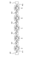
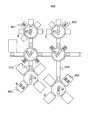
図1は、本発明の一実施形態である発光素子の製造装置100の構成例を示したものである。図1において、移載機101〜103、および搬送コンベア(受渡室)111〜113で構成される部分が主搬送路であり、移載機101〜103の各々から、主搬送路に交差する方向に、搬送コンベア131〜135を介して、処理装置A〜Eが枝状に接続されている。110は基板投入取出口であり、例えば基板ストッカ(図示せず)等と接続される。搬送コンベア111〜113、及び131〜135は、隣接する移載機の間、又は移載機と処理装置A〜Eの搬送室191〜195との間で被処理基板の受け渡しを行うものである。図1においては、主搬送路は直線状となっているが、特に限定するものではなく、この例においては主搬送路を構成する移載機101〜103、及び搬送コンベア111〜113が一筆書き線状に接続されていれば良い。
FIG. 1 shows a configuration example of a light emitting
移載機101は複数のポートを有し、ポートを介して搬送コンベア111、112、131、134が接続される。移載機101は、搬送アーム161を有し、搬送コンベア111、112、131、134と被処理基板の授受を行う。さらに、移載機101には一つ、あるいは複数のバッファ162が接続されていても良い。バッファ162は、装置投入待ちの被処理基板を一時的に退避させるものである。各処理装置A〜Eの処理能力が異なる場合、主搬送路上で被処理基板が滞留して、搬送順が前後する被処理基板がお互いを邪魔しないようにすることができる。図1においては、移載機101には2室のバッファ162が接続されているが、バッファ162は各移載機で必要な台数だけ接続されれば良く、例えば空きポート163があっても良い。
The
処理装置Aは、搬送アーム152を有する搬送室191に、各処理を行うチャンバ(処理室)151が複数接続されるように構成される。搬送室191と各チャンバ151は、ポートを介して接続される。各ポートは、ロードロック扉153を有する。ロードロック扉153は、装置の各部を必要に応じて真空又は特定雰囲気とするための気密性を備えており、ロードロック扉153の内側で連続する空間を、ロードロック扉153の外側の空間と遮断するロードロック機構を有する。図1においては、搬送室191は8箇所のポートを有し、うち1箇所を搬送コンベア131との接続で占有するため、最大7室のチャンバ151を接続することが可能である。チャンバ151は各工程で必要な台数だけ接続されれば良く、例えば空きポート154があっても良い。他の処理装置B〜Eについても同様である。
The processing device A is configured such that a plurality of chambers (processing chambers) 151 for performing each processing are connected to a
また、搬送コンベア111〜113、131〜135は、図1では基板が内部を移動するコンベア構造を有しているが、それぞれの移載機の間、又は移載機と処理装置との間の距離がそれほど長くなく、アーム161の作動範囲内で被処理基板の受け渡しが可能であるのならば、単に被処理基板を設置するステージが設けられているだけでも良い。
Further, although the
本発明の発光素子の製造装置においては、移載機101〜103、主搬送路に設けられた搬送コンベア111〜113、及び枝状に設けられた搬送コンベア131〜135で接続された領域は、真空状態を保っている。このため、複数の処理装置間を被処理基板が行き来する場合にも、被処理基板は工程途中で大気曝露されない。
In the light emitting element manufacturing apparatus of the present invention, the regions connected by the
図2に、処理工程の一例を示す。矢印は、発光素子の製造装置100内での、被処理基板の進行ルートを簡単に示している。基板投入取出口110より、被処理基板が、搬送コンベア111を介して移載機101に送られる。移載機101は、搬送コンベア131を介して、最初の処理を行う処理装置Aの搬送室191に被処理基板を投入する。処理装置A内では、搬送室191と各処理室151との間で被処理基板の受け渡しが行われ、それぞれの処理を行う。処理装置Aで全ての工程が完了すると、移載機101は搬送コンベア131から被処理基板を受け取り、搬送コンベア134に受け渡す。
FIG. 2 shows an example of the processing process. The arrow simply indicates the traveling route of the substrate to be processed in the light emitting
以後、処理装置B、C、D、E内で、順次処理が実行され、全ての処理装置での工程が完了した被処理基板は、再び基板投入取出口110に戻る。
After that, the processing is sequentially executed in the processing devices B, C, D, and E, and the substrate to be processed that has completed the steps in all the processing devices returns to the substrate loading / unloading
本発明の発光素子の製造装置の主たる特徴の一として、各処理装置A〜Eは、搬送コンベア131〜135を介して、主搬送路から枝状に接続されている点が挙げられる。例えば図2に示したように、処理装置A→B→C→D→Eのように、順次処理を行うのみならず、例えば積層構造の変更によって、使用する処理装置の順番がA→E→C→D→Bなどと変わっても、各処理装置の接続を変更せずに対応が可能である。
One of the main features of the light emitting element manufacturing apparatus of the present invention is that the processing apparatus A to E are connected in a branch shape from the main transport path via the
また、各処理装置に接続されたチャンバにおける工程は必ずしも連続しているとは限らないし、同一チャンバでの処理が、異なる工程で複数含まれる場合もある。このような場合も、被処理基板は主搬送路の往復を容易に行うことができる。 Further, the processes in the chambers connected to each processing device are not always continuous, and a plurality of processes in the same chamber may be included in different processes. Even in such a case, the substrate to be processed can easily reciprocate in the main transport path.
仮に、使用する処理装置の順番が複雑になったとしても、各移載機が有しているバッファ162によって、被処理基板の退避、すれ違いは容易に行うことができる。製造装置100内に複数の被処理基板が投入されていても同様である。
Even if the order of the processing devices to be used becomes complicated, the
移載機102の空きポート164や、移載機103の空きポート165には、将来的な拡張の余地がある。例えば、新たに処理装置170を接続したり(図1参照)、さらに搬送コンベアを接続して工程数を拡大したりすることが可能である。
There is room for future expansion in the
本発明の発光素子の製造装置100においては、このような拡張に対する柔軟性を有する。例えば空きポート164に接続する新たな処理装置170内で行われる処理は、他の処理装置で行われる処理の間に行われるものであっても良い。例えば、処理装置A→B→C→D→Eの間に、新たな処理装置Fを追加し、工程をA→F→B→C→D→Eと組み替える必要があったとしても、空きポート164を利用して処理装置Fを追加するのみで良い。他の処理装置A〜Eや、移載機101〜103等、既存の設備については移設の必要がない。
The light emitting
また、各処理装置で実施される工程は、その全てが同等の処理時間を有するとは限らず、ある工程が他の工程に比べてより長い処理時間を要することは珍しくない。長い処理時間を要する処理装置がボトルネックとなり、発光素子の製造装置全体のスループットを低下させてしまう。このような場合、空きポート164を利用して、長い処理時間を要する処理装置を並列に増設しても良い。複数の被処理基板のそれぞれを並列処理向けに振り分け、各部のバッファ162を用いることで、単機の処理装置で行う工程と、複数機の処理装置で並列で行う工程との間を適切に接続することができる。
In addition, not all of the steps performed by each processing apparatus have the same processing time, and it is not uncommon for a certain process to require a longer processing time than another process. A processing device that requires a long processing time becomes a bottleneck, and the throughput of the entire light emitting element manufacturing device is reduced. In such a case, processing devices that require a long processing time may be added in parallel by using the
例えば有機EL素子の形成には、複数の有機層の各々を別工程で純度良く成膜することが必要であり、かつその成膜環境は真空又は減圧、もしくは特定の雰囲気下であるため、多数の処理室が必要である。従って製造装置の規模が大きくなり、クリーンルームの形状、床面積に対してレイアウトが簡単でない場合がある。本発明の発光素子の製造装置100は、主搬送路上に、移載機を複数並べることで、枝状に接続される処理装置の配置自由度を高くできるため、前述の問題を適切に解決できる。
For example, in order to form an organic EL element, it is necessary to form a film of each of a plurality of organic layers with high purity in a separate process, and the film forming environment is vacuum, reduced pressure, or a specific atmosphere. Processing room is required. Therefore, the scale of the manufacturing equipment becomes large, and the layout may not be easy with respect to the shape and floor area of the clean room. In the light emitting
さらに、装置のレイアウト形状が著しく限定されるような場合は、一部の搬送コンベアを長くして、移載機同士、処理装置同士、又は移載機と処理装置との間隔を広げての対応も可能である。例えば図6に示す製造装置600のように、処理装置A、Cはそれぞれ1枚葉の処理室601、602を有し、処理装置B、Dはそれぞれ2枚葉の処理室603、604を有する場合、当然ながら処理室603、604は床面積が大きくなるため配置の都合が悪くなる場合がある。このような場合、搬送コンベア620を搬送コンベア610よりも長くすることによって、処理装置B、Dの配置自由度を高くすることができる。
Furthermore, if the layout shape of the equipment is significantly limited, some conveyors may be lengthened to increase the distance between the transfer machines, between the processing devices, or between the transfer machines and the processing devices. Is also possible. For example, as in the
図6では、処理装置A、Cの処理室601、602は全て1枚葉、処理装置B、Dの処理室603、604は全て2枚葉として示しているが、これに限定されるものではなく、一台の処理装置に1枚葉、2枚葉の処理室が混在しても良い。
In FIG. 6, the
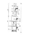
図3は、図1のX−X’断面を示している。図1にて既に説明したものについては同一の符号を付している。図3中、310で示す箇所、つまり搬送コンベア111、移載機101は主搬送路に該当し、320で示す箇所、つまり搬送コンベア131、処理装置Aは、主搬送路から枝状に配置されている。
FIG. 3 shows a cross section of FIG. 1 XX'. The same reference numerals are given to those already described in FIG. In FIG. 3, the location indicated by 310, that is, the
基板投入取出口110には、投入を待つ基板カセット301が設置されている。搬送アーム302は、基板カセット301から被処理基板を取り出し、搬送コンベア111に移送する。図3中、搬送コンベア111は二層式として示されている。これは、主搬送路において被処理基板が同時期に行き来する場合の効率化を狙ったものである。図3に示す通り、上層側コンベア、及び下層側コンベアの一方を往路方向、他方を復路方向とする一方向搬送型でも良いし、各々が自由に往復可能な双方向搬送型であっても良い。この構成によって、複数の被処理基板が主搬送路をすれ違うことが可能となる。また、図3において、搬送コンベア111は上下に二層が重なっているが、これに限定するものではなく、水平方向あるいは斜め方向に二層が並んでいても良い。
A
移載機101は搬送アーム161を有し、主搬送路の搬送コンベア111と搬送コンベア112(図3には図示せず)との間、又は主搬送路の搬送コンベア111と処理装置Aの搬送室191に繋がる搬送コンベア131との間で被処理基板の受け渡しを行う。搬送コンベア131は処理装置Aの搬送室191への被処理基板の受け渡しを行うものであり、この経路においては、同時期に複数の被処理基板が行き来する必要は通常無いため、主搬送路に属する搬送コンベア111と異なり、一層式の双方向搬送型で良い。勿論二層式としても良い。主搬送路と処理装置Aとの距離を十分に近づけることが出来る場合は、搬送コンベア131は単なる被処理基板設置用のステージであっても良い。
The
処理装置Aは、搬送コンベア131から、搬送室191に設けられた搬送アーム152によって被処理基板を取り出し、チャンバ151に投入する。搬送室191には、複数のチャンバが接続されているのが一般的であり、搬送室191と各チャンバの間を被処理基板が往復しながら処理が進行する。処理装置A内での処理が完了すると、被処理基板は搬送コンベア131を戻り、主搬送路に送り出される。
The processing device A takes out the substrate to be processed from the
基板投入口110、搬送コンベア111、移載機101、搬送コンベア131、及び搬送室191は、それぞれポートを介して接続されている。搬送室191には、チャンバ151がポートを介して接続されている。各ポートは、ロードロック扉351〜357を有する。発光素子の製造装置100内で実施される処理のいくつかは、真空又は減圧、あるいは特定の雰囲気を必要とするため、各ロードロック扉は十分な気密性を有している。処理装置内では、各チャンバで異なる雰囲気とすることも可能であり、基板移載の際は、必要最小限の領域だけを開放するようにして、雰囲気置換や減圧を効率化することができる。
The
搬送コンベア111、131はそれぞれ、被処理基板を載せて移動するステージ303を有する。表示装置の製造装置においては、例えばステージ303では、被処理基板が移動中にずれたりステージ303から脱落したりしないように、真空チャック等によって吸着されるが、有機EL素子の蒸着装置等においては、搬送経路が大気曝露されないように真空保持されるため、真空チャックでの吸着が難しい。被処理基板のズレ、脱落防止の一策として、例えばステージ303上に被処理基板を保持するためのピン140を、被処理基板の周端部近傍に当たるように、かつ中央部には当たらないように設けることで、敢えて被処理基板の中央が重力でたわんだ状態で移送する等の手法が考えられる。被処理基板の中央部は、たわみによってピン140の頂点より低い位置となるため、被処理基板の横方向へのズレが防止される。
The
又は、特に図示しないが、ステージ303に被処理基板ホールド用の爪を持たせて、基板の端部、特に成膜に影響の無い箇所を掴んで保持できるようにしても良い。
Alternatively, although not particularly shown, the
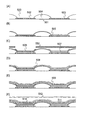
次に、図5を用いて、有機EL素子の製造工程に関して説明する。図5(A)〜(F)は、表示装置500の表示領域の断面図を示している。絶縁表面501上には、画素電極502、503が形成されている。ここで、絶縁表面501の下層には、各画素を制御するためのトランジスタや、発光素子に電流を供給するための配線等が形成されている。画素電極502、503の端部を覆うように、バンク504が形成されている。画素電極502、503の表面のうち、バンク504から露出する領域が、有機EL素子の発光領域となる。画素電極502、503及びバンク504の形成までは、フォトリソグラフィ及びエッチングを用いた工程で行われる。図5(A)まで終了した状態の基板が、前述の被処理基板に該当する。
Next, the manufacturing process of the organic EL element will be described with reference to FIG. 5 (A) to 5 (F) show a cross-sectional view of a display area of the
ここでは、画素電極502、503が、有機EL素子の陽極(ANODE)となる場合の構成について説明する。画素電極502、503が陽極となる場合は、表面に仕事関数の大きい材料を用いることが望まれる。図5(A)において、下側に出射光を取り出す構成をボトムエミッション方式と呼ぶが、この場合、画素電極502、503はITO、IZO、ZnO等の透明導電材料で形成することが好ましい。画素電極が透明であるから光の取り出しが可能であり、かつ仕事関数も大きいため、好適である。反対に、上側に出射光を取り出すトップエミッション方式の場合、画素電極502、503には反射性が求められるため、Ag等が用いられると共に、最表面にITOの層を薄く形成して、表面の仕事関数を大きくする等の構成が挙げられる。
Here, the configuration in which the
図5(B)に示すように、被処理基板上に、まずホール輸送層505を形成する。ホール輸送性材料としては、トリアリールアミン誘導体、又はビススチリルアミン誘導体等が望ましく、代表的な化合物としては、α―NPD、TPD、TPAC、Spiro−TPD、PDA、m−MTDATA等が挙げられる。画素電極502、503の表面の仕事関数によっては、画素電極502、503とホール輸送層505との間に、ホール注入層を設けても良い。また、ホール輸送層505は、画素電極502、503、及びバンク504を覆うように、連続的な膜として設けられているが、画素電極502、503の各々に対して個別に形成されても良い。
As shown in FIG. 5B, the
続いて、図5(C)に示すように、ホール輸送層505上に、発光層506、507を形成する。図5(C)では、画素電極502と重なる領域には発光層506が形成され、画素電極503と重なる領域には発光層507が形成されている。これは、各画素の発光色に合わせて、異なる材料を含む発光層を個別に形成するためである。図5(C)では、発光層506を形成するために、画素電極502と重なる領域に開口を有するマスク550を基板と平行に配置している。これにより、画素電極503と重なる領域には発光層506は形成されない。画素電極503上に発光層507を形成する際には、異なる位置に開口を有するマスク550を用いて、画素電極503と重なる領域のみに発光層507が形成される。図5(C)に示すように、発光色に応じて個別に発光層を形成する場合は、発光色の数だけマスクを使用し、前述の工程を繰り返すことによって行われる。これとは別の方式として、例えば白色発光が得られる材料を用いて、ホール輸送層505等と同様に、画素電極502上から画素電極503上に亘って連続的な発光層を形成する場合もある。この場合、発色は別途設けるカラーフィルタや色変換層が用いられる。
Subsequently, as shown in FIG. 5C, light emitting
発光層506、507の材料としては、アルミニウム錯体、ベリリウム錯体等の金属錯体が代表的である。また、前述の材料をホスト材料とし、微量のドーパントを共蒸着することで発光層506、507を形成しても良い。この場合のドーパント材料としては、イリジウム錯体、ペリレン、ルブレン、クマリン等が代表的である。発光層506、507で所望する発光色に合わせて、前述の材料がそれぞれ選択される。
As the material of the
続いて、図5(D)に示すように、ホール輸送層505、及び発光層506、507上に、電子輸送層508を形成する。電子輸送性材料としては、トリアゾール誘導体、又はオキサジアゾール誘導体等が望ましく、代表的な化合物としては、BND、PBD、TAZ、OXD等が挙げられる。図5(D)においては、電子輸送層508はホール輸送層505、及び発光層506、507を覆うように、連続的な膜として設けられているが、画素電極502、503の各々の上に、個別に形成されても良い。
Subsequently, as shown in FIG. 5D, an
続いて、図5(E)に示すように、電子輸送層508上に、対向電極509を形成する。対向電極509は、有機EL素子の陰極(CATHODE)となるり、代表的には、MgAg、又はAl等が用いられる。これらは金属材料であるため、通常は反射電極として形成される。ボトムエミッション方式の場合、対向電極509は反射電極として構わないが、トップエミッション方式の場合、対向電極509は出射光を透過させる必要があるため、先の金属材料を、10nm〜数10nm程度の薄膜状に形成し、ある程度の透過性を有するように形成される。対向電極509として、ITO、IZO、ZnO等の透明導電材料を用いて形成しても良い。なお、これらの透明導電材料やAlなどは仕事関数が比較的大きいため、電子輸送層508と対向電極509との間に、電子注入層を設けても良い。
Subsequently, as shown in FIG. 5 (E), the
以上で、有機EL素子の形成は完了する。有機EL素子は、大気中の水分により容易に劣化が進行するため、各成膜工程、及びその間の被処理基板の搬送中は大気曝露を避けることが好ましい。従って、製造装置100内は真空、あるいは特定ガス雰囲気が保たれ、その中を被処理基板が移動する構成とすることが好ましい。
This completes the formation of the organic EL element. Since the organic EL element is easily deteriorated by the moisture in the atmosphere, it is preferable to avoid exposure to the atmosphere during each film forming process and during the transportation of the substrate to be processed during the process. Therefore, it is preferable that the inside of the
また、前述の大気中の水分による劣化は、有機EL素子の形成が完了した後であっても進行し得るため、有機EL素子の大気曝露を防ぐことを目的の一つとして、図5(F)に示すように、封止膜を形成しても良い。ここでは、窒化シリコン膜510、有機樹脂膜511、窒化シリコン膜512の3層構造として封止膜を形成している。封止膜の最下層に窒化シリコン膜510を形成することで、高い防湿性を付与することができるため、その後の有機樹脂膜511等の形成においては、大気圧下で実施されても良い。これらの封止膜は、有機EL素子への異物の付着や、鋭利な異物による積層膜の破損等を防止する点でも有用である。
Further, since the above-mentioned deterioration due to moisture in the atmosphere can proceed even after the formation of the organic EL element is completed, FIG. 5 (F) is one of the purposes of preventing the organic EL element from being exposed to the atmosphere. ) May be formed, and a sealing film may be formed. Here, the sealing film is formed as a three-layer structure of the
図5(C)を用いて説明した発光層の形成に際しては、マスク550を発光層の形成面に配置することで所望の箇所にそれぞれの発光層を形成しているが、被処理基板の大判化に伴ってマスクが大型化し、表示装置の高精細化に伴ってマスクの開口領域の割合が増えるため、マスク550自体の剛性が低下する。結果として被処理基板自体やマスク550が重力で撓んで両者の間隔が変わったり、撓みによる位置ズレを起こしたりする。これを回避するため、被処理基板及びマスク550を90度転回し、被処理基板及びマスク550を、垂直に立てた状態に保持して発光層の形成を行っても良い。この場合、図1に示した主搬送路からチャンバ151に被処理基板が搬入されるまでの間で、被処理基板を転回する機構を設ける。
In the formation of the light emitting layer described with reference to FIG. 5C, the
図9に、被処理基板に発光層を形成する工程の概略図を示す。図9(A)は、被処理基板910およびマスク920を水平、つまり、その表面が重力930に平行な方向を向くように保持して発光層の形成を行う例である。具体的には、被処理基板910の下部に設けられた蒸着源901から有機材料を蒸散させ、被処理基板910が蒸着源901に対面する側、つまり下面に発光層が形成される態様を示している。図9(A)において、蒸着源901は、複数の蒸着源が線上に並んだ構成、いわゆるリニアソース型とし、蒸着源901が矢印905の方向に移動する構成を示しているが、これに限定するものではない。図5(C)に示した図においては、概略的に、被処理基板の上面に発光層506が形成されるように示しているが、実際は、蒸着源からの有機材料の蒸散方向の関係上、蒸着源901、被処理基板910、マスク920は、図9(A)のような位置関係となっている。この場合、重力930は被処理基板910およびマスク920の膜厚方向に平行に働くため、両者は撓みを生じやすい。
FIG. 9 shows a schematic view of a process of forming a light emitting layer on a substrate to be processed. FIG. 9A is an example in which the substrate to be processed 910 and the
図9(B)は、被処理基板を垂直、つまり、その表面が重力に垂直な方向を向くように保持して発光層の形成を行う例であり、具体的には、有機材料が横方向に蒸散するように設けられた蒸着源951から、被処理基板910の蒸着源に対面する側に発光層911が形成される態様を示している。図9(B)において、蒸着源951は、複数の蒸着源が線上に並んだ構成、いわゆるリニアソース型とし、蒸着源951が矢印955の方向に移動する構成を示しているが、これに限定するものではない。この場合、重力930は被処理基板910およびマスク920の膜厚方向に垂直に働くため、撓みが生じにくい。
FIG. 9B is an example in which the substrate to be processed is held vertically, that is, the surface thereof is held so as to face the direction perpendicular to gravity to form a light emitting layer. Specifically, the organic material is formed in the lateral direction. The mode in which the light emitting layer 911 is formed on the side of the substrate to be processed 910 facing the vapor deposition source is shown from the
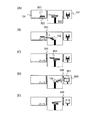
図8は、図3に示した製造装置の断面図における、副搬送路320の異なる態様として、被処理基板を転回する機構を設ける例について示したものである。
FIG. 8 shows an example in which a mechanism for rotating the substrate to be processed is provided as a different aspect of the
図3に示した製造装置の態様においては、被処理基板は、水平な状態で搬送、処理が行われていたのに対し、図8に示す製造装置の態様においては、チャンバ151における処理は、被処理基板を、垂直な状態として行われる。従って、被処理基板を90°転回する機構を搬送アーム152に設けている。
In the aspect of the manufacturing apparatus shown in FIG. 3, the substrate to be processed was conveyed and processed in a horizontal state, whereas in the aspect of the manufacturing apparatus shown in FIG. 8, the processing in the
図8(A)は、副搬送路における搬送コンベア131内のステージ303に、被処理基板801が静置された状態を示している。この状態から、図8(B)に示すように、ロードロック扉355が開き、搬送アーム152がステージ303に静置された被処理基板801を受け取り、処理装置の搬送室191側に被処理基板を引き込む。その後ロードロック扉355が閉じ、搬送室191と副搬送路は空間的に遮断される(図8(C))。
FIG. 8A shows a state in which the substrate to be processed 801 is stationary on the
続いて、図8(D)に示すように、チャンバ151に繋がるロードロック扉356が開き、搬送アーム152は、チャンバ151側に被処理基板801を受け渡す。チャンバ151は、被処理基板を、垂直な状態として処理を行う。搬送アーム152は、アームの途中に回転軸を有する。チャンバ151に被処理基板801を送り込むと同時にアームが回転することで被処理基板801は水平な状態から、垂直な状態に転回する。ステージ802は、被処理基板の端部を挟持する爪を有しており、搬送アーム152が転回した被処理基板801を受け取り、保持する。
Subsequently, as shown in FIG. 8D, the
その後、図8(E)に示すように、ロードロック扉356が閉じ、チャンバ151は空間的に遮断され、処理が行われる。
After that, as shown in FIG. 8E, the
図8においては、搬送室191に設けられた搬送アーム152が回転軸を有しているが、これに限定するものではなく、主搬送路側に設けられた搬送アーム(図8においては図示せず)が回転軸を有していても良い。その場合、副搬送路側に設けられた搬送コンベア131のステージ303も、被処理基板を垂直な状態で保持できる機構を有する。
In FIG. 8, the
搬送室191の搬送アーム152に回転軸を設ける利点としては、搬送室191に接続される複数のチャンバの各々において、被処理基板の保持形式を任意にできる点がある。例えば、搬送室191に接続されたあるチャンバにおいては、被処理基板を水平な状態として処理が行われ、一方で、搬送室191に接続された他のチャンバにおいては、被処理基板を垂直な状態として処理が行われる。
The advantage of providing the rotating shaft on the
図4は、従来の発光素子の製造装置を示しているが、処理装置A〜Eが移載機421〜424及び搬送コンベア411、412を介して、基板投入口401及び基板取出口402の間に直列に接続されている。基板投入口401から投入された被処理基板は、処理装置Aから順にB、C、D、Eと通過する。
FIG. 4 shows a conventional manufacturing device for a light emitting element, in which processing devices A to E are placed between a
このような構成において、処理順序を変更する場合、例えば処理装置Aでの処理の直後に、処理装置Bではなく処理装置Dでの処理を行う場合であっても、介在する処理装置B、Cを経由しなければならない。つまり、基板の動線上に処理装置が配置されているため、処理装置Aでの処理が終了してから処理装置Dの処理を開始するまでの間に、処理装置BおよびCでの基板の処理は出来ない。また、仮に処理装置Aと処理装置Bとの間に、新たに処理装置Fを追加しようとすると、少なくとも処理装置A、搬送コンベア411、基板投入口401の移設が必須となってしまう。従って、図4のような従来の発光素子の製造装置においては、工程の変更及び追加に伴う装置構成の変更は容易ではない。さらに、前述したように、途中の特定の処理装置がボトルネックになる場合、その部分を並列化して全体のスループットを上げるといった手法も、従来の構成では困難である。
In such a configuration, when the processing order is changed, for example, even if the processing is performed by the processing device D instead of the processing device B immediately after the processing by the processing device A, the intervening processing devices B and C are used. Must go through. That is, since the processing device is arranged on the flow line of the substrate, the processing of the substrate by the processing devices B and C is performed between the end of the processing by the processing device A and the start of the processing by the processing device D. I can't. Further, if a new processing device F is to be added between the processing device A and the processing device B, at least the processing device A, the
また、図4に示した発光素子の製造装置は、装置を直列に接続する都合上、基板投入口401と基板取出口402が別になる。一方、図1に示した本発明の発光素子の製造装置は、基板投入取出口110が被処理基板の投入、取り出しを行うため、他の装置やストッカとの被処理基板の受け渡しが簡単であるという利点もある。このように、投入口と取出口を共通とする構成を、インターバック方式と呼んでいる。製造装置100では、基板投入取出口110のみならず、各処理装置A〜Eについても、搬送コンベア131〜135がそれぞれの装置への投入、取り出しを行っているから、インターバック方式が採られている。また、各処理装置をインターバック方式とすることにより、主搬送路に対して枝状に配置することができ、装置間の接続やレイアウトが簡単かつ自由度が高くなる。もちろん、処理装置を配置する環境によっては、基板の投入口と取出口を別とするのが望ましい場合もあるから、適宜構成を選択すれば良い。
Further, in the light emitting element manufacturing apparatus shown in FIG. 4, the
また、図1において、基板投入取出口110、移載機101〜103、及び搬送コンベア111〜113で構成される主搬送路において、移載機103の、搬送コンベア113が接続されている側でない空きポート180の先を、さらに基板投入取出口110に接続して、主搬送路を環状とする構成としても良い。この場合、厳密にはインターバック式ではないが、主搬送路上を進んだ被処理基板が、一周して基板投入取出口110に戻って回収される点ではインターバック式と同等である。
Further, in FIG. 1, in the main transport path composed of the substrate loading / unloading
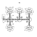
図7に、具体例を示す。発光素子の製造装置700では、基板投入取出口110は搬送コンベア731に接続されており、搬送コンベア731との間で被処理基板の授受を行う。移載機701〜708、及び搬送コンベア731〜738で形成される環状の経路が主搬送路であり、各移載機には、主搬送路を構成する搬送コンベアが接続されるポートを除くポートに、副搬送路を介して処理装置を接続することができる。図7においては、実線で示した処理装置Aの他、さらに点線で示した処理装置B〜H、J〜Lを接続することができる。図7の例では、主搬送路上の移載機701〜708にはそれぞれ、副搬送路を介して1台又は2台の処理装置が接続されているが、配置スペースが許す限りにおいて、3台以上の処理装置が接続されても良い。
FIG. 7 shows a specific example. In the light emitting
さらに、各処理装置に接続するチャンバの数に着目すると、図4に示した従来の構成によると、各処理装置には、前工程からの基板を受け入れる基板投入面と、次工程に基板を流す基板排出面が独立して必要となる。一方、図1に示した本発明の構成においては、各処理装置は主搬送路から枝状に配置されているため、基板投入面と基板排出面は同一で良い。すなわち、1機の処理装置に接続可能なチャンバが1箇所多いという利点もある。 Further, focusing on the number of chambers connected to each processing device, according to the conventional configuration shown in FIG. 4, each processing device has a substrate charging surface for receiving the substrate from the previous process and a substrate flowing to the next process. The board discharge surface is required independently. On the other hand, in the configuration of the present invention shown in FIG. 1, since each processing device is arranged in a branch shape from the main transport path, the substrate loading surface and the substrate discharging surface may be the same. That is, there is also an advantage that there is one more chamber that can be connected to one processing device.
以上のことからも、本発明の発光素子の製造装置の構成の優位性は顕著なものであるといえる。 From the above, it can be said that the superiority of the configuration of the light emitting device manufacturing apparatus of the present invention is remarkable.
付記として、本発明の発光素子の製造装置及び発光素子の製造方法における技術的特徴について以下に列記する。 As a supplement, the technical features of the light emitting device manufacturing apparatus and the light emitting device manufacturing method of the present invention are listed below.
第1受渡室を介して接続された、第1及び第2移載機を有する主搬送路と、前記第1又は第2移載機に接続された第2受渡室、及び前記第2受渡室に接続された搬送室とを有し、前記主搬送路と交差する方向に延在する副搬送路と、前記搬送室に接続された、複数の第1処理室と、を有し、前記主搬送路は、被処理基板を水平な状態で搬送されるように構成され、前記複数の第1処理室の一は、処理中に前記被処理基板を垂直な状態で保持するように構成されたことを特徴とする。 The main transport path having the first and second transfer machines connected via the first delivery room, the second delivery room connected to the first or second transfer machine, and the second delivery room. It has a transport chamber connected to the main transport chamber, an auxiliary transport passage extending in a direction intersecting the main transport passage, and a plurality of first processing chambers connected to the transport chamber. The transport path is configured to transport the substrate to be processed in a horizontal state, and one of the plurality of first processing chambers is configured to hold the substrate to be processed in a vertical state during processing. It is characterized by that.
前記複数の第1処理室の他の一は、処理中に前記被処理基板を水平な状態で保持するように構成されたことを特徴とする。 The other one of the plurality of first processing chambers is characterized in that the substrate to be processed is held in a horizontal state during processing.
第1受渡室を介して接続された、第1及び第2移載機を有する主搬送路と、前記第1移載機に接続された第2受渡室、及び前記第2受渡室に接続された第1搬送室とを有し、前記主搬送路と交差する方向に延在する第1副搬送路と、前記第2移載機に接続された第3受渡室、及び前記第3受渡室に接続された第2搬送室とを有し、前記主搬送路と交差する方向に延在する第2副搬送路と、前記第1搬送室に接続された複数の第1処理室と、前記第2搬送室に接続された複数の第2処理室と、を有し、前記主搬送路は、被処理基板を水平な状態で搬送するように構成され、前記複数の第1処理室の一は、処理中に前記被処理基板を垂直な状態で保持するように構成され、前記複数の第2処理室の一は、処理中に前記被処理基板を水平な状態で保持するように構成されたことを特徴とする。 It is connected to the main transport path having the first and second transfer machines connected via the first delivery room, the second delivery room connected to the first transfer machine, and the second delivery room. A first sub-transport passage that has a first transport chamber and extends in a direction intersecting the main transport passage, a third delivery chamber connected to the second transfer machine, and the third delivery chamber. A second sub-transport passage having a second transport chamber connected to the main transport passage and extending in a direction intersecting the main transport passage, a plurality of first processing chambers connected to the first transport chamber, and the above. It has a plurality of second processing chambers connected to the second transport chamber, and the main transport path is configured to transport the substrate to be processed in a horizontal state, and is one of the plurality of first treatment chambers. Is configured to hold the substrate to be processed in a vertical state during processing, and one of the plurality of second processing chambers is configured to hold the substrate to be processed in a horizontal state during processing. It is characterized by that.
前記第1移載機及び前記第2移載機はそれぞれ、前記第1受渡室が接続される第1ポートと、前記第2受渡室が接続される第2ポートと、前記被処理基板を格納するバッファが接続される第3ポートと、を有し、前記第1搬送室は、前記第2受渡室が接続される第4ポートと、前記複数の第1処理室の一が接続される第5ポートと、を有することを特徴とする。 The first transfer machine and the second transfer machine each store the first port to which the first delivery chamber is connected, the second port to which the second delivery chamber is connected, and the substrate to be processed. The first transport chamber has a third port to which the buffer is connected, and the fourth port to which the second delivery chamber is connected and one of the plurality of first processing chambers are connected. It is characterized by having 5 ports.
前記第1移載機及び前記第2移載機はそれぞれ、前記第1受渡室が接続される第1ポートと、前記第2受渡室が接続される第2ポートと、前記被処理基板を格納するバッファが接続される第3ポートと、を有し、前記第1搬送室及び前記第2搬送室はそれぞれ、前記第2受渡室が接続される第4ポートと、前記複数の第1処理室の一、又は前記複数の第2処理室の一が接続される第5ポートと、を有することを特徴とする。 The first transfer machine and the second transfer machine each store the first port to which the first delivery chamber is connected, the second port to which the second delivery chamber is connected, and the substrate to be processed. The first transport chamber and the second transport chamber have a third port to which the buffer to be connected is connected, and the first transport chamber and the second transport chamber have the fourth port to which the second delivery chamber is connected and the plurality of first processing chambers, respectively. It is characterized by having one or a fifth port to which one of the plurality of second processing chambers is connected.
前記第1移載機、前記第2移載機、及び前記複数の第1処理室の一はそれぞれ、前記被処理基板を運ぶためのアームを有し、前記第1移載機、前記第2移載機、又は前記複数の第1処理室の一が有するアームは、前記被処理基板を水平な状態から垂直な状態、あるいはその逆に転回させるための回転軸を有することを特徴とする。 The first transfer machine, the second transfer machine, and one of the plurality of first processing chambers each have an arm for carrying the substrate to be processed, and the first transfer machine and the second transfer machine. The transfer machine or the arm of one of the plurality of first processing chambers is characterized by having a rotation axis for rotating the substrate to be processed from a horizontal state to a vertical state and vice versa.
前記第1移載機、前記第2移載機、前記複数の第1処理室、及び前記複数の第2処理室の一はそれぞれ、前記被処理基板を運ぶためのアームを有し、前記第1移載機、前記第2移載機、前記第1処理室、又は前記複数の第2処理室の一が有するアームは、前記被処理基板を水平な状態から垂直な状態、あるいはその逆に転回させるための回転軸を有することを特徴とする。 The first transfer machine, the second transfer machine, the plurality of first processing chambers, and one of the plurality of second processing chambers each have an arm for carrying the substrate to be processed, and the first The arm possessed by one transfer machine, the second transfer machine, the first processing chamber, or one of the plurality of second processing chambers causes the substrate to be processed to be in a horizontal state to a vertical state, or vice versa. It is characterized by having a rotation axis for turning.
前記複数の第1処理室はそれぞれ、前記第1搬送室を中心に、放射状に接続されることを特徴とする。 Each of the plurality of first processing chambers is radially connected around the first transport chamber.
前記複数の第1処理室はそれぞれ、前記第1搬送室を中心に、放射状に接続され、前記複数の第2処理室はそれぞれ、前記第2搬送室を中心に、放射状に接続されることを特徴とする。 The plurality of first processing chambers are connected radially around the first transport chamber, and the plurality of second treatment chambers are connected radially around the second transport chamber, respectively. It is a feature.
前記第1乃至第5ポートはそれぞれ、気密性を有することを特徴とする。 Each of the first to fifth ports is characterized by having airtightness.
前記主搬送路上の末端に位置する前記第1又は前記第2移載機の前記第1ポートに、基板投入取出口をさらに有し、処理前の前記被処理基板の投入と、処理済の前記被処理基板の取り出しは、いずれも前記基板投入取出口を介して行われることを特徴とする。 The first port of the first or second transfer machine located at the end on the main transport path further has a substrate loading / unloading port, and the substrate to be processed before processing and the processed substrate have been processed. The substrate to be processed is taken out via the substrate loading / unloading port.
前記主搬送路上の一の末端に位置する前記第1又は前記第2移載機の前記第1ポートに、基板投入口をさらに有し、前記主搬送路上の他の末端に位置する前記第1又は前記第2移載機の前記第1ポートに、基板取出口をさらに有し、処理前の前記被処理基板の投入は、前記基板投入口を介して行われ、処理済の前記被処理基板の取り出しは、前記基板取出口を介して行われることを特徴とする。 The first port of the first or second transfer machine located at one end on the main transport path further has a substrate input port and is located at the other end on the main transport path. Alternatively, the first port of the second transfer machine is further provided with a substrate outlet, and the substrate to be processed before processing is input through the substrate input port, and the processed substrate to be processed has been processed. Is taken out through the substrate take-out port.
前記主搬送路上の前記第1移載機又は前記第2移載機の前記第1ポートに、基板投入取出口をさらに有し、前記主搬送路は、前記第1移載機、前記第1受渡室、前記第2移載機、及び前記基板投入取出口を通る環状経路を有し、処理前の前記被処理基板の投入と、処理済の前記被処理基板の取り出しは、いずれも前記基板投入取出口を介して行われることを特徴とする。 The first transfer machine on the main transport path or the first port of the second transfer machine further has a substrate loading / unloading port, and the main transport path is the first transfer machine, the first. It has an annular path through the delivery chamber, the second transfer machine, and the substrate loading / unloading port, and the loading of the substrate to be processed before processing and the removal of the processed substrate to be processed are all the substrates. It is characterized in that it is performed via an inlet / outlet.
前記主搬送路は、一筆書き形状であることを特徴とする。 The main transport path is characterized in that it has a one-stroke shape.
前記第1受渡室は、少なくとも二つが並行して設けられていることを特徴とする。 The first delivery room is characterized in that at least two are provided in parallel.
第1受渡室を介して接続された、第1及び第2移載機を有する主搬送路と、前記第1又は第2移載機に接続された第2受渡室、及び前記第2受渡室に接続された搬送室とを有し、前記主搬送路と交差する方向に延在する副搬送路と、前記搬送室に接続された、複数の第1処理室と、を有する製造装置を用いた積層膜の製造方法であって、絶縁表面上に、画素電極と、前記画素電極の端部を覆うと共に、前記画素電極の上面の一部を露出するバンクと、を有する被処理基板を用意し、前記被処理基板を、前記製造装置の前記主搬送路上に設けられた前記第1移載機に搬入し、前記被処理基板を、前記第1移載機から、前記第2受渡室を介して前記搬送室に搬入し、前記被処理基板を、前記搬送室から前記複数の第1処理室の一に搬入し、前記被処理基板を水平な状態に保持して、前記画素電極及び前記バンク上に第1有機層を形成し、前記被処理基板を、前記複数の第1処理室の一から前記搬送室に戻し、前記被処理基板を、前記搬送室から前記複数の第1処理室の他の一に搬入し、前記被処理基板を垂直な状態に保持して、前記第1有機層上の、前記画素電極に重畳する領域に第2有機層を形成し、前記被処理基板を、前記複数の第1処理室の他の一から前記搬送室に戻し、前記被処理基板を、前記搬送室から、前記第2受渡室を介して前記第1移載機に戻す工程を含み、前記被処理基板が、前記搬送室から前記複数の第1処理室の他の一に搬入されるまでの間に、前記水平な状態から前記垂直な状態に転回される工程を含む。 The main transport path having the first and second transfer machines connected via the first delivery room, the second delivery room connected to the first or second transfer machine, and the second delivery room. A manufacturing apparatus having a transport chamber connected to the main transport passage, an auxiliary transport passage extending in a direction intersecting the main transport passage, and a plurality of first processing chambers connected to the transport chamber. A substrate to be processed is prepared, which is a method for manufacturing a laminated film, which has a pixel electrode and a bank that covers an end portion of the pixel electrode and exposes a part of the upper surface of the pixel electrode on an insulating surface. Then, the substrate to be processed is carried into the first transfer machine provided on the main transport path of the manufacturing apparatus, and the substrate to be processed is transferred from the first transfer machine to the second delivery chamber. The substrate to be processed is carried into one of the plurality of first processing chambers from the transport chamber, and the substrate to be processed is held in a horizontal state, and the pixel electrode and the said substrate are carried into the transport chamber. A first organic layer is formed on the bank, the substrate to be processed is returned from one of the plurality of first processing chambers to the transport chamber, and the substrate to be processed is transferred from the transport chamber to the plurality of first treatment chambers. The substrate to be processed is carried into another one, the substrate to be processed is held in a vertical state, a second organic layer is formed in a region on the first organic layer superimposing on the pixel electrodes, and the substrate to be processed is formed. , The step of returning the substrate to be processed from the other one of the plurality of first processing chambers to the transport chamber, and returning the substrate to be processed from the transport chamber to the first transfer machine via the second delivery chamber. The step of turning the substrate to be processed from the horizontal state to the vertical state is included in the process of being carried from the transport chamber to the other one of the plurality of first processing chambers.
第1受渡室を介して接続された、第1及び第2移載機を有する主搬送路と、前記第1移載機に接続された第2受渡室、及び前記第2受渡室に接続された第1搬送室とを有し、前記主搬送路と交差する方向に延在する第1副搬送路と、前記第2移載機に接続された第3受渡室、及び前記第3受渡室に接続された第2搬送室とを有し、前記主搬送路と交差する方向に延在する第2副搬送路と、前記第1搬送室に接続された複数の第1処理室と、前記第2搬送室に接続された複数の第2処理室と、を有する製造装置を用いた積層膜の製造方法であって、絶縁表面上に、画素電極と、前記画素電極の端部を覆うと共に、前記画素電極の上面の一部を露出するバンクと、を有する被処理基板を用意し、前記被処理基板を、前記製造装置の前記主搬送路上に設けられた前記第1移載機に搬入し、前記被処理基板を、前記第1移載機から、前記第2受渡室を介して前記第1搬送室に搬入し、前記被処理基板を、前記第1搬送室から前記複数の第1処理室の一に搬入し、前記被処理基板を水平な状態に保持して、前記画素電極及び前記バンク上に第1有機層を形成し、前記被処理基板を、前記複数の第1処理室の一から前記第1搬送室に戻し、前記被処理基板を、前記第1搬送室から、前記第2受渡室を介して前記第1移載機に戻し、前記被処理基板を、前記第1移載機から、前記第1受渡室を介して前記第2移載機に搬入し、前記被処理基板を、前記第2移載機から、前記第3受渡室を介して前記第2搬送室に搬入し、前記被処理基板を、前記第2搬送室から前記複数の第2処理室の一に搬入し、前記被処理基板を垂直な状態に保持して、前記第1有機層上の、前記画素電極に重畳する領域に第2有機層を形成し、前記被処理基板を、前記第2処理室の一から前記第2搬送室に戻し、前記被処理基板を、前記第2搬送室から、前記第3受渡室を介して前記第2移載機に戻す工程を含み、前記被処理基板が、前記第2移載機から前記第2搬送室に搬入されるまでの間、又は前記第2搬送室から前記複数の第2処理室の一に搬入されるまでの間に、前記水平な状態から前記垂直な状態に転回される工程を含む。 It is connected to the main transport path having the first and second transfer machines connected via the first delivery room, the second delivery room connected to the first transfer machine, and the second delivery room. A first sub-transport passage that has a first transport chamber and extends in a direction intersecting the main transport passage, a third delivery chamber connected to the second transfer machine, and the third delivery chamber. A second transport passage having a second transport chamber connected to the main transport passage and extending in a direction intersecting the main transport passage, a plurality of first processing chambers connected to the first transport chamber, and the above. A method for manufacturing a laminated film using a manufacturing apparatus having a plurality of second processing chambers connected to a second transport chamber, in which a pixel electrode and an end portion of the pixel electrode are covered on an insulating surface. A substrate to be processed having a bank for exposing a part of the upper surface of the pixel electrode is prepared, and the substrate to be processed is carried into the first transfer machine provided on the main transport path of the manufacturing apparatus. Then, the substrate to be processed is carried from the first transfer machine into the first transport chamber via the second delivery chamber, and the substrate to be processed is carried from the first transport chamber to the plurality of first transport chambers. It is carried into one of the processing chambers, the substrate to be processed is held in a horizontal state, a first organic layer is formed on the pixel electrodes and the bank, and the substrate to be processed is placed in the plurality of first processing chambers. Returning from 1 to the 1st transport chamber, the substrate to be processed is returned from the 1st transport chamber to the 1st transfer machine via the 2nd delivery chamber, and the substrate to be processed is returned to the 1st transfer chamber. The transfer machine is carried into the second transfer machine via the first transfer chamber, and the substrate to be processed is transferred from the second transfer machine through the third transfer chamber to the second transfer chamber. The substrate to be processed is carried from the second transport chamber into one of the plurality of second processing chambers, and the substrate to be processed is held in a vertical state on the first organic layer. A second organic layer is formed in the region superposed on the pixel electrodes, the substrate to be processed is returned from one of the second processing chambers to the second transport chamber, and the substrate to be processed is transferred from the second transport chamber. , Including the step of returning to the second transfer machine via the third delivery chamber, until the substrate to be processed is carried from the second transfer machine into the second transfer chamber, or the first. (2) The step of turning from the horizontal state to the vertical state is included in the process of being carried from the transport chamber to one of the plurality of second processing chambers.
前記第1有機層は、発光素子のホール輸送層又は電子輸送層を含むことを特徴とする。 The first organic layer is characterized by including a hole transport layer or an electron transport layer of the light emitting device.
前記第2有機層は、発光素子の発光層を含むことを特徴とする。 The second organic layer is characterized by including a light emitting layer of a light emitting element.
100,700:発光素子の製造装置、101〜103,421〜424,701〜708:移載機、111〜113,131〜135,411,412,610,620,731〜738:搬送コンベア、191〜195:搬送室、110:基板投入取出口、140:ピン、151:チャンバ、152,161,302:搬送アーム、153,351〜357:ロードロック扉、154,163〜165:空きポート、162:バッファ、301:基板カセット、303:ステージ、401:基板投入口、402:基板取出口、500:表示装置、501:絶縁表面、502,503:画素電極、504:バンク、505:ホール輸送層、506,507:発光層、508:電子輸送層、509:対向電極、510,512:窒化シリコン膜、511:有機樹脂膜、550:マスク、601〜604:処理室、910:被処理基板、920:マスク、901,951:蒸着源 100, 700: Light emitting element manufacturing apparatus, 101-103, 421-424, 701-708: Transfer machine, 111-113, 131-135, 411, 421, 610, 620, 731-738: Conveyance conveyor, 191 ~ 195: Conveyance chamber, 110: Board loading / unloading, 140: Pin, 151: Chamber, 152,161,302: Conveying arm, 153,351-357: Load lock door, 154,163 ~ 165: Empty port, 162 : Buffer, 301: Substrate cassette, 303: Stage, 401: Substrate inlet, 402: Substrate outlet, 500: Display device, 501: Insulated surface, 502,503: Pixel electrode, 504: Bank, 505: Hall transport layer , 506, 507: Light emitting layer, 508: Electron transport layer, 509: Counter electrode, 510, 512: Silicon nitride film, 511: Organic resin film, 550: Mask, 601-604: Processing chamber, 910: Substrate to be processed, 920: Mask, 901, 951: Deposition source
Claims (17)
前記第1又は第2移載機に接続された第2受渡室、及び前記第2受渡室に接続された搬送室とを有し、前記主搬送路と交差する方向に延在する副搬送路と、
前記搬送室に接続された、複数の第1処理室と、を有し、
前記主搬送路は、被処理基板を水平な状態で搬送されるように構成され、
前記複数の第1処理室の一は、処理中に前記被処理基板を垂直な状態で保持するように構成され、
前記搬送室は、前記被処理基板を搬送するためのアームを有し、
前記アームは、前記被処理基板を水平な状態と垂直な状態との間で転回させるための回転軸を有することを特徴とする、積層膜の製造装置。 A main transport path having first and second transfer machines connected via a first delivery room, and
A secondary transport path having a second delivery chamber connected to the first or second transfer machine and a transport chamber connected to the second transfer chamber, and extending in a direction intersecting the main transport path. When,
It has a plurality of first processing chambers connected to the transport chamber.
The main transport path is configured to transport the substrate to be processed in a horizontal state.
One of the plurality of first processing chambers is configured to hold the substrate to be processed in a vertical state during processing .
The transport chamber has an arm for transporting the substrate to be processed.
The arm is a laminated film manufacturing apparatus, characterized in that the arm has a rotation axis for rotating the substrate to be processed between a horizontal state and a vertical state .
前記第1移載機に接続された第2受渡室、及び前記第2受渡室に接続された第1搬送室とを有し、前記主搬送路と交差する方向に延在する第1副搬送路と、
前記第2移載機に接続された第3受渡室、及び前記第3受渡室に接続された第2搬送室とを有し、前記主搬送路と交差する方向に延在する第2副搬送路と、
前記第1搬送室に接続された複数の第1処理室と、
前記第2搬送室に接続された複数の第2処理室と、を有し、
前記主搬送路は、被処理基板を水平な状態で搬送するように構成され、
前記複数の第1処理室の一は、処理中に前記被処理基板を垂直な状態で保持するように構成され、
前記複数の第2処理室の一は、処理中に前記被処理基板を水平な状態で保持するように構成され、
前記第1搬送室、及び前記第2搬送室はそれぞれ、前記被処理基板を搬送するためのアームを有し、
前記アームは、前記被処理基板を水平な状態と垂直な状態との間で転回させるための回転軸を有することを特徴とする、積層膜の製造装置。 A main transport path having first and second transfer machines connected via a first delivery room, and
A first sub-transport that has a second delivery chamber connected to the first transfer machine and a first transport chamber connected to the second delivery chamber and extends in a direction intersecting the main transport path. Road and
A second sub-transport that has a third delivery chamber connected to the second transfer machine and a second transport chamber connected to the third delivery chamber and extends in a direction intersecting the main transport path. Road and
A plurality of first processing chambers connected to the first transport chamber,
It has a plurality of second processing chambers connected to the second transport chamber, and has.
The main transport path is configured to transport the substrate to be processed in a horizontal state.
One of the plurality of first processing chambers is configured to hold the substrate to be processed in a vertical state during processing.
One of the plurality of second processing chambers is configured to hold the substrate to be processed in a horizontal state during processing .
The first transport chamber and the second transport chamber each have an arm for transporting the substrate to be processed.
The arm is a laminated film manufacturing apparatus, characterized in that the arm has a rotation axis for rotating the substrate to be processed between a horizontal state and a vertical state .
前記第1受渡室が接続される第1ポートと、前記第2受渡室が接続される第2ポートと、前記被処理基板を格納するバッファが接続される第3ポートと、を有し、
前記第1搬送室は、前記第2受渡室が接続される第4ポートと、前記複数の第1処理室の一が接続される第5ポートと、を有することを特徴とする、請求項3に記載の製造装置。 The first transfer machine and the second transfer machine are each
It has a first port to which the first delivery chamber is connected, a second port to which the second delivery chamber is connected, and a third port to which a buffer for storing the substrate to be processed is connected.
The first transfer chamber, and having a fourth port and the second delivery chamber is connected, the the fifth port in which one of the plurality of first process chamber is connected to, claim 3 The manufacturing apparatus described in.
前記第1受渡室が接続される第1ポートと、前記第2受渡室が接続される第2ポートと、前記被処理基板を格納するバッファが接続される第3ポートと、を有し、
前記第1搬送室及び前記第2搬送室はそれぞれ、前記第2受渡室が接続される第4ポートと、前記複数の第1処理室の一、又は前記複数の第2処理室の一が接続される第5ポートと、を有することを特徴とする、請求項3に記載の製造装置。 The first transfer machine and the second transfer machine are each
It has a first port to which the first delivery chamber is connected, a second port to which the second delivery chamber is connected, and a third port to which a buffer for storing the substrate to be processed is connected.
The first transport chamber and the second transport chamber are each connected to a fourth port to which the second delivery chamber is connected and one of the plurality of first processing chambers or one of the plurality of second processing chambers. The manufacturing apparatus according to claim 3, further comprising a fifth port.
前記複数の第2処理室は、前記第2搬送室を中心として、放射状に前記第2搬送室に接続されることを特徴とする、請求項3に記載の製造装置。 The plurality of first processing chambers are radially connected to the first transport chamber with the first transport chamber as a center.
The manufacturing apparatus according to claim 3, wherein the plurality of second processing chambers are radially connected to the second transport chamber with the second transport chamber as a center.
前記基板投入取出口は、処理前の前記被処理基板、および処理後の前記被処理基板が前記基板投入取出口を介して投入/取出できるように構成される、請求項1に記載の製造装置。 Further having a substrate loading / unloading port connected to the first transfer machine or the second transfer machine located at the end on the main transport path via another first delivery chamber .
The manufacturing apparatus according to claim 1, wherein the substrate loading / unloading port is configured so that the substrate to be processed before processing and the substrate to be processed after processing can be loaded / unloaded via the substrate loading / unloading port. ..
前記主搬送路上の他の末端に位置する前記第2移載機又は第1移載機に、基板取出口をさらに有し、
前記基板投入口は、処理前の前記被処理基板が前記基板投入口を介して投入できるように構成され、
前記基板取出口は、処理後の前記被処理基板が前記基板取出口を介して取出できるように構成される、請求項1に記載の製造装置。 The first transfer machine or the second transfer machine located at one end on the main transport path further has a substrate input port.
The second transfer machine or the first transfer machine located at the other end on the main transport path further has a substrate outlet.
The substrate input port is configured so that the substrate to be processed before processing can be input through the substrate input port.
The manufacturing apparatus according to claim 1, wherein the substrate outlet is configured so that the processed substrate to be processed can be taken out through the substrate outlet.
前記主搬送路は、前記第1移載機、前記第1受渡室、前記第2移載機、及び前記基板投入取出口を通る環状経路を有し、
前記基板投入取出口は、処理前の前記被処理基板、および処理後の前記被処理基板が前記基板投入取出口を介して投入/取出できるように構成される、請求項4に記載の製造装置。 Further having a substrate loading / unloading port connected to the first port of the first transfer machine or the second transfer machine on the main transport path via another first delivery chamber .
The main transport path has an annular path passing through the first transfer machine, the first delivery chamber, the second transfer machine, and the substrate loading / unloading port.
The manufacturing apparatus according to claim 4 , wherein the substrate loading / unloading port is configured so that the substrate to be processed before processing and the substrate to be processed after processing can be loaded / unloaded via the substrate loading / unloading port. ..
前記第1又は第2移載機に接続された第2受渡室、及び前記第2受渡室に接続された搬送室とを有し、前記主搬送路と交差する方向に延在する副搬送路と、
前記搬送室に接続された、複数の第1処理室と、を有する製造装置を用いた積層膜の製造方法であって、
絶縁表面を有し、前記絶縁表面上の画素電極と、前記画素電極の端部を覆うと共に、前記画素電極の上面の一部を露出するバンクと、を有する被処理基板を用意し、
前記被処理基板を、前記製造装置の前記主搬送路上に設けられた前記第1移載機に搬入し、
前記被処理基板を、前記第1移載機から、前記第2受渡室を介して前記搬送室に搬入し、
前記被処理基板を、前記搬送室から前記複数の第1処理室の一に搬入し、
前記被処理基板を水平な状態に保持して、前記画素電極及び前記バンク上に第1有機層を形成し、
前記被処理基板を、前記複数の第1処理室の一から前記搬送室に戻し、
前記搬送室内で、前記被処理基板を水平な状態から垂直な状態に転回し、
前記被処理基板を、前記搬送室から前記複数の第1処理室の他の一に搬入し、
前記被処理基板を垂直な状態に保持して、前記第1有機層上の、前記画素電極に重畳する領域に第2有機層を形成し、
前記被処理基板を、前記複数の第1処理室の他の一から前記搬送室に戻し、
前記搬送室内で、前記被処理基板を垂直な状態から水平な状態に転回し、
前記被処理基板を、前記搬送室から、前記第2受渡室を介して前記第1移載機に戻す工程を含む、積層膜の製造方法。 A main transport path having first and second transfer machines connected via a first delivery room, and
A secondary transport path having a second delivery chamber connected to the first or second transfer machine and a transport chamber connected to the second transfer chamber, and extending in a direction intersecting the main transport path. When,
A method for manufacturing a laminated film using a manufacturing apparatus having a plurality of first processing chambers connected to the transport chamber.
A substrate to be processed having an insulating surface, a pixel electrode on the insulating surface, and a bank that covers the end portion of the pixel electrode and exposes a part of the upper surface of the pixel electrode is prepared.
The substrate to be processed is carried into the first transfer machine provided on the main transport path of the manufacturing apparatus.
The substrate to be processed is carried from the first transfer machine into the transport chamber via the second delivery chamber.
The substrate to be processed is carried from the transport chamber into one of the plurality of first processing chambers.
The substrate to be processed is held in a horizontal state to form a first organic layer on the pixel electrode and the bank.
The substrate to be processed is returned from one of the plurality of first processing chambers to the transport chamber.
In the transport chamber, the substrate to be processed is rotated from a horizontal state to a vertical state.
The substrate to be processed is carried from the transport chamber to another one of the plurality of first processing chambers.
The substrate to be processed is held in a vertical state, and a second organic layer is formed on the first organic layer in a region superposed on the pixel electrodes.
The substrate to be processed is returned to the transport chamber from the other one of the plurality of first processing chambers.
In the transport chamber, the substrate to be processed is rotated from a vertical state to a horizontal state.
A method for producing a laminated film, which comprises a step of returning the substrate to be processed from the transport chamber to the first transfer machine via the second delivery chamber.
前記第1移載機に接続された第2受渡室、及び前記第2受渡室に接続された第1搬送室とを有し、前記主搬送路と交差する方向に延在する第1副搬送路と、
前記第2移載機に接続された第3受渡室、及び前記第3受渡室に接続された第2搬送室とを有し、前記主搬送路と交差する方向に延在する第2副搬送路と、
前記第1搬送室に接続された複数の第1処理室と、
前記第2搬送室に接続された複数の第2処理室と、を有する製造装置を用いた積層膜の製造方法であって、
絶縁表面上に、画素電極と、前記画素電極の端部を覆うと共に、前記画素電極の上面の一部を露出するバンクと、を有する被処理基板を用意し、
前記被処理基板を、前記製造装置の前記主搬送路上に設けられた前記第1移載機に搬入し、
前記被処理基板を、前記第1移載機から、前記第2受渡室を介して前記第1搬送室に搬入し、
前記被処理基板を、前記第1搬送室から前記複数の第1処理室の一に搬入し、
前記被処理基板を水平な状態に保持して、前記画素電極及び前記バンク上に第1有機層を形成し、
前記被処理基板を、前記複数の第1処理室の一から前記第1搬送室に戻し、
前記被処理基板を、前記第1搬送室から、前記第2受渡室を介して前記第1移載機に戻し、
前記被処理基板を、前記第1移載機から、前記第1受渡室を介して前記第2移載機に搬入し、
前記被処理基板を、前記第2移載機から、前記第3受渡室を介して前記第2搬送室に搬入し、
前記第2搬送室内で、前記被処理基板を水平な状態から垂直な状態に転回し、
前記被処理基板を、前記第2搬送室から前記複数の第2処理室の一に搬入し、
前記被処理基板を垂直な状態に保持して、前記第1有機層上の、前記画素電極に重畳する領域に第2有機層を形成し、
前記被処理基板を、前記第2処理室の一から前記第2搬送室に戻し、
前記第2搬送室内で、前記被処理基板を垂直な状態から水平な状態に転回し、
前記被処理基板を、前記第2搬送室から、前記第3受渡室を介して前記第2移載機に戻す工程を含む、積層膜の製造方法。 A main transport path having first and second transfer machines connected via a first delivery room, and
A first sub-transport that has a second delivery chamber connected to the first transfer machine and a first transport chamber connected to the second delivery chamber and extends in a direction intersecting the main transport path. Road and
A second sub-transport that has a third delivery chamber connected to the second transfer machine and a second transport chamber connected to the third delivery chamber and extends in a direction intersecting the main transport path. Road and
A plurality of first processing chambers connected to the first transport chamber,
A method for manufacturing a laminated film using a manufacturing apparatus having a plurality of second processing chambers connected to the second transport chamber.
A substrate to be processed having a pixel electrode and a bank that covers the end portion of the pixel electrode and exposes a part of the upper surface of the pixel electrode is prepared on the insulating surface.
The substrate to be processed is carried into the first transfer machine provided on the main transport path of the manufacturing apparatus.
The substrate to be processed is carried from the first transfer machine into the first transport chamber via the second delivery chamber.
The substrate to be processed is carried from the first transport chamber into one of the plurality of first processing chambers.
The substrate to be processed is held in a horizontal state to form a first organic layer on the pixel electrode and the bank.
The substrate to be processed is returned from one of the plurality of first processing chambers to the first transport chamber.
The substrate to be processed is returned from the first transport chamber to the first transfer machine via the second delivery chamber.
The substrate to be processed is carried from the first transfer machine to the second transfer machine via the first delivery chamber.
The substrate to be processed is carried from the second transfer machine into the second transport chamber via the third delivery chamber.
In the second transport chamber, the substrate to be processed is rotated from a horizontal state to a vertical state.
The substrate to be processed is carried from the second transport chamber into one of the plurality of second processing chambers.
The substrate to be processed is held in a vertical state, and a second organic layer is formed on the first organic layer in a region superposed on the pixel electrodes.
The substrate to be processed is returned from one of the second processing chambers to the second transport chamber.
In the second transport chamber, the substrate to be processed is rotated from a vertical state to a horizontal state.
A method for producing a laminated film, which comprises a step of returning the substrate to be processed from the second transport chamber to the second transfer machine via the third delivery chamber.
The production method according to claim 14 or 15 , wherein the second organic layer includes a light emitting layer of a light emitting element.
Priority Applications (9)
| Application Number | Priority Date | Filing Date | Title |
|---|---|---|---|
| JP2016153361A JP6830772B2 (en) | 2016-08-04 | 2016-08-04 | Laminated film manufacturing equipment and laminated film manufacturing method |
| TW106114597A TWI671918B (en) | 2016-08-04 | 2017-05-03 | Light-emitting element manufacturing apparatus and method of manufacturing same |
| KR1020170082506A KR101953268B1 (en) | 2016-08-04 | 2017-06-29 | Manufacturing device of light emitting element and manufacturing method thereof |
| US15/644,923 US10164218B2 (en) | 2016-08-04 | 2017-07-10 | Manufacturing device and manufacturing method of light-emitting element |
| CN202010289273.8A CN111463365B (en) | 2016-08-04 | 2017-08-04 | Apparatus and method for manufacturing light-emitting element |
| CN201710662741.XA CN107689429A (en) | 2016-08-04 | 2017-08-04 | Light-emitting element manufacturing device and manufacturing method |
| US16/162,528 US10367174B2 (en) | 2016-08-04 | 2018-10-17 | Manufacturing method of a light emitting device |
| KR1020190021103A KR102039090B1 (en) | 2016-08-04 | 2019-02-22 | Manufacturing method of light emitting element |
| US16/447,478 US20190305259A1 (en) | 2016-08-04 | 2019-06-20 | Manufacturing device for light emitting element |
Applications Claiming Priority (1)
| Application Number | Priority Date | Filing Date | Title |
|---|---|---|---|
| JP2016153361A JP6830772B2 (en) | 2016-08-04 | 2016-08-04 | Laminated film manufacturing equipment and laminated film manufacturing method |
Publications (3)
| Publication Number | Publication Date |
|---|---|
| JP2018022619A JP2018022619A (en) | 2018-02-08 |
| JP2018022619A5 JP2018022619A5 (en) | 2019-09-05 |
| JP6830772B2 true JP6830772B2 (en) | 2021-02-17 |
Family
ID=61070200
Family Applications (1)
| Application Number | Title | Priority Date | Filing Date |
|---|---|---|---|
| JP2016153361A Active JP6830772B2 (en) | 2016-08-04 | 2016-08-04 | Laminated film manufacturing equipment and laminated film manufacturing method |
Country Status (5)
| Country | Link |
|---|---|
| US (3) | US10164218B2 (en) |
| JP (1) | JP6830772B2 (en) |
| KR (2) | KR101953268B1 (en) |
| CN (2) | CN111463365B (en) |
| TW (1) | TWI671918B (en) |
Families Citing this family (8)
| Publication number | Priority date | Publication date | Assignee | Title |
|---|---|---|---|---|
| JP6830772B2 (en) * | 2016-08-04 | 2021-02-17 | 株式会社ジャパンディスプレイ | Laminated film manufacturing equipment and laminated film manufacturing method |
| KR102260368B1 (en) * | 2018-03-09 | 2021-06-02 | 어플라이드 머티어리얼스, 인코포레이티드 | Vacuum processing system and method of operation of vacuum processing system |
| KR20200002242A (en) * | 2018-06-29 | 2020-01-08 | 캐논 톡키 가부시키가이샤 | Film forming apparatus, manufacturing apparatus of organic device, and manufacturing method of organic device |
| JP7240980B2 (en) * | 2019-07-29 | 2023-03-16 | 東京エレクトロン株式会社 | SUBSTRATE PROCESSING APPARATUS AND SUBSTRATE CONVEYING METHOD |
| TWI867219B (en) * | 2020-05-12 | 2024-12-21 | 荷蘭商Asm Ip私人控股有限公司 | Semiconductor processing system |
| JP7756109B2 (en) * | 2020-12-25 | 2025-10-17 | 株式会社半導体エネルギー研究所 | Display device manufacturing equipment |
| JPWO2023285913A1 (en) * | 2021-07-16 | 2023-01-19 | ||
| JP7747470B2 (en) * | 2021-09-06 | 2025-10-01 | キヤノントッキ株式会社 | Film forming apparatus, substrate transfer apparatus, substrate transfer method, and electronic device manufacturing method |
Family Cites Families (31)
| Publication number | Priority date | Publication date | Assignee | Title |
|---|---|---|---|---|
| JPH07211762A (en) * | 1994-01-13 | 1995-08-11 | Hitachi Ltd | Wafer transfer processing equipment |
| JPH07230942A (en) * | 1994-02-18 | 1995-08-29 | Hitachi Ltd | Multi-chamber system and control method thereof |
| JPH08181184A (en) * | 1994-12-22 | 1996-07-12 | Hitachi Ltd | Method of configuring semiconductor manufacturing line |
| TW442891B (en) * | 1998-11-17 | 2001-06-23 | Tokyo Electron Ltd | Vacuum processing system |
| JP3806802B2 (en) * | 2001-04-25 | 2006-08-09 | 株式会社アイテック | Robot hand drive device |
| US6852194B2 (en) * | 2001-05-21 | 2005-02-08 | Tokyo Electron Limited | Processing apparatus, transferring apparatus and transferring method |
| JP4078813B2 (en) * | 2001-06-12 | 2008-04-23 | ソニー株式会社 | Film forming apparatus and film forming method |
| JP4096353B2 (en) * | 2002-05-09 | 2008-06-04 | ソニー株式会社 | Organic electroluminescence display device manufacturing apparatus and manufacturing method |
| US7988398B2 (en) * | 2002-07-22 | 2011-08-02 | Brooks Automation, Inc. | Linear substrate transport apparatus |
| CN2587883Y (en) * | 2002-12-19 | 2003-11-26 | 铼宝科技股份有限公司 | Deposition equipment for organic light-emitting components |
| JP2004288463A (en) * | 2003-03-20 | 2004-10-14 | Semiconductor Energy Lab Co Ltd | manufacturing device |
| US20050113976A1 (en) * | 2003-11-10 | 2005-05-26 | Blueshift Technologies, Inc. | Software controller for handling system |
| US8313277B2 (en) * | 2003-11-10 | 2012-11-20 | Brooks Automation, Inc. | Semiconductor manufacturing process modules |
| JP5128918B2 (en) * | 2007-11-30 | 2013-01-23 | 株式会社Sokudo | Substrate processing equipment |
| EP2098609B1 (en) * | 2008-03-05 | 2012-08-15 | Applied Materials, Inc. | Coating apparatus with rotation module |
| US9353436B2 (en) * | 2008-03-05 | 2016-05-31 | Applied Materials, Inc. | Coating apparatus with rotation module |
| JP4934619B2 (en) * | 2008-03-17 | 2012-05-16 | 株式会社アルバック | Organic EL manufacturing apparatus and organic EL manufacturing method |
| CN101667630A (en) * | 2008-09-04 | 2010-03-10 | 株式会社日立高新技术 | Organic EL device manufacturing apparatus and manufacturing method thereof, and film forming apparatus and film forming method |
| TWI424784B (en) * | 2008-09-04 | 2014-01-21 | 日立全球先端科技股份有限公司 | Organic electroluminescent device manufacturing apparatus, manufacturing method thereof, film forming apparatus and film forming method |
| WO2011059749A2 (en) * | 2009-10-28 | 2011-05-19 | Applied Materials, Inc. | Vertically integrated processing chamber |
| EP2489759B1 (en) * | 2011-02-21 | 2014-12-10 | Applied Materials, Inc. | System for utilization improvement of process chambers and method of operating thereof |
| WO2013077322A1 (en) * | 2011-11-23 | 2013-05-30 | 日本電産サンキョー株式会社 | Work transfer system |
| WO2013090181A1 (en) * | 2011-12-12 | 2013-06-20 | Applied Materials, Inc | Fully-independent robot systems, apparatus, and methods adapted to transport multiple substrates in electronic device manufacturing |
| KR20130074307A (en) * | 2011-12-26 | 2013-07-04 | 엘아이지에이디피 주식회사 | Evaporation device for manufacturing of oled having apparatus for chucking and dechucking |
| JP6079200B2 (en) * | 2012-05-16 | 2017-02-15 | 東京エレクトロン株式会社 | Cooling mechanism and processing system |
| KR20140050994A (en) * | 2012-10-22 | 2014-04-30 | 삼성디스플레이 주식회사 | Organic light emitting display apparatus and method for manufacturing the same |
| KR101990555B1 (en) * | 2012-12-24 | 2019-06-19 | 삼성디스플레이 주식회사 | Thin film encapsulation manufacturing device and manufacturing method of thin film encapsulation |
| JP2015007263A (en) * | 2013-06-24 | 2015-01-15 | 株式会社日立ハイテクノロジーズ | Organic device manufacturing apparatus and organic device manufacturing method |
| KR20160087953A (en) * | 2015-01-14 | 2016-07-25 | 에스엔유 프리시젼 주식회사 | Cluster type evaporation device for manufacturing of OLED |
| JP6937549B2 (en) * | 2016-06-10 | 2021-09-22 | 株式会社ジャパンディスプレイ | Light emitting element manufacturing equipment |
| JP6830772B2 (en) * | 2016-08-04 | 2021-02-17 | 株式会社ジャパンディスプレイ | Laminated film manufacturing equipment and laminated film manufacturing method |
-
2016
- 2016-08-04 JP JP2016153361A patent/JP6830772B2/en active Active
-
2017
- 2017-05-03 TW TW106114597A patent/TWI671918B/en active
- 2017-06-29 KR KR1020170082506A patent/KR101953268B1/en active Active
- 2017-07-10 US US15/644,923 patent/US10164218B2/en active Active
- 2017-08-04 CN CN202010289273.8A patent/CN111463365B/en active Active
- 2017-08-04 CN CN201710662741.XA patent/CN107689429A/en active Pending
-
2018
- 2018-10-17 US US16/162,528 patent/US10367174B2/en active Active
-
2019
- 2019-02-22 KR KR1020190021103A patent/KR102039090B1/en active Active
- 2019-06-20 US US16/447,478 patent/US20190305259A1/en not_active Abandoned
Also Published As
| Publication number | Publication date |
|---|---|
| TW201806178A (en) | 2018-02-16 |
| TWI671918B (en) | 2019-09-11 |
| CN111463365B (en) | 2023-05-26 |
| KR20190022594A (en) | 2019-03-06 |
| US10164218B2 (en) | 2018-12-25 |
| US20190051867A1 (en) | 2019-02-14 |
| KR20180016253A (en) | 2018-02-14 |
| US10367174B2 (en) | 2019-07-30 |
| KR101953268B1 (en) | 2019-02-28 |
| US20190305259A1 (en) | 2019-10-03 |
| CN111463365A (en) | 2020-07-28 |
| JP2018022619A (en) | 2018-02-08 |
| CN107689429A (en) | 2018-02-13 |
| US20180040856A1 (en) | 2018-02-08 |
| KR102039090B1 (en) | 2019-11-01 |
Similar Documents
| Publication | Publication Date | Title |
|---|---|---|
| JP6830772B2 (en) | Laminated film manufacturing equipment and laminated film manufacturing method | |
| JP6937549B2 (en) | Light emitting element manufacturing equipment | |
| JP7148587B2 (en) | Film forming apparatus and method for manufacturing electronic device | |
| US20160240403A1 (en) | Apparatus and method of manufacturing display device | |
| CN110387526A (en) | Treatment body storage device, treatment body storage method, and vapor deposition method | |
| KR101409808B1 (en) | Substrate treatment system | |
| JP2009170282A (en) | Substrate processing apparatus and organic electroluminescence device manufacturing method | |
| KR101700608B1 (en) | Substrate treatment system | |
| KR101225212B1 (en) | Oled manufacturing apparatus and method of the same | |
| KR102413664B1 (en) | Cluster deposition system | |
| WO2011040538A1 (en) | Substrate processing system | |
| KR101175988B1 (en) | Substrate treatment apparatus and method of the same | |
| KR101218972B1 (en) | Substrate treatment system |
Legal Events
| Date | Code | Title | Description |
|---|---|---|---|
| A521 | Request for written amendment filed |
Free format text: JAPANESE INTERMEDIATE CODE: A523 Effective date: 20190726 |
|
| A621 | Written request for application examination |
Free format text: JAPANESE INTERMEDIATE CODE: A621 Effective date: 20190726 |
|
| A131 | Notification of reasons for refusal |
Free format text: JAPANESE INTERMEDIATE CODE: A131 Effective date: 20200714 |
|
| A601 | Written request for extension of time |
Free format text: JAPANESE INTERMEDIATE CODE: A601 Effective date: 20200910 |
|
| A521 | Request for written amendment filed |
Free format text: JAPANESE INTERMEDIATE CODE: A523 Effective date: 20201111 |
|
| TRDD | Decision of grant or rejection written | ||
| A01 | Written decision to grant a patent or to grant a registration (utility model) |
Free format text: JAPANESE INTERMEDIATE CODE: A01 Effective date: 20210105 |
|
| A61 | First payment of annual fees (during grant procedure) |
Free format text: JAPANESE INTERMEDIATE CODE: A61 Effective date: 20210127 |
|
| R150 | Certificate of patent or registration of utility model |
Ref document number: 6830772 Country of ref document: JP Free format text: JAPANESE INTERMEDIATE CODE: R150 |
|
| R250 | Receipt of annual fees |
Free format text: JAPANESE INTERMEDIATE CODE: R250 |
|
| R250 | Receipt of annual fees |
Free format text: JAPANESE INTERMEDIATE CODE: R250 |
|
| S111 | Request for change of ownership or part of ownership |
Free format text: JAPANESE INTERMEDIATE CODE: R313113 |
|
| R350 | Written notification of registration of transfer |
Free format text: JAPANESE INTERMEDIATE CODE: R350 |
|
| R250 | Receipt of annual fees |
Free format text: JAPANESE INTERMEDIATE CODE: R250 |