JP6840403B2 - 平面ガラスアンテナおよびその製造方法 - Google Patents
平面ガラスアンテナおよびその製造方法 Download PDFInfo
- Publication number
- JP6840403B2 JP6840403B2 JP2019097903A JP2019097903A JP6840403B2 JP 6840403 B2 JP6840403 B2 JP 6840403B2 JP 2019097903 A JP2019097903 A JP 2019097903A JP 2019097903 A JP2019097903 A JP 2019097903A JP 6840403 B2 JP6840403 B2 JP 6840403B2
- Authority
- JP
- Japan
- Prior art keywords
- antenna
- glass substrate
- glass
- flat glass
- etching
- Prior art date
- Legal status (The legal status is an assumption and is not a legal conclusion. Google has not performed a legal analysis and makes no representation as to the accuracy of the status listed.)
- Active
Links
Images


Classifications
-
- H—ELECTRICITY
- H01—ELECTRIC ELEMENTS
- H01Q—ANTENNAS, i.e. RADIO AERIALS
- H01Q1/00—Details of, or arrangements associated with, antennas
- H01Q1/36—Structural form of radiating elements, e.g. cone, spiral, umbrella; Particular materials used therewith
- H01Q1/38—Structural form of radiating elements, e.g. cone, spiral, umbrella; Particular materials used therewith formed by a conductive layer on an insulating support
-
- B—PERFORMING OPERATIONS; TRANSPORTING
- B23—MACHINE TOOLS; METAL-WORKING NOT OTHERWISE PROVIDED FOR
- B23K—SOLDERING OR UNSOLDERING; WELDING; CLADDING OR PLATING BY SOLDERING OR WELDING; CUTTING BY APPLYING HEAT LOCALLY, e.g. FLAME CUTTING; WORKING BY LASER BEAM
- B23K26/00—Working by laser beam, e.g. welding, cutting or boring
- B23K26/50—Working by transmitting the laser beam through or within the workpiece
- B23K26/53—Working by transmitting the laser beam through or within the workpiece for modifying or reforming the material inside the workpiece, e.g. for producing break initiation cracks
-
- C—CHEMISTRY; METALLURGY
- C03—GLASS; MINERAL OR SLAG WOOL
- C03C—CHEMICAL COMPOSITION OF GLASSES, GLAZES OR VITREOUS ENAMELS; SURFACE TREATMENT OF GLASS; SURFACE TREATMENT OF FIBRES OR FILAMENTS MADE FROM GLASS, MINERALS OR SLAGS; JOINING GLASS TO GLASS OR OTHER MATERIALS
- C03C15/00—Surface treatment of glass, not in the form of fibres or filaments, by etching
-
- C—CHEMISTRY; METALLURGY
- C03—GLASS; MINERAL OR SLAG WOOL
- C03C—CHEMICAL COMPOSITION OF GLASSES, GLAZES OR VITREOUS ENAMELS; SURFACE TREATMENT OF GLASS; SURFACE TREATMENT OF FIBRES OR FILAMENTS MADE FROM GLASS, MINERALS OR SLAGS; JOINING GLASS TO GLASS OR OTHER MATERIALS
- C03C23/00—Other surface treatment of glass not in the form of fibres or filaments
-
- H—ELECTRICITY
- H01—ELECTRIC ELEMENTS
- H01P—WAVEGUIDES; RESONATORS, LINES, OR OTHER DEVICES OF THE WAVEGUIDE TYPE
- H01P11/00—Apparatus or processes specially adapted for manufacturing waveguides or resonators, lines, or other devices of the waveguide type
-
- H—ELECTRICITY
- H01—ELECTRIC ELEMENTS
- H01Q—ANTENNAS, i.e. RADIO AERIALS
- H01Q1/00—Details of, or arrangements associated with, antennas
- H01Q1/12—Supports; Mounting means
- H01Q1/22—Supports; Mounting means by structural association with other equipment or articles
-
- H—ELECTRICITY
- H01—ELECTRIC ELEMENTS
- H01Q—ANTENNAS, i.e. RADIO AERIALS
- H01Q1/00—Details of, or arrangements associated with, antennas
- H01Q1/48—Earthing means; Earth screens; Counterpoises
-
- H—ELECTRICITY
- H01—ELECTRIC ELEMENTS
- H01Q—ANTENNAS, i.e. RADIO AERIALS
- H01Q13/00—Waveguide horns or mouths; Slot antennas; Leaky-waveguide antennas; Equivalent structures causing radiation along the transmission path of a guided wave
- H01Q13/08—Radiating ends of two-conductor microwave transmission lines, e.g. of coaxial lines, of microstrip lines
-
- H—ELECTRICITY
- H01—ELECTRIC ELEMENTS
- H01Q—ANTENNAS, i.e. RADIO AERIALS
- H01Q21/00—Antenna arrays or systems
- H01Q21/06—Arrays of individually energised antenna units similarly polarised and spaced apart
-
- H—ELECTRICITY
- H01—ELECTRIC ELEMENTS
- H01Q—ANTENNAS, i.e. RADIO AERIALS
- H01Q21/00—Antenna arrays or systems
- H01Q21/06—Arrays of individually energised antenna units similarly polarised and spaced apart
- H01Q21/061—Two dimensional planar arrays
Landscapes
- Engineering & Computer Science (AREA)
- Chemical & Material Sciences (AREA)
- General Chemical & Material Sciences (AREA)
- Chemical Kinetics & Catalysis (AREA)
- Optics & Photonics (AREA)
- Life Sciences & Earth Sciences (AREA)
- Materials Engineering (AREA)
- Organic Chemistry (AREA)
- Physics & Mathematics (AREA)
- Geochemistry & Mineralogy (AREA)
- Plasma & Fusion (AREA)
- Oil, Petroleum & Natural Gas (AREA)
- Mechanical Engineering (AREA)
- Manufacturing & Machinery (AREA)
- Laser Beam Processing (AREA)
- Variable-Direction Aerials And Aerial Arrays (AREA)
- Waveguide Aerials (AREA)
- Support Of Aerials (AREA)
- Surface Treatment Of Glass (AREA)
- Details Of Aerials (AREA)
Description
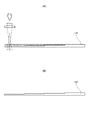
12,120−ガラス基板
14−アース導体部
16−アンテナ素子部
18−給電線
20−給電用貫通孔
24−ガラス母材
Claims (3)
- 誘電体基板としてガラス基板を用いるとともに、電波を受信するように構成された平面ガラスアンテナであって、
マトリックス状に配置された複数の給電用貫通孔を有するガラス基板と、
前記ガラス基板の第1の主面に設けられたアース導電部と、
前記ガラス基板の第2の主面における前記複数の給電用貫通孔にそれぞれ対応する位置に設けられた複数のアンテナ素子と、
を少なくとも備え、かつ、
前記ガラス基板は、前記アース導電部および前記アンテナ素子との間隔が異なる複数の領域が形成されるように、厚みの異なる複数の領域を有することを特徴とする平面ガラスアンテナ。 - 誘電体基板としてガラス基板を用いるとともに、電波を受信するように構成された平面ガラスアンテナを製造するための方法であって、
給電用貫通孔が形成されるべき位置にレーザビームを照射することによって、この位置にエッチングされやすい性質の改質部を形成する第1のレーザ加工ステップと、
前記改質部をエッチングすることによって給電用貫通孔を形成するエッチング処理ステップと、
を少なくとも含み、かつ、
前記エッチング処理ステップにおいて、フッ素錯化剤が添加されたエッチング液が用いられることを特徴とする平面ガラスアンテナの製造方法。 - 基板厚さが少なくとも2段階以上になるように、前記ガラス基板における薄型化すべき領域にレーザ焦点を調整しつつレーザビームを照射する第2のレーザ加工ステップをさらに含む請求項2に記載の平面ガラスアンテナ用ガラス基板の製造方法。
Priority Applications (3)
| Application Number | Priority Date | Filing Date | Title |
|---|---|---|---|
| JP2019097903A JP6840403B2 (ja) | 2019-05-24 | 2019-05-24 | 平面ガラスアンテナおよびその製造方法 |
| CN202080040767.0A CN113906630A (zh) | 2019-05-24 | 2020-05-19 | 平面玻璃天线及其制造方法 |
| PCT/JP2020/019735 WO2020241371A1 (ja) | 2019-05-24 | 2020-05-19 | 平面ガラスアンテナおよびその製造方法 |
Applications Claiming Priority (1)
| Application Number | Priority Date | Filing Date | Title |
|---|---|---|---|
| JP2019097903A JP6840403B2 (ja) | 2019-05-24 | 2019-05-24 | 平面ガラスアンテナおよびその製造方法 |
Publications (2)
| Publication Number | Publication Date |
|---|---|
| JP2020195002A JP2020195002A (ja) | 2020-12-03 |
| JP6840403B2 true JP6840403B2 (ja) | 2021-03-10 |
Family
ID=73547676
Family Applications (1)
| Application Number | Title | Priority Date | Filing Date |
|---|---|---|---|
| JP2019097903A Active JP6840403B2 (ja) | 2019-05-24 | 2019-05-24 | 平面ガラスアンテナおよびその製造方法 |
Country Status (3)
| Country | Link |
|---|---|
| JP (1) | JP6840403B2 (ja) |
| CN (1) | CN113906630A (ja) |
| WO (1) | WO2020241371A1 (ja) |
Cited By (1)
| Publication number | Priority date | Publication date | Assignee | Title |
|---|---|---|---|---|
| US12609433B2 (en) | 2021-08-06 | 2026-04-21 | Samsung Electronics Co., Ltd. | Electronic device including a semiconductor element on a glass substrate, where the semiconductor element is connected to a feed line by a second pattern and a via hole |
Families Citing this family (1)
| Publication number | Priority date | Publication date | Assignee | Title |
|---|---|---|---|---|
| KR102833259B1 (ko) * | 2020-08-13 | 2025-07-11 | 삼성디스플레이 주식회사 | 플렉서블 표시 장치용 커버 윈도우 제조 방법 및 플렉서블 표시 장치의 제조 방법 |
Family Cites Families (9)
| Publication number | Priority date | Publication date | Assignee | Title |
|---|---|---|---|---|
| JP2002171120A (ja) * | 2000-11-30 | 2002-06-14 | Asahi Glass Co Ltd | 電波収束構造体およびアンテナ装置 |
| JP2004304443A (ja) * | 2003-03-31 | 2004-10-28 | Clarion Co Ltd | アンテナ |
| EP1667509A4 (en) * | 2003-09-09 | 2009-05-20 | Hoya Corp | METHOD FOR MANUFACTURING A GLASS PLATE PRINTED ON BOTH SIDES |
| US8901688B2 (en) * | 2011-05-05 | 2014-12-02 | Intel Corporation | High performance glass-based 60 ghz / mm-wave phased array antennas and methods of making same |
| TWI461378B (zh) * | 2012-10-12 | 2014-11-21 | Global Display Co Ltd | 具波浪形表面之玻璃基板的製造方法 |
| US9472859B2 (en) * | 2014-05-20 | 2016-10-18 | International Business Machines Corporation | Integration of area efficient antennas for phased array or wafer scale array antenna applications |
| KR102337969B1 (ko) * | 2014-10-22 | 2021-12-09 | 닛본 이따 가라스 가부시끼가이샤 | 유리 기판의 제조 방법 및 판형상의 유리 |
| JP2018018891A (ja) * | 2016-07-26 | 2018-02-01 | 株式会社フジクラ | 配線基板およびその製造方法 |
| JP6803018B2 (ja) * | 2019-03-05 | 2020-12-23 | 株式会社Nsc | ガラス用エッチング液およびガラス基板製造方法 |
-
2019
- 2019-05-24 JP JP2019097903A patent/JP6840403B2/ja active Active
-
2020
- 2020-05-19 WO PCT/JP2020/019735 patent/WO2020241371A1/ja not_active Ceased
- 2020-05-19 CN CN202080040767.0A patent/CN113906630A/zh active Pending
Cited By (1)
| Publication number | Priority date | Publication date | Assignee | Title |
|---|---|---|---|---|
| US12609433B2 (en) | 2021-08-06 | 2026-04-21 | Samsung Electronics Co., Ltd. | Electronic device including a semiconductor element on a glass substrate, where the semiconductor element is connected to a feed line by a second pattern and a via hole |
Also Published As
| Publication number | Publication date |
|---|---|
| WO2020241371A1 (ja) | 2020-12-03 |
| JP2020195002A (ja) | 2020-12-03 |
| CN113906630A (zh) | 2022-01-07 |
Similar Documents
| Publication | Publication Date | Title |
|---|---|---|
| JP4340246B2 (ja) | 薄膜太陽電池およびその製造方法 | |
| US8421696B2 (en) | Dual polarization antenna structure, radome and design method thereof | |
| JP7723914B2 (ja) | 貫通電極基板、貫通電極基板を備える実装基板並びに貫通電極基板の製造方法 | |
| JP7264461B2 (ja) | 平面ガラスアンテナの製造方法。 | |
| JP6840403B2 (ja) | 平面ガラスアンテナおよびその製造方法 | |
| JP7279769B2 (ja) | 有孔基板及び実装基板 | |
| FR2984613A1 (fr) | Antenne imprimee optiquement transparente et reseau d'antennes optiquement transparentes | |
| CN114865301B (zh) | 一种宽频带太阳电池天线 | |
| WO2022071608A1 (ja) | 配線基板および配線基板の製造方法 | |
| CN109979318B (zh) | 显示母板及其制造和切割方法、显示基板及装置 | |
| Mias et al. | Optically transparent microstrip antennas | |
| KR20120125280A (ko) | 마스크 없이 oled 소자를 제조하는 방법 | |
| Deepa Nivethika et al. | A stretchable smart and highly efficient radio frequency antenna on low cost substrate | |
| EP2510563B1 (en) | Electro-optical device with electrode, and method of manufacturing the electro-optical device | |
| JP2021077717A (ja) | ガラス基板および導電パターンが設けられたガラス基板の製造方法 | |
| WO2019195806A3 (en) | Local patterning and metallization of semiconductor structures using a laser beam | |
| CN109037874B (zh) | 在石英电路上制作梁式引线的方法 | |
| JP2024178455A (ja) | 配線基板及び配線基板を備える実装基板並びに配線基板の製造方法 | |
| JP2019075626A (ja) | マイクロ波帯アンテナ | |
| JP7750366B2 (ja) | 導電基板およびその製造方法 | |
| JP2018125491A (ja) | 導電基板およびその製造方法 | |
| JP2007012730A (ja) | 光起電力装置およびその製造方法 | |
| JP7470950B2 (ja) | アンテナ及びその製造方法 | |
| JP7223352B2 (ja) | 導電基板およびその製造方法 | |
| US20060108336A1 (en) | Fabrication process for large-scale panel devices |
Legal Events
| Date | Code | Title | Description |
|---|---|---|---|
| A621 | Written request for application examination |
Free format text: JAPANESE INTERMEDIATE CODE: A621 Effective date: 20200519 |
|
| A131 | Notification of reasons for refusal |
Free format text: JAPANESE INTERMEDIATE CODE: A131 Effective date: 20200722 |
|
| A521 | Request for written amendment filed |
Free format text: JAPANESE INTERMEDIATE CODE: A523 Effective date: 20200911 |
|
| TRDD | Decision of grant or rejection written | ||
| A01 | Written decision to grant a patent or to grant a registration (utility model) |
Free format text: JAPANESE INTERMEDIATE CODE: A01 Effective date: 20210118 |
|
| A61 | First payment of annual fees (during grant procedure) |
Free format text: JAPANESE INTERMEDIATE CODE: A61 Effective date: 20210202 |
|
| R150 | Certificate of patent or registration of utility model |
Ref document number: 6840403 Country of ref document: JP Free format text: JAPANESE INTERMEDIATE CODE: R150 |
|
| R250 | Receipt of annual fees |
Free format text: JAPANESE INTERMEDIATE CODE: R250 |
|
| R250 | Receipt of annual fees |
Free format text: JAPANESE INTERMEDIATE CODE: R250 |
|
| R250 | Receipt of annual fees |
Free format text: JAPANESE INTERMEDIATE CODE: R250 |