JP6862529B2 - 表示装置 - Google Patents
表示装置 Download PDFInfo
- Publication number
- JP6862529B2 JP6862529B2 JP2019224158A JP2019224158A JP6862529B2 JP 6862529 B2 JP6862529 B2 JP 6862529B2 JP 2019224158 A JP2019224158 A JP 2019224158A JP 2019224158 A JP2019224158 A JP 2019224158A JP 6862529 B2 JP6862529 B2 JP 6862529B2
- Authority
- JP
- Japan
- Prior art keywords
- light emitting
- sub
- emitting layer
- light
- pixel
- Prior art date
- Legal status (The legal status is an assumption and is not a legal conclusion. Google has not performed a legal analysis and makes no representation as to the accuracy of the status listed.)
- Active
Links
Images


Classifications
-
- H—ELECTRICITY
- H10—SEMICONDUCTOR DEVICES; ELECTRIC SOLID-STATE DEVICES NOT OTHERWISE PROVIDED FOR
- H10K—ORGANIC ELECTRIC SOLID-STATE DEVICES
- H10K50/00—Organic light-emitting devices
- H10K50/10—OLEDs or polymer light-emitting diodes [PLED]
- H10K50/11—OLEDs or polymer light-emitting diodes [PLED] characterised by the electroluminescent [EL] layers
- H10K50/125—OLEDs or polymer light-emitting diodes [PLED] characterised by the electroluminescent [EL] layers specially adapted for multicolour light emission, e.g. for emitting white light
- H10K50/13—OLEDs or polymer light-emitting diodes [PLED] characterised by the electroluminescent [EL] layers specially adapted for multicolour light emission, e.g. for emitting white light comprising stacked EL layers within one EL unit
- H10K50/131—OLEDs or polymer light-emitting diodes [PLED] characterised by the electroluminescent [EL] layers specially adapted for multicolour light emission, e.g. for emitting white light comprising stacked EL layers within one EL unit with spacer layers between the electroluminescent layers
-
- H—ELECTRICITY
- H10—SEMICONDUCTOR DEVICES; ELECTRIC SOLID-STATE DEVICES NOT OTHERWISE PROVIDED FOR
- H10K—ORGANIC ELECTRIC SOLID-STATE DEVICES
- H10K59/00—Integrated devices, or assemblies of multiple devices, comprising at least one organic light-emitting element covered by group H10K50/00
- H10K59/30—Devices specially adapted for multicolour light emission
- H10K59/32—Stacked devices having two or more layers, each emitting at different wavelengths
-
- H—ELECTRICITY
- H10—SEMICONDUCTOR DEVICES; ELECTRIC SOLID-STATE DEVICES NOT OTHERWISE PROVIDED FOR
- H10K—ORGANIC ELECTRIC SOLID-STATE DEVICES
- H10K59/00—Integrated devices, or assemblies of multiple devices, comprising at least one organic light-emitting element covered by group H10K50/00
- H10K59/80—Constructional details
- H10K59/875—Arrangements for extracting light from the devices
-
- H—ELECTRICITY
- H10—SEMICONDUCTOR DEVICES; ELECTRIC SOLID-STATE DEVICES NOT OTHERWISE PROVIDED FOR
- H10K—ORGANIC ELECTRIC SOLID-STATE DEVICES
- H10K50/00—Organic light-emitting devices
- H10K50/10—OLEDs or polymer light-emitting diodes [PLED]
- H10K50/11—OLEDs or polymer light-emitting diodes [PLED] characterised by the electroluminescent [EL] layers
- H10K50/125—OLEDs or polymer light-emitting diodes [PLED] characterised by the electroluminescent [EL] layers specially adapted for multicolour light emission, e.g. for emitting white light
- H10K50/13—OLEDs or polymer light-emitting diodes [PLED] characterised by the electroluminescent [EL] layers specially adapted for multicolour light emission, e.g. for emitting white light comprising stacked EL layers within one EL unit
-
- H—ELECTRICITY
- H10—SEMICONDUCTOR DEVICES; ELECTRIC SOLID-STATE DEVICES NOT OTHERWISE PROVIDED FOR
- H10K—ORGANIC ELECTRIC SOLID-STATE DEVICES
- H10K50/00—Organic light-emitting devices
- H10K50/10—OLEDs or polymer light-emitting diodes [PLED]
- H10K50/19—Tandem OLEDs
-
- H—ELECTRICITY
- H10—SEMICONDUCTOR DEVICES; ELECTRIC SOLID-STATE DEVICES NOT OTHERWISE PROVIDED FOR
- H10K—ORGANIC ELECTRIC SOLID-STATE DEVICES
- H10K50/00—Organic light-emitting devices
- H10K50/80—Constructional details
- H10K50/85—Arrangements for extracting light from the devices
- H10K50/856—Arrangements for extracting light from the devices comprising reflective means
-
- H—ELECTRICITY
- H10—SEMICONDUCTOR DEVICES; ELECTRIC SOLID-STATE DEVICES NOT OTHERWISE PROVIDED FOR
- H10K—ORGANIC ELECTRIC SOLID-STATE DEVICES
- H10K59/00—Integrated devices, or assemblies of multiple devices, comprising at least one organic light-emitting element covered by group H10K50/00
- H10K59/10—OLED displays
- H10K59/12—Active-matrix OLED [AMOLED] displays
- H10K59/122—Pixel-defining structures or layers, e.g. banks
-
- H—ELECTRICITY
- H10—SEMICONDUCTOR DEVICES; ELECTRIC SOLID-STATE DEVICES NOT OTHERWISE PROVIDED FOR
- H10K—ORGANIC ELECTRIC SOLID-STATE DEVICES
- H10K59/00—Integrated devices, or assemblies of multiple devices, comprising at least one organic light-emitting element covered by group H10K50/00
- H10K59/10—OLED displays
- H10K59/12—Active-matrix OLED [AMOLED] displays
- H10K59/123—Connection of the pixel electrodes to the thin film transistors [TFT]
-
- H—ELECTRICITY
- H10—SEMICONDUCTOR DEVICES; ELECTRIC SOLID-STATE DEVICES NOT OTHERWISE PROVIDED FOR
- H10K—ORGANIC ELECTRIC SOLID-STATE DEVICES
- H10K59/00—Integrated devices, or assemblies of multiple devices, comprising at least one organic light-emitting element covered by group H10K50/00
- H10K59/10—OLED displays
- H10K59/12—Active-matrix OLED [AMOLED] displays
- H10K59/131—Interconnections, e.g. wiring lines or terminals
-
- H—ELECTRICITY
- H10—SEMICONDUCTOR DEVICES; ELECTRIC SOLID-STATE DEVICES NOT OTHERWISE PROVIDED FOR
- H10K—ORGANIC ELECTRIC SOLID-STATE DEVICES
- H10K59/00—Integrated devices, or assemblies of multiple devices, comprising at least one organic light-emitting element covered by group H10K50/00
- H10K59/30—Devices specially adapted for multicolour light emission
- H10K59/35—Devices specially adapted for multicolour light emission comprising red-green-blue [RGB] subpixels
-
- H—ELECTRICITY
- H10—SEMICONDUCTOR DEVICES; ELECTRIC SOLID-STATE DEVICES NOT OTHERWISE PROVIDED FOR
- H10K—ORGANIC ELECTRIC SOLID-STATE DEVICES
- H10K59/00—Integrated devices, or assemblies of multiple devices, comprising at least one organic light-emitting element covered by group H10K50/00
- H10K59/30—Devices specially adapted for multicolour light emission
- H10K59/38—Devices specially adapted for multicolour light emission comprising colour filters or colour changing media [CCM]
-
- H—ELECTRICITY
- H10—SEMICONDUCTOR DEVICES; ELECTRIC SOLID-STATE DEVICES NOT OTHERWISE PROVIDED FOR
- H10K—ORGANIC ELECTRIC SOLID-STATE DEVICES
- H10K59/00—Integrated devices, or assemblies of multiple devices, comprising at least one organic light-emitting element covered by group H10K50/00
- H10K59/80—Constructional details
- H10K59/805—Electrodes
-
- H—ELECTRICITY
- H10—SEMICONDUCTOR DEVICES; ELECTRIC SOLID-STATE DEVICES NOT OTHERWISE PROVIDED FOR
- H10K—ORGANIC ELECTRIC SOLID-STATE DEVICES
- H10K59/00—Integrated devices, or assemblies of multiple devices, comprising at least one organic light-emitting element covered by group H10K50/00
- H10K59/80—Constructional details
- H10K59/875—Arrangements for extracting light from the devices
- H10K59/878—Arrangements for extracting light from the devices comprising reflective means
-
- H—ELECTRICITY
- H10—SEMICONDUCTOR DEVICES; ELECTRIC SOLID-STATE DEVICES NOT OTHERWISE PROVIDED FOR
- H10K—ORGANIC ELECTRIC SOLID-STATE DEVICES
- H10K59/00—Integrated devices, or assemblies of multiple devices, comprising at least one organic light-emitting element covered by group H10K50/00
- H10K59/80—Constructional details
- H10K59/875—Arrangements for extracting light from the devices
- H10K59/879—Arrangements for extracting light from the devices comprising refractive means, e.g. lenses
-
- G—PHYSICS
- G02—OPTICS
- G02B—OPTICAL ELEMENTS, SYSTEMS OR APPARATUS
- G02B27/00—Optical systems or apparatus not provided for by any of the groups G02B1/00 - G02B26/00, G02B30/00
- G02B27/01—Head-up displays
- G02B27/0101—Head-up displays characterised by optical features
- G02B2027/0112—Head-up displays characterised by optical features comprising device for genereting colour display
-
- G—PHYSICS
- G02—OPTICS
- G02B—OPTICAL ELEMENTS, SYSTEMS OR APPARATUS
- G02B27/00—Optical systems or apparatus not provided for by any of the groups G02B1/00 - G02B26/00, G02B30/00
- G02B27/01—Head-up displays
- G02B27/017—Head mounted
- G02B27/0172—Head mounted characterised by optical features
-
- G—PHYSICS
- G06—COMPUTING OR CALCULATING; COUNTING
- G06F—ELECTRIC DIGITAL DATA PROCESSING
- G06F1/00—Details not covered by groups G06F3/00 - G06F13/00 and G06F21/00
- G06F1/16—Constructional details or arrangements
- G06F1/1613—Constructional details or arrangements for portable computers
- G06F1/163—Wearable computers, e.g. on a belt
-
- H—ELECTRICITY
- H10—SEMICONDUCTOR DEVICES; ELECTRIC SOLID-STATE DEVICES NOT OTHERWISE PROVIDED FOR
- H10K—ORGANIC ELECTRIC SOLID-STATE DEVICES
- H10K2102/00—Constructional details relating to the organic devices covered by this subclass
- H10K2102/301—Details of OLEDs
- H10K2102/302—Details of OLEDs of OLED structures
- H10K2102/3023—Direction of light emission
- H10K2102/3026—Top emission
-
- H—ELECTRICITY
- H10—SEMICONDUCTOR DEVICES; ELECTRIC SOLID-STATE DEVICES NOT OTHERWISE PROVIDED FOR
- H10K—ORGANIC ELECTRIC SOLID-STATE DEVICES
- H10K2102/00—Constructional details relating to the organic devices covered by this subclass
- H10K2102/301—Details of OLEDs
- H10K2102/302—Details of OLEDs of OLED structures
- H10K2102/3023—Direction of light emission
- H10K2102/3035—Edge emission
Landscapes
- Engineering & Computer Science (AREA)
- Microelectronics & Electronic Packaging (AREA)
- Physics & Mathematics (AREA)
- Optics & Photonics (AREA)
- Electroluminescent Light Sources (AREA)
- Devices For Indicating Variable Information By Combining Individual Elements (AREA)
Description
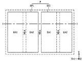
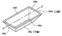
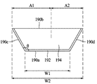
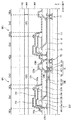
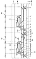
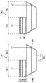
図4は、サブ画素の光ガイド構造物、第1電極、第2電極及び第3電極を概略的に示した平面図であり、図5は、図3のI−Iの第1例を示す断面図である。図6aは、図5に示した光ガイド構造物を概略的に示す斜視図であり、図6bは、図6aに示した光ガイド構造物のII―II線の断面図である。図7は図5の第1サブ画素および第2サブ画素で光の経路を概略的に示す図である。図8は、図5の変形された実施例を示す断面図であり、図9は、図5の他の変形された実施例を示す断面図であり、図10は、図5のまた他の変形された実施例を示す断面図である。
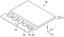
110:表示パネル
111:第1基板
112:第2基板
140:ソースドライブIC
150:軟性フィルム
160:回路基板
170:タイミング制御部
180:電源ライン
190:光ガイド構造物
210:第1電極
220:第1発光層
230:第2電極
240:第2発光層
250:第3電極
300:封止層
400:カラーフィルタ層
Claims (17)
- 第1サブ画素および第2サブ画素を有する複数の画素を備えた基板であって、
前記第1サブ画素および前記第2サブ画素の各々が、
第1発光領域および第2発光領域と、
前記第1発光領域に備えられた第1電極と、
前記第1電極上に備えられた第1発光層と、
前記第1発光層上に備えられた第2電極と、
前記第2電極上に備えられた第2発光層と、
前記第2発光層上に備えられた第3電極と
を含み、
前記第3電極は透明電極であり、
前記第1発光領域において、前記基板と前記第1電極の間に備えられ前記第2発光領域まで延長され、前記第1発光領域に備えられた前記第1発光層で発光した光を前記第2発光領域にガイドする光ガイド構造物を含む表示装置。 - 前記第2電極が、反射電極であり、前記第1電極は、透明電極である請求項1に記載の表示装置。
- 前記第2電極が、前記第1発光層で発光した光を前記光ガイド構造物の方向に反射させ、
前記第2電極が、前記第2発光層で発光した光を前記第3電極の方向に反射させる請求項2に記載の表示装置。 - 前記光ガイド構造物が、第1幅を有する下面、前記第1幅よりも大きい第2幅を有する上面、前記下面と前記上面を連結する第1傾斜面と第2傾斜面を含む請求項1に記載の表示装置。
- 前記光ガイド構造物が、前記第1電極と重畳する第1領域および前記第1電極と重畳しない第2領域を含む請求項1に記載の表示装置。
- 前記光ガイド構造物が、反射空間を形成し、前記第1発光層から発光した光を反射させて前記第2発光領域にガイドする反射体を含む請求項4に記載の表示装置。
- 前記基板上に備えられた第1駆動薄膜トランジスタをさらに含み、
前記光ガイド構造物の反射体が、前記第1電極と前記第1駆動薄膜トランジスタのソース電極またはドレイン電極を電気的に接続する請求項6に記載の表示装置。 - 前記基板上に備えられた第2駆動薄膜トランジスタをさらに含み、
前記第3電極が、前記第2駆動薄膜トランジスタのソース電極またはドレイン電極に接続する請求項1に記載の表示装置。 - 前記第1サブ画素に備えられた第3電極と前記第2サブ画素に備えられた第3電極が、互いに接続し、一つの第2駆動薄膜トランジスタは、前記第1および第2サブ画素に共通に備えられる請求項8に記載の表示装置。
- 前記第3電極が、一つの画素の前記第1サブ画素及び前記第2サブ画素の各々に別途に備えられ、前記第1サブ画素及び前記第2サブ画素各々の第3電極は、各々の第2駆動薄膜トランジスタに接続している請求項8に記載の表示装置。
- 一つのサブ画素の前記第1発光層と前記第2発光層が、異なる色の波長帯の光を発光する請求項1に記載の表示装置。
- 前記各画素において、
前記第1サブ画素の第1発光領域と前記第2サブ画素の第1発光領域が、第1色波長帯の光を放出するように構成され、前記第1サブ画素の第2発光領域は、第2色波長帯の光を放出するように構成され、前記第2サブ画素の第2発光領域は、第3色波長帯の光を放出するように構成するか、
前記第1サブ画素の第2発光領域と前記第2サブ画素の第2発光領域が、第1色波長帯の光を放出するように構成され、前記第2サブ画素の第1発光領域は、第2色波長帯の光を放出するように構成され、前記第2サブ画素の第1発光領域は、第3色波長帯の光を放出するように構成され、
前記第1、第2および第3色波長帯は、互いに異なる請求項1に記載の表示装置。 - 前記各サブ画素が、前記第2発光領域に備えられたカラーフィルタをさらに含み、
前記カラーフィルタは、前記第1発光層から発光した光の一部のみを放出する請求項1に記載の表示装置。 - 前記各画素において、
前記第1サブ画素が、第1色波長帯の光及び第3色波長帯の光を放出するように構成され、前記第2サブ画素は、第2色波長帯の光及び第3色波長帯の光を放出するように構成され、前記第1、第2および第3色波長帯は、互いに異なる請求項1に記載の表示装置。 - 前記各画素において、
前記第1サブ画素の第1発光層と前記第2サブ画素の第1発光層が、同一な物質からなり同一な波長帯の光を放出するように構成され、前記第1サブ画素の第2発光層と前記第2サブ画素の第2発光層は、互いに異なる物質からなり、異なる色の波長帯の光を放出するように構成するか、
前記第1サブ画素の第1発光層と前記第2サブ画素の第1発光層が、互いに異なる物質からなり、異なる波長帯の光を放出するように構成され、前記第1サブ画素の第2発光層と前記第2サブ画素の第2発光層は、同一な物質からなり同一な色の波長帯の光を放出するように構成するか、
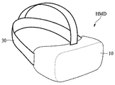
前記第1サブ画素の第1発光層と前記第2サブ画素の第1発光層が、同一な物質からなり同一な波長帯の光を放出するように構成され、前記第1サブ画素の第2発光層と前記第2サブ画素の第2発光層は、同一な物質からなり同一な色の波長帯の光を放出するように構成される請求項1に記載の表示装置。 - 収納ケースと、
前記収納ケースに固定されたヘッド装着バンドと
を含み、
前記収納ケースは、請求項1〜請求項15のいずれか一項による表示装置、接眼レンズ及び前記表示装置と前記接眼レンズとの間に配置されたレンズアレイを収納する、ヘッドマウントディスプレイ。 - 前記接眼レンズが、右眼接眼レンズおよび左眼接眼レンズを含み、前記表示装置は、右眼用表示装置と左眼用表示装置を含む請求項16に記載のヘッドマウントディスプレイ。
Applications Claiming Priority (2)
| Application Number | Priority Date | Filing Date | Title |
|---|---|---|---|
| KR1020180167953A KR102735978B1 (ko) | 2018-12-21 | 2018-12-21 | 표시장치 |
| KR10-2018-0167953 | 2018-12-21 |
Publications (2)
| Publication Number | Publication Date |
|---|---|
| JP2020102447A JP2020102447A (ja) | 2020-07-02 |
| JP6862529B2 true JP6862529B2 (ja) | 2021-04-21 |
Family
ID=68841032
Family Applications (1)
| Application Number | Title | Priority Date | Filing Date |
|---|---|---|---|
| JP2019224158A Active JP6862529B2 (ja) | 2018-12-21 | 2019-12-12 | 表示装置 |
Country Status (5)
| Country | Link |
|---|---|
| US (1) | US11398619B2 (ja) |
| EP (1) | EP3671880B1 (ja) |
| JP (1) | JP6862529B2 (ja) |
| KR (1) | KR102735978B1 (ja) |
| CN (1) | CN111354858B (ja) |
Families Citing this family (8)
| Publication number | Priority date | Publication date | Assignee | Title |
|---|---|---|---|---|
| KR20200119946A (ko) * | 2019-04-10 | 2020-10-21 | 삼성디스플레이 주식회사 | 표시 장치 |
| KR102682775B1 (ko) | 2020-06-26 | 2024-07-08 | 홀로스메딕 주식회사 | 신규한 화합물의 제조방법 |
| KR102870627B1 (ko) * | 2020-10-22 | 2025-10-14 | 엘지디스플레이 주식회사 | 전계 발광 표시장치 |
| CN112909053A (zh) * | 2021-01-26 | 2021-06-04 | 京东方科技集团股份有限公司 | 显示装置、显示面板及其制造方法 |
| KR102848809B1 (ko) | 2021-04-22 | 2025-08-25 | 삼성디스플레이 주식회사 | 표시 장치 및 표시 장치의 제조 방법 |
| JP7564966B2 (ja) * | 2021-10-13 | 2024-10-09 | シャープ株式会社 | 発光素子および発光デバイス |
| KR20240052519A (ko) * | 2022-10-14 | 2024-04-23 | 엘지디스플레이 주식회사 | 표시장치 |
| CN120769661A (zh) * | 2024-03-27 | 2025-10-10 | 荣耀终端股份有限公司 | 显示面板及其驱动方法、制作方法和电子设备 |
Family Cites Families (16)
| Publication number | Priority date | Publication date | Assignee | Title |
|---|---|---|---|---|
| JP2002313553A (ja) * | 2001-04-06 | 2002-10-25 | Kansai Tlo Kk | 高速動作有機el素子 |
| JP2004235019A (ja) * | 2003-01-30 | 2004-08-19 | Hitachi Displays Ltd | 有機発光表示装置 |
| TWI239221B (en) * | 2004-07-15 | 2005-09-01 | Ritdisplay Corp | Organic light-emitting source |
| JP2008233113A (ja) * | 2005-11-17 | 2008-10-02 | Toyota Industries Corp | 表示装置 |
| JP4899849B2 (ja) * | 2006-12-14 | 2012-03-21 | カシオ計算機株式会社 | 発光装置及び印刷装置 |
| CA2686174A1 (en) * | 2009-12-01 | 2011-06-01 | Ignis Innovation Inc | High reslution pixel architecture |
| WO2012108142A1 (ja) * | 2011-02-07 | 2012-08-16 | シャープ株式会社 | 有機el表示装置及びその製造方法 |
| KR101884199B1 (ko) * | 2011-06-29 | 2018-08-02 | 삼성디스플레이 주식회사 | 발광 구조물, 발광 구조물을 포함하는 표시 장치 및 표시 장치의 제조 방법 |
| KR102056466B1 (ko) * | 2013-06-04 | 2019-12-17 | 삼성디스플레이 주식회사 | 유기 발광 표시장치 및 그 제조방법 |
| JP6357349B2 (ja) * | 2014-05-16 | 2018-07-11 | 株式会社ジャパンディスプレイ | 表示装置 |
| TWI542066B (zh) * | 2014-06-10 | 2016-07-11 | 群創光電股份有限公司 | 有機發光二極體顯示器 |
| JP2016207740A (ja) * | 2015-04-17 | 2016-12-08 | 三菱化学株式会社 | 二面発光装置 |
| JP6812185B2 (ja) * | 2016-09-29 | 2021-01-13 | 株式会社ジャパンディスプレイ | 有機el表示装置 |
| KR102801173B1 (ko) * | 2016-10-31 | 2025-04-25 | 엘지디스플레이 주식회사 | 유기발광 표시장치와 그의 제조방법 |
| KR102663231B1 (ko) * | 2016-12-30 | 2024-05-02 | 엘지디스플레이 주식회사 | 유기발광 표시장치 |
| KR102737176B1 (ko) * | 2017-01-31 | 2024-12-04 | 삼성디스플레이 주식회사 | 표시 기판 및 이를 포함하는 표시 장치 |
-
2018
- 2018-12-21 KR KR1020180167953A patent/KR102735978B1/ko active Active
-
2019
- 2019-11-29 CN CN201911199535.5A patent/CN111354858B/zh active Active
- 2019-12-10 EP EP19214644.7A patent/EP3671880B1/en active Active
- 2019-12-12 JP JP2019224158A patent/JP6862529B2/ja active Active
- 2019-12-20 US US16/722,735 patent/US11398619B2/en active Active
Also Published As
| Publication number | Publication date |
|---|---|
| EP3671880B1 (en) | 2021-11-17 |
| EP3671880A1 (en) | 2020-06-24 |
| CN111354858B (zh) | 2023-03-24 |
| KR20200078242A (ko) | 2020-07-01 |
| CN111354858A (zh) | 2020-06-30 |
| US11398619B2 (en) | 2022-07-26 |
| KR102735978B1 (ko) | 2024-11-28 |
| JP2020102447A (ja) | 2020-07-02 |
| US20200203667A1 (en) | 2020-06-25 |
Similar Documents
| Publication | Publication Date | Title |
|---|---|---|
| JP6862529B2 (ja) | 表示装置 | |
| US10677968B2 (en) | Display device method for manufacturing the same and head mounted display during the same | |
| JP6990680B2 (ja) | 表示装置 | |
| KR102735986B1 (ko) | 표시장치 | |
| JP6605441B2 (ja) | 表示装置及びその製造方法 | |
| US11917846B2 (en) | Display device having an oxide insulating film between subpixels and method for manufacturing the same | |
| KR102630000B1 (ko) | 표시장치 | |
| KR20180002471A (ko) | 유기발광 표시장치, 그의 제조방법, 및 그를 포함한 헤드 장착형 디스플레이 | |
| US12364151B2 (en) | Display device, method of manufacturing display device, electronic apparatus, and lighting device | |
| WO2022259919A1 (ja) | 発光装置及び電子機器 | |
| KR102719992B1 (ko) | 표시장치 | |
| US20240423071A1 (en) | Display device and electronic apparatus | |
| US11114467B2 (en) | Display device | |
| KR102844129B1 (ko) | 표시장치 | |
| US20260047302A1 (en) | Light emitting device and electronic apparatus | |
| GB2588295A (en) | Display device and method for manufacturing the same | |
| KR20260048727A (ko) | 표시 장치 | |
| KR20210053654A (ko) | 표시장치 |
Legal Events
| Date | Code | Title | Description |
|---|---|---|---|
| A621 | Written request for application examination |
Free format text: JAPANESE INTERMEDIATE CODE: A621 Effective date: 20191212 |
|
| A131 | Notification of reasons for refusal |
Free format text: JAPANESE INTERMEDIATE CODE: A131 Effective date: 20201119 |
|
| A977 | Report on retrieval |
Free format text: JAPANESE INTERMEDIATE CODE: A971007 Effective date: 20201130 |
|
| A521 | Request for written amendment filed |
Free format text: JAPANESE INTERMEDIATE CODE: A523 Effective date: 20210219 |
|
| TRDD | Decision of grant or rejection written | ||
| A01 | Written decision to grant a patent or to grant a registration (utility model) |
Free format text: JAPANESE INTERMEDIATE CODE: A01 Effective date: 20210304 |
|
| A61 | First payment of annual fees (during grant procedure) |
Free format text: JAPANESE INTERMEDIATE CODE: A61 Effective date: 20210331 |
|
| R150 | Certificate of patent or registration of utility model |
Ref document number: 6862529 Country of ref document: JP Free format text: JAPANESE INTERMEDIATE CODE: R150 |
|
| R250 | Receipt of annual fees |
Free format text: JAPANESE INTERMEDIATE CODE: R250 |
|
| R250 | Receipt of annual fees |
Free format text: JAPANESE INTERMEDIATE CODE: R250 |
|
| R250 | Receipt of annual fees |
Free format text: JAPANESE INTERMEDIATE CODE: R250 |