JP6875808B2 - 情報処理装置 - Google Patents
情報処理装置 Download PDFInfo
- Publication number
- JP6875808B2 JP6875808B2 JP2016177141A JP2016177141A JP6875808B2 JP 6875808 B2 JP6875808 B2 JP 6875808B2 JP 2016177141 A JP2016177141 A JP 2016177141A JP 2016177141 A JP2016177141 A JP 2016177141A JP 6875808 B2 JP6875808 B2 JP 6875808B2
- Authority
- JP
- Japan
- Prior art keywords
- storage device
- erasing
- information processing
- command
- data
- Prior art date
- Legal status (The legal status is an assumption and is not a legal conclusion. Google has not performed a legal analysis and makes no representation as to the accuracy of the status listed.)
- Active
Links
Images



Classifications
-
- G—PHYSICS
- G06—COMPUTING OR CALCULATING; COUNTING
- G06F—ELECTRIC DIGITAL DATA PROCESSING
- G06F3/00—Input arrangements for transferring data to be processed into a form capable of being handled by the computer; Output arrangements for transferring data from processing unit to output unit, e.g. interface arrangements
- G06F3/12—Digital output to print unit, e.g. line printer, chain printer
- G06F3/1201—Dedicated interfaces to print systems
- G06F3/1223—Dedicated interfaces to print systems specifically adapted to use a particular technique
- G06F3/1237—Print job management
- G06F3/1274—Deleting of print job
-
- G—PHYSICS
- G06—COMPUTING OR CALCULATING; COUNTING
- G06F—ELECTRIC DIGITAL DATA PROCESSING
- G06F3/00—Input arrangements for transferring data to be processed into a form capable of being handled by the computer; Output arrangements for transferring data from processing unit to output unit, e.g. interface arrangements
- G06F3/06—Digital input from, or digital output to, record carriers, e.g. RAID, emulated record carriers or networked record carriers
- G06F3/0601—Interfaces specially adapted for storage systems
- G06F3/0628—Interfaces specially adapted for storage systems making use of a particular technique
- G06F3/0646—Horizontal data movement in storage systems, i.e. moving data in between storage devices or systems
- G06F3/0652—Erasing, e.g. deleting, data cleaning, moving of data to a wastebasket
-
- G—PHYSICS
- G06—COMPUTING OR CALCULATING; COUNTING
- G06F—ELECTRIC DIGITAL DATA PROCESSING
- G06F3/00—Input arrangements for transferring data to be processed into a form capable of being handled by the computer; Output arrangements for transferring data from processing unit to output unit, e.g. interface arrangements
- G06F3/06—Digital input from, or digital output to, record carriers, e.g. RAID, emulated record carriers or networked record carriers
- G06F3/0601—Interfaces specially adapted for storage systems
- G06F3/0602—Interfaces specially adapted for storage systems specifically adapted to achieve a particular effect
- G06F3/0604—Improving or facilitating administration, e.g. storage management
- G06F3/0605—Improving or facilitating administration, e.g. storage management by facilitating the interaction with a user or administrator
-
- G—PHYSICS
- G06—COMPUTING OR CALCULATING; COUNTING
- G06F—ELECTRIC DIGITAL DATA PROCESSING
- G06F3/00—Input arrangements for transferring data to be processed into a form capable of being handled by the computer; Output arrangements for transferring data from processing unit to output unit, e.g. interface arrangements
- G06F3/06—Digital input from, or digital output to, record carriers, e.g. RAID, emulated record carriers or networked record carriers
- G06F3/0601—Interfaces specially adapted for storage systems
- G06F3/0602—Interfaces specially adapted for storage systems specifically adapted to achieve a particular effect
- G06F3/0608—Saving storage space on storage systems
-
- G—PHYSICS
- G06—COMPUTING OR CALCULATING; COUNTING
- G06F—ELECTRIC DIGITAL DATA PROCESSING
- G06F3/00—Input arrangements for transferring data to be processed into a form capable of being handled by the computer; Output arrangements for transferring data from processing unit to output unit, e.g. interface arrangements
- G06F3/06—Digital input from, or digital output to, record carriers, e.g. RAID, emulated record carriers or networked record carriers
- G06F3/0601—Interfaces specially adapted for storage systems
- G06F3/0628—Interfaces specially adapted for storage systems making use of a particular technique
- G06F3/0653—Monitoring storage devices or systems
-
- G—PHYSICS
- G06—COMPUTING OR CALCULATING; COUNTING
- G06F—ELECTRIC DIGITAL DATA PROCESSING
- G06F3/00—Input arrangements for transferring data to be processed into a form capable of being handled by the computer; Output arrangements for transferring data from processing unit to output unit, e.g. interface arrangements
- G06F3/06—Digital input from, or digital output to, record carriers, e.g. RAID, emulated record carriers or networked record carriers
- G06F3/0601—Interfaces specially adapted for storage systems
- G06F3/0668—Interfaces specially adapted for storage systems adopting a particular infrastructure
- G06F3/0671—In-line storage system
- G06F3/0673—Single storage device
-
- G—PHYSICS
- G06—COMPUTING OR CALCULATING; COUNTING
- G06F—ELECTRIC DIGITAL DATA PROCESSING
- G06F3/00—Input arrangements for transferring data to be processed into a form capable of being handled by the computer; Output arrangements for transferring data from processing unit to output unit, e.g. interface arrangements
- G06F3/06—Digital input from, or digital output to, record carriers, e.g. RAID, emulated record carriers or networked record carriers
- G06F3/0601—Interfaces specially adapted for storage systems
- G06F3/0668—Interfaces specially adapted for storage systems adopting a particular infrastructure
- G06F3/0671—In-line storage system
- G06F3/0673—Single storage device
- G06F3/0679—Non-volatile semiconductor memory device, e.g. flash memory, one time programmable memory [OTP]
-
- G—PHYSICS
- G06—COMPUTING OR CALCULATING; COUNTING
- G06F—ELECTRIC DIGITAL DATA PROCESSING
- G06F3/00—Input arrangements for transferring data to be processed into a form capable of being handled by the computer; Output arrangements for transferring data from processing unit to output unit, e.g. interface arrangements
- G06F3/06—Digital input from, or digital output to, record carriers, e.g. RAID, emulated record carriers or networked record carriers
- G06F3/0601—Interfaces specially adapted for storage systems
- G06F3/0668—Interfaces specially adapted for storage systems adopting a particular infrastructure
- G06F3/0671—In-line storage system
- G06F3/0673—Single storage device
- G06F3/068—Hybrid storage device
-
- G—PHYSICS
- G06—COMPUTING OR CALCULATING; COUNTING
- G06F—ELECTRIC DIGITAL DATA PROCESSING
- G06F3/00—Input arrangements for transferring data to be processed into a form capable of being handled by the computer; Output arrangements for transferring data from processing unit to output unit, e.g. interface arrangements
- G06F3/12—Digital output to print unit, e.g. line printer, chain printer
- G06F3/1201—Dedicated interfaces to print systems
- G06F3/1202—Dedicated interfaces to print systems specifically adapted to achieve a particular effect
- G06F3/1203—Improving or facilitating administration, e.g. print management
- G06F3/1205—Improving or facilitating administration, e.g. print management resulting in increased flexibility in print job configuration, e.g. job settings, print requirements, job tickets
-
- G—PHYSICS
- G06—COMPUTING OR CALCULATING; COUNTING
- G06F—ELECTRIC DIGITAL DATA PROCESSING
- G06F3/00—Input arrangements for transferring data to be processed into a form capable of being handled by the computer; Output arrangements for transferring data from processing unit to output unit, e.g. interface arrangements
- G06F3/12—Digital output to print unit, e.g. line printer, chain printer
- G06F3/1201—Dedicated interfaces to print systems
- G06F3/1202—Dedicated interfaces to print systems specifically adapted to achieve a particular effect
- G06F3/1203—Improving or facilitating administration, e.g. print management
- G06F3/1207—Improving or facilitating administration, e.g. print management resulting in the user being informed about print result after a job submission
-
- G—PHYSICS
- G06—COMPUTING OR CALCULATING; COUNTING
- G06F—ELECTRIC DIGITAL DATA PROCESSING
- G06F3/00—Input arrangements for transferring data to be processed into a form capable of being handled by the computer; Output arrangements for transferring data from processing unit to output unit, e.g. interface arrangements
- G06F3/12—Digital output to print unit, e.g. line printer, chain printer
- G06F3/1201—Dedicated interfaces to print systems
- G06F3/1202—Dedicated interfaces to print systems specifically adapted to achieve a particular effect
- G06F3/1218—Reducing or saving of used resources, e.g. avoiding waste of consumables or improving usage of hardware resources
- G06F3/122—Reducing or saving of used resources, e.g. avoiding waste of consumables or improving usage of hardware resources with regard to computing resources, e.g. memory, CPU
-
- G—PHYSICS
- G06—COMPUTING OR CALCULATING; COUNTING
- G06F—ELECTRIC DIGITAL DATA PROCESSING
- G06F3/00—Input arrangements for transferring data to be processed into a form capable of being handled by the computer; Output arrangements for transferring data from processing unit to output unit, e.g. interface arrangements
- G06F3/12—Digital output to print unit, e.g. line printer, chain printer
- G06F3/1201—Dedicated interfaces to print systems
- G06F3/1202—Dedicated interfaces to print systems specifically adapted to achieve a particular effect
- G06F3/1222—Increasing security of the print job
-
- G—PHYSICS
- G06—COMPUTING OR CALCULATING; COUNTING
- G06F—ELECTRIC DIGITAL DATA PROCESSING
- G06F3/00—Input arrangements for transferring data to be processed into a form capable of being handled by the computer; Output arrangements for transferring data from processing unit to output unit, e.g. interface arrangements
- G06F3/12—Digital output to print unit, e.g. line printer, chain printer
- G06F3/1201—Dedicated interfaces to print systems
- G06F3/1223—Dedicated interfaces to print systems specifically adapted to use a particular technique
- G06F3/1229—Printer resources management or printer maintenance, e.g. device status, power levels
- G06F3/1231—Device related settings, e.g. IP address, Name, Identification
-
- G—PHYSICS
- G06—COMPUTING OR CALCULATING; COUNTING
- G06F—ELECTRIC DIGITAL DATA PROCESSING
- G06F3/00—Input arrangements for transferring data to be processed into a form capable of being handled by the computer; Output arrangements for transferring data from processing unit to output unit, e.g. interface arrangements
- G06F3/12—Digital output to print unit, e.g. line printer, chain printer
- G06F3/1201—Dedicated interfaces to print systems
- G06F3/1278—Dedicated interfaces to print systems specifically adapted to adopt a particular infrastructure
- G06F3/1285—Remote printer device, e.g. being remote from client or server
-
- G—PHYSICS
- G06—COMPUTING OR CALCULATING; COUNTING
- G06F—ELECTRIC DIGITAL DATA PROCESSING
- G06F3/00—Input arrangements for transferring data to be processed into a form capable of being handled by the computer; Output arrangements for transferring data from processing unit to output unit, e.g. interface arrangements
- G06F3/06—Digital input from, or digital output to, record carriers, e.g. RAID, emulated record carriers or networked record carriers
- G06F3/0601—Interfaces specially adapted for storage systems
- G06F3/0602—Interfaces specially adapted for storage systems specifically adapted to achieve a particular effect
- G06F3/062—Securing storage systems
- G06F3/0623—Securing storage systems in relation to content
Landscapes
- Engineering & Computer Science (AREA)
- Theoretical Computer Science (AREA)
- Physics & Mathematics (AREA)
- Human Computer Interaction (AREA)
- General Engineering & Computer Science (AREA)
- General Physics & Mathematics (AREA)
- Mathematical Physics (AREA)
- Computer Security & Cryptography (AREA)
- Facsimiles In General (AREA)
- Storing Facsimile Image Data (AREA)
- Accessory Devices And Overall Control Thereof (AREA)
- Storage Device Security (AREA)
- User Interface Of Digital Computer (AREA)
Description
第1実施形態では、情報処理装置の一例として、印刷機能、複写機能、画像送信機能、画像保存機能等の多数の機能を有する画像形成装置(画像処理装置)である複合機(MFP)について説明する。なお、本実施形態は、MFPだけでなく、印刷装置(プリンタ)、複写機、ファクシミリ装置、PC等の情報処理装置にも同様に適用可能である。
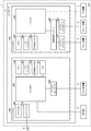
図1は、本実施形態に係るMFP1の構成例を示すブロック図である。MFP1は、コントローラ3と、コントローラ3に接続されたスキャナ装置2、プリンタ装置4、操作部5、二次記憶装置6、及びFAX(ファクシミリ)装置7とを備える。スキャナ装置2は、原稿から光学的に画像を読み取って当該画像をデジタル画像に変換し、画像データとして出力する。プリンタ装置4は、画像データに基づいてシート(記録紙等)に画像を印刷する。操作部5は、操作ボタン、及びタッチパネル機能を有する表示パネルを備え、MFP1に対するユーザの操作を受け付けるために用いられるとともに、及び各種情報及び操作画面の表示のために用いられる。FAX装置7は、電話回線を介したFAX送信により、指定された宛先に画像データを送信する。
ここで、二次記憶装置6としてMFP1に搭載可能なSSDにおけるデータの消去処理について説明する。SSDは、ページと称される単位とブロックと称される単位で、記憶領域内のデータを管理する。ページは、書き込み処理または読み出し処理の最小単位であり、通常数Kバイトを有する。ブロックは、消去処理の単位であり、複数のページで構成される。SSDでは、データを書き込み済みのページに直接的に上書きはできず、データの書き込み前に、対象となるページに書き込み済みのデータの消去処理を行う必要がある。この消去処理は、ページ単位でなく、データの削除単位であるブロック単位で行う必要がある。このため、書き込み可能なページ(即ち、データを消去済みのページ)が存在しない状態においてデータの書き込み処理を行う際には、書き込み処理に先立ってブロック単位でのデータの消去処理を行う。
次に、図8を参照して、二次記憶装置6としてSSDがMFP1に搭載されている場合の、SSDに格納されたデータの完全消去の例について説明する。図8は、SSDが搭載されたMFP1において、ジョブで使用された画像データに対応するファイルAの完全消去が行われる様子を模式的に示した図である。なお、図8の例は、後述する選択画面310(図2)においてボタン311によって消去モードが設定され、後述するS114(図4)、またはS212,S213(図7)で実行される消去処理の一例に相当する。
図2は、印刷ジョブ、コピージョブ等のジョブの実行に使用された、画像データ等のデータを二次記憶装置6から消去する(即ち、完全消去する)消去モードを設定するための設定画面(選択画面)の例を示している。図2に示す選択画面300,310は、操作部5を用いたユーザの指示に従って、メインCPU201(以下、CPU201と表記する。)によって操作部5に表示される。
選択画面300は、二次記憶装置6としてMFP1に搭載されたHDDからのデータの完全消去に用いる消去モードを選択及び設定するために用いられる。選択画面300において、ボタン301は、消去対象データに対し、0のデータを1回上書きする消去モードに対応する。ボタン302は、消去対象データに対し、0のデータを3回上書きする消去モードに対応する。ボタン303は、消去対象データに対し、ランダム値のデータを3回上書きする消去モードに対応する。ボタン304は、消去対象データに対し、米国国防総省の規格であるDoD標準の形式のデータを上書きする消去モードに対応する。キャンセルボタン305は、選択画面300における消去モードの設定内容をキャンセルするためのボタンである。OKボタン306は、選択画面300における消去モードの設定内容をMFP1の設定に反映させるためのボタンである。
選択画面310は、二次記憶装置6としてMFP1に搭載されたSSDからのデータの完全消去に用いる消去モードを選択及び設定するために用いられる。選択画面310において、ボタン311〜314は、ボタン301〜304にそれぞれ対応する上書きによる消去処理を実行した上で、消去コマンド(Trimコマンド)による消去処理を行う消去モードに対応する。また、ボタン315は、上書きによる消去処理を行わずに、消去コマンド(Trimコマンド)による消去処理を行う消去モードに対応する。
本実施形態のMFP1は、二次記憶装置6として搭載される記憶装置のタイプに合わせて、二次記憶装置6に格納されたデータの完全消去のための消去モードをユーザが適切に選択できるように、消去モードの設定画面の表示を制御する。具体的には、CPU201は、MFP1が備えている二次記憶装置6の装置情報を取得する。CPU201は、取得した装置情報に基づいて、二次記憶装置6が、当該記憶装置から消去すべきデータを示す情報を通知する消去コマンドに対応したタイプの記憶装置であるか否かを判別する。更に、CPU201は、その判別の結果に従って、図2に示したように、消去コマンド(Trimコマンド)による消去処理を行う消去モードを選択可能に表示するか否かを制御することで、消去モードの設定画面の表示を制御する。
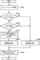
次に、図4のフローチャートを参照して、図3に示す設定処理によって設定された消去モードでデータの消去処理を行う具体的な手順について説明する。MFP1において動作しているOSのファイルシステム(FS)は、二次記憶装置6に格納されたファイルを管理している。図4に示す処理は、ファイルシステム上でファイル(データ)の削除が行われた際に実行される。なお、図4に示す各ステップの処理は、FPGAやASIC等のハードウェアにより実現されてもよいし、ソフトウェアにより実現されてもよい。ソフトウェアにより実現される場合、各処理は、CPU201が、二次記憶装置6等に格納された制御プログラムを読み出して実行する処理によって実現されてもよい。
第2実施形態では、二次記憶装置6としてSSDがMFP1に搭載された場合に、CPU201がSSDに対して、ファイルシステム上におけるデータの削除と同期してTrimコマンド(消去コマンド)を発行する例について説明する。以下では、説明の簡略化のため、第1実施形態と異なる点を中心として説明する。
以下では、図6のフローチャートを参照して、本実施形態に係る、二次記憶装置6に格納されたデータを消去する消去モードの設定処理の具体的な手順について説明する。図6に示す各ステップの処理は、図3と同様、FPGAやASIC等のハードウェアにより実現されてもよいし、ソフトウェアにより実現されてもよい。以下では、図3と異なる点を中心に説明する。
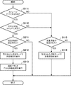
次に、図7のフローチャートを参照して、本実施形態に係る、図6に示す設定処理によって設定された消去モードでデータの消去処理を行う具体的な手順について説明する。図7に示す処理は、図4と同様、ファイルシステム上でファイル(データ)の削除が行われた際に実行される。また、図7に示す各ステップの処理は、図4と同様、FPGAやASIC等のハードウェアにより実現されてもよいし、ソフトウェアにより実現されてもよい。以下では、図4と異なる点を中心に説明する。
本発明は、上述の実施形態の1以上の機能を実現するプログラムを、ネットワーク又は記憶媒体を介してシステム又は装置に供給し、そのシステム又は装置のコンピュータにおける1つ以上のプロセッサーがプログラムを読出し実行する処理でも実現可能である。また、1以上の機能を実現する回路(例えば、ASIC)によっても実現可能である。
Claims (14)
- 情報処理装置であって、
前記情報処理装置が備えている記憶装置の装置情報を取得する取得手段と、
前記装置情報に基づいて、前記記憶装置が、当該記憶装置にデータの消去処理を実行させるための消去コマンドに対応する半導体記憶装置である場合には、前記消去コマンドによる消去処理を実行する少なくとも1つの消去モードのうち1つを選択可能な第1画面を表示させ、前記記憶装置が磁気記憶装置である場合には、前記消去コマンドを使用しない消去処理を実行する少なくとも1つの消去モードのうち1つを選択可能な第2画面を表示させる制御手段と、
を備えることを特徴とする情報処理装置。 - 前記制御手段は、前記記憶装置が前記消去コマンドに対応しない半導体記憶装置であれば、前記第1画面を表示させない
ことを特徴とする請求項1に記載の情報処理装置。 - 前記制御手段は、前記記憶装置が前記消去コマンドに対応しない半導体記憶装置であれば、前記第2画面を表示させる
ことを特徴とする請求項1又は2に記載の情報処理装置。 - 前記第1画面又は前記第2画面で選択された消去モードに基づいて、前記記憶装置に格納されたデータの消去を実行する実行手段を更に備える
ことを特徴とする請求項1から3のいずれか1項に記載の情報処理装置。 - 前記制御手段は、前記記憶装置が前記消去コマンドに対応する半導体記憶装置であれば、前記消去コマンドによる消去処理を行う消去モードと、前記消去コマンドを使用しない消去処理を行い、かつ、前記消去コマンドによる消去処理を行う消去モードとを選択可能に前記第1画面に表示させる
ことを特徴とする請求項1から4のいずれか1項に記載の情報処理装置。 - 前記実行手段は、前記記憶装置が前記消去コマンドに対応する半導体記憶装置であれば、前記消去コマンドを前記記憶装置に対して発行することで、当該消去コマンドによる消去処理を前記記憶装置に実行させる
ことを特徴とする請求項4に記載の情報処理装置。 - 前記実行手段は、前記記憶装置が前記消去コマンドに対応する半導体記憶装置であれば、前記情報処理装置のファイルシステム上で前記データの削除が行われたタイミングと非同期のタイミングに、前記消去コマンドを前記記憶装置に対して発行する
ことを特徴とする請求項6に記載の情報処理装置。 - 前記実行手段は、前記記憶装置が前記消去コマンドに対応する半導体記憶装置であれば、前記情報処理装置のファイルシステム上で前記データの削除が行われたタイミングと同期したタイミングに、前記消去コマンドを前記記憶装置に対して発行する
ことを特徴とする請求項6に記載の情報処理装置。 - 前記記憶装置が前記消去コマンドに対応する半導体記憶装置である場合に、
前記制御手段は、前記情報処理装置のファイルシステム上で前記データの削除が行われたタイミングと同期したタイミングに前記消去コマンドによる消去処理が行われることを示すメッセージを前記第1画面に表示させ、
前記実行手段は、前記第1画面において設定された消去モードによらず、前記情報処理装置のファイルシステム上で前記データの削除が行われたタイミングと同期したタイミングに、前記消去コマンドを前記記憶装置に対して発行する
ことを特徴とする請求項8に記載の情報処理装置。 - 前記消去モードは、ジョブの実行時に生成されたデータを当該ジョブの実行の完了後に前記記憶装置から消去するために設定される
ことを特徴とする請求項1から9のいずれか1項に記載の情報処理装置。 - 前記記憶装置に格納されるデータは、コピージョブの実行に用いられるデータを含むことを特徴とする請求項10に記載の情報処理装置。
- 前記消去モードは、前記コピージョブの実行に使用されたデータを前記ジョブの実行の完了後に前記記憶装置から消去するように設定される
ことを特徴とする請求項11に記載の情報処理装置。 - 前記消去コマンドに対応しないタイプの記憶装置はHDDであり、前記消去コマンドに対応するタイプの記憶装置はSSDである
ことを特徴とする請求項1から12のいずれか1項に記載の情報処理装置。 - 前記消去コマンドは、TRIMコマンドである
ことを特徴とする請求項1から13のいずれか1項に記載の情報処理装置。
Priority Applications (6)
| Application Number | Priority Date | Filing Date | Title |
|---|---|---|---|
| JP2016177141A JP6875808B2 (ja) | 2016-09-09 | 2016-09-09 | 情報処理装置 |
| EP17184410.3A EP3293626B1 (en) | 2016-09-09 | 2017-08-02 | Information processing apparatus and method of controlling the same |
| US15/684,190 US10452329B2 (en) | 2016-09-09 | 2017-08-23 | Information processing apparatus that controls display of an erasure mode setting screen based on a type of storage device in the apparatus, and method of controlling the same |
| KR1020170111564A KR102288563B1 (ko) | 2016-09-09 | 2017-09-01 | 정보 처리장치 및 그 제어방법 |
| CN201710798152.4A CN107807800B (zh) | 2016-09-09 | 2017-09-07 | 信息处理装置以及控制信息处理装置的方法 |
| CN202110940153.4A CN113641315B (zh) | 2016-09-09 | 2017-09-07 | 信息处理装置以及控制信息处理装置的方法 |
Applications Claiming Priority (1)
| Application Number | Priority Date | Filing Date | Title |
|---|---|---|---|
| JP2016177141A JP6875808B2 (ja) | 2016-09-09 | 2016-09-09 | 情報処理装置 |
Publications (3)
| Publication Number | Publication Date |
|---|---|
| JP2018041417A JP2018041417A (ja) | 2018-03-15 |
| JP2018041417A5 JP2018041417A5 (ja) | 2019-10-17 |
| JP6875808B2 true JP6875808B2 (ja) | 2021-05-26 |
Family
ID=59564094
Family Applications (1)
| Application Number | Title | Priority Date | Filing Date |
|---|---|---|---|
| JP2016177141A Active JP6875808B2 (ja) | 2016-09-09 | 2016-09-09 | 情報処理装置 |
Country Status (5)
| Country | Link |
|---|---|
| US (1) | US10452329B2 (ja) |
| EP (1) | EP3293626B1 (ja) |
| JP (1) | JP6875808B2 (ja) |
| KR (1) | KR102288563B1 (ja) |
| CN (2) | CN107807800B (ja) |
Families Citing this family (6)
| Publication number | Priority date | Publication date | Assignee | Title |
|---|---|---|---|---|
| JP6892361B2 (ja) | 2017-09-21 | 2021-06-23 | キオクシア株式会社 | ストレージ装置 |
| CN110568998B (zh) * | 2019-09-16 | 2023-06-06 | 深圳忆联信息系统有限公司 | 基于固态硬盘的Trim命令实现方法、装置和计算机设备 |
| JP7467088B2 (ja) * | 2019-12-03 | 2024-04-15 | キヤノン株式会社 | 情報処理装置、情報処理装置の処理方法およびプログラム |
| JP2021100182A (ja) * | 2019-12-20 | 2021-07-01 | キヤノン株式会社 | 画像形成装置および画像形成装置の制御方法 |
| JP2021099642A (ja) * | 2019-12-20 | 2021-07-01 | キヤノン株式会社 | 情報処理装置および情報処理装置の制御方法 |
| JP2021175018A (ja) * | 2020-04-20 | 2021-11-01 | コニカミノルタ株式会社 | 画像形成装置 |
Family Cites Families (27)
| Publication number | Priority date | Publication date | Assignee | Title |
|---|---|---|---|---|
| US6731447B2 (en) * | 2001-06-04 | 2004-05-04 | Xerox Corporation | Secure data file erasure |
| JP4387687B2 (ja) * | 2002-04-26 | 2009-12-16 | キヤノン株式会社 | 画像処理装置、制御方法、及びプログラム |
| EP3174277B1 (en) * | 2003-02-25 | 2018-10-31 | SHARP Kabushiki Kaisha | Image processing apparatus |
| JP2005018415A (ja) * | 2003-06-26 | 2005-01-20 | Toshiba Corp | 情報処理装置および同装置で使用されるデータ消去方法 |
| JP4140897B2 (ja) * | 2003-08-08 | 2008-08-27 | 株式会社リコー | 記憶装置および画像形成装置 |
| JP2005244656A (ja) * | 2004-02-26 | 2005-09-08 | Matsushita Electric Ind Co Ltd | 複合機 |
| JP2006023854A (ja) * | 2004-07-06 | 2006-01-26 | Sharp Corp | 情報処理装置、記憶装置、記憶制御装置及びプログラム |
| JP4976759B2 (ja) * | 2006-06-29 | 2012-07-18 | 株式会社沖データ | 画像処理装置 |
| JP5404097B2 (ja) * | 2009-02-27 | 2014-01-29 | キヤノン株式会社 | 画像処理装置、その制御方法、及びプログラム |
| US8433843B2 (en) * | 2009-03-31 | 2013-04-30 | Qualcomm Incorporated | Method for protecting sensitive data on a storage device having wear leveling |
| JP5523040B2 (ja) * | 2009-09-29 | 2014-06-18 | キヤノン株式会社 | 画像処理装置、制御方法、及びプログラム |
| KR20120130763A (ko) * | 2010-02-05 | 2012-12-03 | 가부시키가이샤 한도오따이 에네루기 켄큐쇼 | 반도체 장치 및 반도체 장치의 제조 방법 |
| JP5488049B2 (ja) * | 2010-02-26 | 2014-05-14 | 富士通株式会社 | 情報処理装置及び実行方法 |
| JP5538970B2 (ja) * | 2010-03-25 | 2014-07-02 | キヤノン株式会社 | 情報処理装置、データ処理方法、プログラム |
| JP5574858B2 (ja) * | 2010-07-07 | 2014-08-20 | キヤノン株式会社 | 情報処理装置、情報処理装置の制御方法、プログラム |
| US8452911B2 (en) * | 2010-09-30 | 2013-05-28 | Sandisk Technologies Inc. | Synchronized maintenance operations in a multi-bank storage system |
| CN102157390B (zh) * | 2011-01-25 | 2013-03-27 | 日月光半导体(昆山)有限公司 | 自动去除半导体封装不良品的机台及方法 |
| JP5786611B2 (ja) * | 2011-09-30 | 2015-09-30 | 富士通株式会社 | ストレージ装置およびストレージシステム |
| JP5586718B2 (ja) * | 2012-06-19 | 2014-09-10 | 株式会社東芝 | 制御プログラム、ホスト装置の制御方法、情報処理装置およびホスト装置 |
| DE102012022728A1 (de) * | 2012-11-21 | 2014-05-22 | Unify Gmbh & Co. Kg | Verfahren zur Steuerung eines Flash-Speichers zur Massenspeicherung, der von einem an einen Host anschließbaren Kommunikationsgerät umfasst ist, und Computerprogrammprodukt zur Ausführung des Verfahrens |
| JP5746234B2 (ja) * | 2013-01-30 | 2015-07-08 | 株式会社東芝 | 画像形成装置、消去装置 |
| JP6271939B2 (ja) * | 2013-10-11 | 2018-01-31 | キヤノン株式会社 | 情報処理装置及びその制御方法、並びにプログラム |
| JP6489751B2 (ja) | 2014-03-27 | 2019-03-27 | キヤノン株式会社 | データ処理装置とその制御方法、及びプログラム |
| JP2015204071A (ja) * | 2014-04-16 | 2015-11-16 | キヤノン株式会社 | 情報処理装置、情報処理方法およびプログラム |
| CN106716333B (zh) * | 2014-04-23 | 2020-01-17 | 数据隐藏技术有限责任公司 | 用于完成安全擦除操作的方法 |
| JP6525507B2 (ja) * | 2014-05-14 | 2019-06-05 | キヤノン株式会社 | 情報処理装置、情報処理方法及びプログラム |
| CN105513640B (zh) * | 2015-12-03 | 2020-04-14 | 深圳佰维存储科技股份有限公司 | 一种固态硬盘数据擦除方法及其系统 |
-
2016
- 2016-09-09 JP JP2016177141A patent/JP6875808B2/ja active Active
-
2017
- 2017-08-02 EP EP17184410.3A patent/EP3293626B1/en active Active
- 2017-08-23 US US15/684,190 patent/US10452329B2/en active Active
- 2017-09-01 KR KR1020170111564A patent/KR102288563B1/ko active Active
- 2017-09-07 CN CN201710798152.4A patent/CN107807800B/zh active Active
- 2017-09-07 CN CN202110940153.4A patent/CN113641315B/zh active Active
Also Published As
| Publication number | Publication date |
|---|---|
| US10452329B2 (en) | 2019-10-22 |
| CN113641315B (zh) | 2024-08-09 |
| EP3293626A1 (en) | 2018-03-14 |
| CN107807800B (zh) | 2021-08-24 |
| CN113641315A (zh) | 2021-11-12 |
| KR102288563B1 (ko) | 2021-08-11 |
| US20180074766A1 (en) | 2018-03-15 |
| JP2018041417A (ja) | 2018-03-15 |
| CN107807800A (zh) | 2018-03-16 |
| EP3293626B1 (en) | 2022-10-12 |
| KR20180028925A (ko) | 2018-03-19 |
Similar Documents
| Publication | Publication Date | Title |
|---|---|---|
| JP6875808B2 (ja) | 情報処理装置 | |
| JP5630984B2 (ja) | 画像入出力装置及び画像入出力方法 | |
| JP5213539B2 (ja) | 画像処理装置及び画像処理装置のメモリ管理方法 | |
| JP5506568B2 (ja) | データ処理装置、データ処理装置のデータ処理方法、プログラム | |
| JP2015219602A (ja) | 情報処理装置、情報処理方法及びプログラム | |
| JP2008070975A (ja) | データ保存装置及びデータ保存方法 | |
| JP2015141603A (ja) | 画像処理装置およびその制御方法、並びにプログラム | |
| JP2016206938A (ja) | 情報処理システム、情報処理システムのメモリ制御方法、及びプログラム | |
| JP2018063676A (ja) | 情報処理装置及びその制御方法、並びにプログラム | |
| JP4218582B2 (ja) | 画像形成装置 | |
| JP4479324B2 (ja) | 情報処理装置 | |
| JP6995607B2 (ja) | 情報処理装置、情報処理装置の制御方法及びプログラム | |
| CN107797762B (zh) | 信息处理装置及信息处理方法 | |
| JP7238087B2 (ja) | ジョブ処理装置、ジョブ処理装置の制御方法及びプログラム | |
| JP2015204071A (ja) | 情報処理装置、情報処理方法およびプログラム | |
| JP5544905B2 (ja) | 画像処理装置と画像処理装置のデータ消去方法とプログラム | |
| CN108307087B (zh) | 信息处理装置及计算机能够读取的存储介质 | |
| JP6395380B2 (ja) | 情報処理装置、情報処理方法、及びプログラム | |
| JP2006195517A (ja) | 画像処理装置、画像処理プログラム、画像処理方法 | |
| JP2021179731A (ja) | 情報処理装置、情報処理装置の制御方法、及びプログラム | |
| JP2011160247A6 (ja) | 画像処理装置と画像処理装置のデータ消去方法とプログラム | |
| JP2006276908A (ja) | 情報処理装置、情報処理方法、及びプログラム | |
| JP2021072016A (ja) | 画像形成装置、その制御方法、及びプログラム | |
| JP2010079736A (ja) | 情報処理装置、画像形成装置、及びプログラム | |
| JP2020109591A (ja) | 情報処理装置、その制御方法およびプログラム |
Legal Events
| Date | Code | Title | Description |
|---|---|---|---|
| A521 | Request for written amendment filed |
Free format text: JAPANESE INTERMEDIATE CODE: A523 Effective date: 20190904 |
|
| A621 | Written request for application examination |
Free format text: JAPANESE INTERMEDIATE CODE: A621 Effective date: 20190904 |
|
| A977 | Report on retrieval |
Free format text: JAPANESE INTERMEDIATE CODE: A971007 Effective date: 20200722 |
|
| A131 | Notification of reasons for refusal |
Free format text: JAPANESE INTERMEDIATE CODE: A131 Effective date: 20200814 |
|
| A521 | Request for written amendment filed |
Free format text: JAPANESE INTERMEDIATE CODE: A523 Effective date: 20201013 |
|
| RD01 | Notification of change of attorney |
Free format text: JAPANESE INTERMEDIATE CODE: A7421 Effective date: 20210103 |
|
| A521 | Request for written amendment filed |
Free format text: JAPANESE INTERMEDIATE CODE: A523 Effective date: 20210113 |
|
| TRDD | Decision of grant or rejection written | ||
| A01 | Written decision to grant a patent or to grant a registration (utility model) |
Free format text: JAPANESE INTERMEDIATE CODE: A01 Effective date: 20210326 |
|
| A61 | First payment of annual fees (during grant procedure) |
Free format text: JAPANESE INTERMEDIATE CODE: A61 Effective date: 20210423 |
|
| R151 | Written notification of patent or utility model registration |
Ref document number: 6875808 Country of ref document: JP Free format text: JAPANESE INTERMEDIATE CODE: R151 |