JP6877290B2 - 被処理体を処理する方法 - Google Patents
被処理体を処理する方法 Download PDFInfo
- Publication number
- JP6877290B2 JP6877290B2 JP2017150927A JP2017150927A JP6877290B2 JP 6877290 B2 JP6877290 B2 JP 6877290B2 JP 2017150927 A JP2017150927 A JP 2017150927A JP 2017150927 A JP2017150927 A JP 2017150927A JP 6877290 B2 JP6877290 B2 JP 6877290B2
- Authority
- JP
- Japan
- Prior art keywords
- film
- gas
- via hole
- insulating film
- trench
- Prior art date
- Legal status (The legal status is an assumption and is not a legal conclusion. Google has not performed a legal analysis and makes no representation as to the accuracy of the status listed.)
- Active
Links
Images




Classifications
-
- H—ELECTRICITY
- H10—SEMICONDUCTOR DEVICES; ELECTRIC SOLID-STATE DEVICES NOT OTHERWISE PROVIDED FOR
- H10W—GENERIC PACKAGES, INTERCONNECTIONS, CONNECTORS OR OTHER CONSTRUCTIONAL DETAILS OF DEVICES COVERED BY CLASS H10
- H10W20/00—Interconnections in chips, wafers or substrates
- H10W20/01—Manufacture or treatment
- H10W20/071—Manufacture or treatment of dielectric parts thereof
- H10W20/081—Manufacture or treatment of dielectric parts thereof by forming openings in the dielectric parts
- H10W20/084—Manufacture or treatment of dielectric parts thereof by forming openings in the dielectric parts for dual-damascene structures
-
- H—ELECTRICITY
- H10—SEMICONDUCTOR DEVICES; ELECTRIC SOLID-STATE DEVICES NOT OTHERWISE PROVIDED FOR
- H10W—GENERIC PACKAGES, INTERCONNECTIONS, CONNECTORS OR OTHER CONSTRUCTIONAL DETAILS OF DEVICES COVERED BY CLASS H10
- H10W20/00—Interconnections in chips, wafers or substrates
- H10W20/01—Manufacture or treatment
- H10W20/031—Manufacture or treatment of conductive parts of the interconnections
- H10W20/032—Manufacture or treatment of conductive parts of the interconnections of conductive barrier, adhesion or liner layers
- H10W20/054—Manufacture or treatment of conductive parts of the interconnections of conductive barrier, adhesion or liner layers by selectively removing parts thereof
-
- H—ELECTRICITY
- H10—SEMICONDUCTOR DEVICES; ELECTRIC SOLID-STATE DEVICES NOT OTHERWISE PROVIDED FOR
- H10P—GENERIC PROCESSES OR APPARATUS FOR THE MANUFACTURE OR TREATMENT OF DEVICES COVERED BY CLASS H10
- H10P14/00—Formation of materials, e.g. in the shape of layers or pillars
- H10P14/60—Formation of materials, e.g. in the shape of layers or pillars of insulating materials
- H10P14/63—Formation of materials, e.g. in the shape of layers or pillars of insulating materials characterised by the formation processes
- H10P14/6326—Deposition processes
- H10P14/6328—Deposition from the gas or vapour phase
- H10P14/6334—Deposition from the gas or vapour phase using decomposition or reaction of gaseous or vapour phase compounds, i.e. chemical vapour deposition
- H10P14/6339—Deposition from the gas or vapour phase using decomposition or reaction of gaseous or vapour phase compounds, i.e. chemical vapour deposition deposition by cyclic CVD, e.g. ALD, ALE or pulsed CVD
-
- H—ELECTRICITY
- H10—SEMICONDUCTOR DEVICES; ELECTRIC SOLID-STATE DEVICES NOT OTHERWISE PROVIDED FOR
- H10P—GENERIC PROCESSES OR APPARATUS FOR THE MANUFACTURE OR TREATMENT OF DEVICES COVERED BY CLASS H10
- H10P14/00—Formation of materials, e.g. in the shape of layers or pillars
- H10P14/60—Formation of materials, e.g. in the shape of layers or pillars of insulating materials
- H10P14/69—Inorganic materials
- H10P14/692—Inorganic materials composed of oxides, glassy oxides or oxide-based glasses
- H10P14/6921—Inorganic materials composed of oxides, glassy oxides or oxide-based glasses containing silicon
- H10P14/69215—Inorganic materials composed of oxides, glassy oxides or oxide-based glasses containing silicon the material being a silicon oxide, e.g. SiO2
-
- H—ELECTRICITY
- H10—SEMICONDUCTOR DEVICES; ELECTRIC SOLID-STATE DEVICES NOT OTHERWISE PROVIDED FOR
- H10P—GENERIC PROCESSES OR APPARATUS FOR THE MANUFACTURE OR TREATMENT OF DEVICES COVERED BY CLASS H10
- H10P50/00—Etching of wafers, substrates or parts of devices
- H10P50/20—Dry etching; Plasma etching; Reactive-ion etching
- H10P50/28—Dry etching; Plasma etching; Reactive-ion etching of insulating materials
- H10P50/282—Dry etching; Plasma etching; Reactive-ion etching of insulating materials of inorganic materials
- H10P50/283—Dry etching; Plasma etching; Reactive-ion etching of insulating materials of inorganic materials by chemical means
-
- H—ELECTRICITY
- H10—SEMICONDUCTOR DEVICES; ELECTRIC SOLID-STATE DEVICES NOT OTHERWISE PROVIDED FOR
- H10P—GENERIC PROCESSES OR APPARATUS FOR THE MANUFACTURE OR TREATMENT OF DEVICES COVERED BY CLASS H10
- H10P50/00—Etching of wafers, substrates or parts of devices
- H10P50/20—Dry etching; Plasma etching; Reactive-ion etching
- H10P50/28—Dry etching; Plasma etching; Reactive-ion etching of insulating materials
- H10P50/286—Dry etching; Plasma etching; Reactive-ion etching of insulating materials of organic materials
- H10P50/287—Dry etching; Plasma etching; Reactive-ion etching of insulating materials of organic materials by chemical means
-
- H—ELECTRICITY
- H10—SEMICONDUCTOR DEVICES; ELECTRIC SOLID-STATE DEVICES NOT OTHERWISE PROVIDED FOR
- H10P—GENERIC PROCESSES OR APPARATUS FOR THE MANUFACTURE OR TREATMENT OF DEVICES COVERED BY CLASS H10
- H10P50/00—Etching of wafers, substrates or parts of devices
- H10P50/73—Etching of wafers, substrates or parts of devices using masks for insulating materials
-
- H—ELECTRICITY
- H10—SEMICONDUCTOR DEVICES; ELECTRIC SOLID-STATE DEVICES NOT OTHERWISE PROVIDED FOR
- H10P—GENERIC PROCESSES OR APPARATUS FOR THE MANUFACTURE OR TREATMENT OF DEVICES COVERED BY CLASS H10
- H10P76/00—Manufacture or treatment of masks on semiconductor bodies, e.g. by lithography or photolithography
- H10P76/20—Manufacture or treatment of masks on semiconductor bodies, e.g. by lithography or photolithography of masks comprising organic materials
- H10P76/204—Manufacture or treatment of masks on semiconductor bodies, e.g. by lithography or photolithography of masks comprising organic materials of organic photoresist masks
- H10P76/2041—Photolithographic processes
-
- H—ELECTRICITY
- H10—SEMICONDUCTOR DEVICES; ELECTRIC SOLID-STATE DEVICES NOT OTHERWISE PROVIDED FOR
- H10P—GENERIC PROCESSES OR APPARATUS FOR THE MANUFACTURE OR TREATMENT OF DEVICES COVERED BY CLASS H10
- H10P76/00—Manufacture or treatment of masks on semiconductor bodies, e.g. by lithography or photolithography
- H10P76/40—Manufacture or treatment of masks on semiconductor bodies, e.g. by lithography or photolithography of masks comprising inorganic materials
- H10P76/408—Manufacture or treatment of masks on semiconductor bodies, e.g. by lithography or photolithography of masks comprising inorganic materials characterised by their sizes, orientations, dispositions, behaviours or shapes
- H10P76/4085—Manufacture or treatment of masks on semiconductor bodies, e.g. by lithography or photolithography of masks comprising inorganic materials characterised by their sizes, orientations, dispositions, behaviours or shapes characterised by the processes involved to create the masks
-
- H—ELECTRICITY
- H10—SEMICONDUCTOR DEVICES; ELECTRIC SOLID-STATE DEVICES NOT OTHERWISE PROVIDED FOR
- H10W—GENERIC PACKAGES, INTERCONNECTIONS, CONNECTORS OR OTHER CONSTRUCTIONAL DETAILS OF DEVICES COVERED BY CLASS H10
- H10W20/00—Interconnections in chips, wafers or substrates
- H10W20/01—Manufacture or treatment
- H10W20/031—Manufacture or treatment of conductive parts of the interconnections
- H10W20/032—Manufacture or treatment of conductive parts of the interconnections of conductive barrier, adhesion or liner layers
- H10W20/033—Manufacture or treatment of conductive parts of the interconnections of conductive barrier, adhesion or liner layers in openings in dielectrics
-
- H—ELECTRICITY
- H10—SEMICONDUCTOR DEVICES; ELECTRIC SOLID-STATE DEVICES NOT OTHERWISE PROVIDED FOR
- H10W—GENERIC PACKAGES, INTERCONNECTIONS, CONNECTORS OR OTHER CONSTRUCTIONAL DETAILS OF DEVICES COVERED BY CLASS H10
- H10W20/00—Interconnections in chips, wafers or substrates
- H10W20/01—Manufacture or treatment
- H10W20/071—Manufacture or treatment of dielectric parts thereof
- H10W20/074—Manufacture or treatment of dielectric parts thereof of dielectric parts comprising thin functional dielectric layers, e.g. dielectric etch-stop, barrier, capping or liner layers
-
- H—ELECTRICITY
- H10—SEMICONDUCTOR DEVICES; ELECTRIC SOLID-STATE DEVICES NOT OTHERWISE PROVIDED FOR
- H10W—GENERIC PACKAGES, INTERCONNECTIONS, CONNECTORS OR OTHER CONSTRUCTIONAL DETAILS OF DEVICES COVERED BY CLASS H10
- H10W20/00—Interconnections in chips, wafers or substrates
- H10W20/01—Manufacture or treatment
- H10W20/071—Manufacture or treatment of dielectric parts thereof
- H10W20/074—Manufacture or treatment of dielectric parts thereof of dielectric parts comprising thin functional dielectric layers, e.g. dielectric etch-stop, barrier, capping or liner layers
- H10W20/076—Manufacture or treatment of dielectric parts thereof of dielectric parts comprising thin functional dielectric layers, e.g. dielectric etch-stop, barrier, capping or liner layers in via holes or trenches
-
- H—ELECTRICITY
- H10—SEMICONDUCTOR DEVICES; ELECTRIC SOLID-STATE DEVICES NOT OTHERWISE PROVIDED FOR
- H10W—GENERIC PACKAGES, INTERCONNECTIONS, CONNECTORS OR OTHER CONSTRUCTIONAL DETAILS OF DEVICES COVERED BY CLASS H10
- H10W20/00—Interconnections in chips, wafers or substrates
- H10W20/01—Manufacture or treatment
- H10W20/071—Manufacture or treatment of dielectric parts thereof
- H10W20/081—Manufacture or treatment of dielectric parts thereof by forming openings in the dielectric parts
- H10W20/083—Manufacture or treatment of dielectric parts thereof by forming openings in the dielectric parts the openings being via holes penetrating underlying conductors
-
- H—ELECTRICITY
- H10—SEMICONDUCTOR DEVICES; ELECTRIC SOLID-STATE DEVICES NOT OTHERWISE PROVIDED FOR
- H10W—GENERIC PACKAGES, INTERCONNECTIONS, CONNECTORS OR OTHER CONSTRUCTIONAL DETAILS OF DEVICES COVERED BY CLASS H10
- H10W20/00—Interconnections in chips, wafers or substrates
- H10W20/01—Manufacture or treatment
- H10W20/071—Manufacture or treatment of dielectric parts thereof
- H10W20/081—Manufacture or treatment of dielectric parts thereof by forming openings in the dielectric parts
- H10W20/084—Manufacture or treatment of dielectric parts thereof by forming openings in the dielectric parts for dual-damascene structures
- H10W20/087—Manufacture or treatment of dielectric parts thereof by forming openings in the dielectric parts for dual-damascene structures involving multiple stacked pre-patterned masks
-
- H—ELECTRICITY
- H10—SEMICONDUCTOR DEVICES; ELECTRIC SOLID-STATE DEVICES NOT OTHERWISE PROVIDED FOR
- H10W—GENERIC PACKAGES, INTERCONNECTIONS, CONNECTORS OR OTHER CONSTRUCTIONAL DETAILS OF DEVICES COVERED BY CLASS H10
- H10W20/00—Interconnections in chips, wafers or substrates
- H10W20/01—Manufacture or treatment
- H10W20/071—Manufacture or treatment of dielectric parts thereof
- H10W20/081—Manufacture or treatment of dielectric parts thereof by forming openings in the dielectric parts
- H10W20/084—Manufacture or treatment of dielectric parts thereof by forming openings in the dielectric parts for dual-damascene structures
- H10W20/088—Manufacture or treatment of dielectric parts thereof by forming openings in the dielectric parts for dual-damascene structures involving partial etching of via holes
-
- H—ELECTRICITY
- H10—SEMICONDUCTOR DEVICES; ELECTRIC SOLID-STATE DEVICES NOT OTHERWISE PROVIDED FOR
- H10W—GENERIC PACKAGES, INTERCONNECTIONS, CONNECTORS OR OTHER CONSTRUCTIONAL DETAILS OF DEVICES COVERED BY CLASS H10
- H10W20/00—Interconnections in chips, wafers or substrates
- H10W20/01—Manufacture or treatment
- H10W20/071—Manufacture or treatment of dielectric parts thereof
- H10W20/093—Manufacture or treatment of dielectric parts thereof by modifying materials of the dielectric parts
- H10W20/096—Manufacture or treatment of dielectric parts thereof by modifying materials of the dielectric parts by contacting with gases, liquids or plasmas
-
- H—ELECTRICITY
- H10—SEMICONDUCTOR DEVICES; ELECTRIC SOLID-STATE DEVICES NOT OTHERWISE PROVIDED FOR
- H10W—GENERIC PACKAGES, INTERCONNECTIONS, CONNECTORS OR OTHER CONSTRUCTIONAL DETAILS OF DEVICES COVERED BY CLASS H10
- H10W20/00—Interconnections in chips, wafers or substrates
- H10W20/01—Manufacture or treatment
- H10W20/071—Manufacture or treatment of dielectric parts thereof
- H10W20/074—Manufacture or treatment of dielectric parts thereof of dielectric parts comprising thin functional dielectric layers, e.g. dielectric etch-stop, barrier, capping or liner layers
- H10W20/076—Manufacture or treatment of dielectric parts thereof of dielectric parts comprising thin functional dielectric layers, e.g. dielectric etch-stop, barrier, capping or liner layers in via holes or trenches
- H10W20/0765—Manufacture or treatment of dielectric parts thereof of dielectric parts comprising thin functional dielectric layers, e.g. dielectric etch-stop, barrier, capping or liner layers in via holes or trenches the thin functional dielectric layers being temporary, e.g. sacrificial layers
Landscapes
- Internal Circuitry In Semiconductor Integrated Circuit Devices (AREA)
- Drying Of Semiconductors (AREA)
- Physics & Mathematics (AREA)
- Engineering & Computer Science (AREA)
- Plasma & Fusion (AREA)
- Formation Of Insulating Films (AREA)
- Separation By Low-Temperature Treatments (AREA)
- Heating, Cooling, Or Curing Plastics Or The Like In General (AREA)
- Physical Or Chemical Processes And Apparatus (AREA)
Description
条件(i):工程ST1ebにおける犠牲膜EXおよび第2の絶縁膜IS2に対するエッチングの実行時間は、ビア孔VH1の深さ(ビア孔VH1の底面BFからビア孔VH1の開口までのビア孔VH1の側面SFの長さ)を犠牲膜EXのエッチングレートで割って得られる商の値以上である。
条件(ii):犠牲膜EXのエッチングレートと第2の絶縁膜IS2のエッチングレートとは同程度である。
Claims (12)
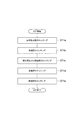
- 被処理体を処理する方法であって、該被処理体は、配線を有する配線層、該配線層上に設けられた拡散防止膜、該拡散防止膜上に設けられた絶縁膜、該絶縁膜上に設けられ開口を提供する金属マスクを備え、該絶縁膜は、該開口から露出される箇所の一部に設けられたトレンチ、および該トレンチの一部に設けられた第1のビア孔を備え、該方法は、
前記被処理体の前記トレンチと前記第1のビア孔の側面とに犠牲膜を形成する第1の工程と、
前記犠牲膜および前記絶縁膜に対しエッチングを行って、前記第1のビア孔の底面の更に深い位置に第2のビア孔を形成し、該トレンチおよび該第1のビア孔から該犠牲膜を除去する第2の工程と、
を備える方法。 - 第2の工程が完了したとき、前記トレンチの深さは更に深くなり、且つ、前記第1のビア孔はエッチングによって消滅している、
請求項1に記載の方法。 - 前記第1の工程において、前記犠牲膜はコンフォーマルに形成される、
請求項1または請求項2に記載の方法。 - 前記第1の工程は、
ALD(Atomic Layer Deposition)方式を用いて前記トレンチの側面を含む前記被処理体の表面に前記犠牲膜を形成する第3の工程と、
前記被処理体の表面に形成された前記犠牲膜に対しエッチングを行って、前記トレンチの底面を露出させる第4の工程と、
を備える、
請求項1〜3の何れか一項に記載の方法。 - 前記絶縁膜は、シリコン酸化膜、低誘電率の特性を有するシリコン含有膜、または、シリコン酸化膜と低誘電率の特性を有するシリコン含有膜とが積層される膜である、
請求項1〜4の何れか一項に記載の方法。 - 前記犠牲膜は、低誘電率の特性を有する、
請求項1〜5の何れか一項に記載の方法。 - 前記犠牲膜は、シリコン酸化膜である、
請求項1〜6の何れか一項に記載の方法。 - 前記第1の工程から前記第2の工程までは、真空一貫の環境において実行される、
請求項1〜7の何れか一項に記載の方法。 - 前記第1の工程から前記第2の工程までは、単一の処理容器内で実行される、
請求項1〜8の何れか一項に記載の方法。 - 前記絶縁膜の材料が細孔を有する多孔質材である場合に、前記第1の工程は、前記犠牲膜を形成する前に、前記トレンチの表面に露出される該多孔質材の表層に位置する該細孔を封孔する処理を行う、
請求項1〜9の何れか一項に記載の方法。 - 前記ビア孔が前記拡散防止膜に至るまで、前記第1の工程と前記第2の工程とを含むシーケンスを繰り返し実行する、
請求項1〜10の何れか一項に記載の方法。 - 前記第2の工程において行われる前記犠牲膜および前記絶縁膜に対するエッチングの実行時間は前記トレンチの深さを該犠牲膜のエッチングレートで割って得られる商の値以上であり、該犠牲膜のエッチングレートと該絶縁膜のエッチングレートとは同程度である、
請求項1〜11の何れか一項に記載の方法。
Priority Applications (5)
| Application Number | Priority Date | Filing Date | Title |
|---|---|---|---|
| JP2017150927A JP6877290B2 (ja) | 2017-08-03 | 2017-08-03 | 被処理体を処理する方法 |
| TW107125297A TWI780185B (zh) | 2017-08-03 | 2018-07-23 | 處理被處理體之方法 |
| US16/050,525 US10998223B2 (en) | 2017-08-03 | 2018-07-31 | Method for processing target object |
| KR1020180089802A KR102678853B1 (ko) | 2017-08-03 | 2018-08-01 | 피처리체를 처리하는 방법 |
| CN201810877048.9A CN109390274B (zh) | 2017-08-03 | 2018-08-03 | 对被处理体进行处理的方法 |
Applications Claiming Priority (1)
| Application Number | Priority Date | Filing Date | Title |
|---|---|---|---|
| JP2017150927A JP6877290B2 (ja) | 2017-08-03 | 2017-08-03 | 被処理体を処理する方法 |
Publications (2)
| Publication Number | Publication Date |
|---|---|
| JP2019029619A JP2019029619A (ja) | 2019-02-21 |
| JP6877290B2 true JP6877290B2 (ja) | 2021-05-26 |
Family
ID=65229953
Family Applications (1)
| Application Number | Title | Priority Date | Filing Date |
|---|---|---|---|
| JP2017150927A Active JP6877290B2 (ja) | 2017-08-03 | 2017-08-03 | 被処理体を処理する方法 |
Country Status (5)
| Country | Link |
|---|---|
| US (1) | US10998223B2 (ja) |
| JP (1) | JP6877290B2 (ja) |
| KR (1) | KR102678853B1 (ja) |
| CN (1) | CN109390274B (ja) |
| TW (1) | TWI780185B (ja) |
Families Citing this family (3)
| Publication number | Priority date | Publication date | Assignee | Title |
|---|---|---|---|---|
| US10204829B1 (en) * | 2018-01-12 | 2019-02-12 | International Business Machines Corporation | Low-resistivity metallic interconnect structures with self-forming diffusion barrier layers |
| CN109860432B (zh) * | 2018-12-17 | 2021-01-15 | 深圳市华星光电技术有限公司 | 显示器封装结构及其制造方法 |
| US11631589B2 (en) * | 2021-05-04 | 2023-04-18 | Applied Materials, Inc. | Metal etch in high aspect-ratio features |
Family Cites Families (27)
| Publication number | Priority date | Publication date | Assignee | Title |
|---|---|---|---|---|
| TW411503B (en) * | 1999-07-23 | 2000-11-11 | Taiwan Semiconductor Mfg | Method of forming bottom anti-reflective coating on substrate |
| JP2001358218A (ja) * | 2000-04-13 | 2001-12-26 | Canon Inc | 有機膜のエッチング方法及び素子の製造方法 |
| JP4477750B2 (ja) * | 2000-06-26 | 2010-06-09 | 東京エレクトロン株式会社 | エッチング方法 |
| JP2002373937A (ja) * | 2001-06-15 | 2002-12-26 | Fujitsu Ltd | 半導体装置及びその製造方法 |
| JP3962339B2 (ja) * | 2002-03-27 | 2007-08-22 | 松下電器産業株式会社 | 電子デバイスの製造方法 |
| DE10228807B4 (de) * | 2002-06-27 | 2009-07-23 | Advanced Micro Devices, Inc., Sunnyvale | Verfahren zur Herstellung von Mikrostrukturelementen |
| US7701060B2 (en) * | 2003-05-29 | 2010-04-20 | Nec Corporation | Wiring structure and method for manufacturing the same |
| JP4057972B2 (ja) * | 2003-07-25 | 2008-03-05 | 富士通株式会社 | 半導体装置の製造方法 |
| KR100632473B1 (ko) * | 2004-08-03 | 2006-10-09 | 삼성전자주식회사 | 염기성 물질 확산 장벽막을 사용하는 미세 전자 소자의듀얼 다마신 배선의 제조 방법 |
| JP2006156486A (ja) * | 2004-11-25 | 2006-06-15 | Tokyo Electron Ltd | 基板処理方法および半導体装置の製造方法 |
| US7309653B2 (en) * | 2005-02-24 | 2007-12-18 | International Business Machines Corporation | Method of forming damascene filament wires and the structure so formed |
| US7491647B2 (en) * | 2005-03-08 | 2009-02-17 | Lam Research Corporation | Etch with striation control |
| JP4197691B2 (ja) * | 2005-06-21 | 2008-12-17 | 株式会社東芝 | 半導体装置の製造方法 |
| JP2007123766A (ja) | 2005-10-31 | 2007-05-17 | Tokyo Electron Ltd | エッチング方法、プラズマ処理装置及び記憶媒体 |
| CN101667555B (zh) * | 2005-12-07 | 2012-06-27 | 佳能株式会社 | 使用双镶嵌工艺制造半导体器件的方法以及制造具有连通孔的制品的方法 |
| JP4666308B2 (ja) * | 2006-02-24 | 2011-04-06 | 富士通セミコンダクター株式会社 | 半導体装置の製造方法 |
| CN100517606C (zh) * | 2006-12-22 | 2009-07-22 | 中芯国际集成电路制造(上海)有限公司 | 通孔刻蚀方法 |
| US7767578B2 (en) * | 2007-01-11 | 2010-08-03 | United Microelectronics Corp. | Damascene interconnection structure and dual damascene process thereof |
| US7741218B2 (en) * | 2007-02-27 | 2010-06-22 | Freescale Semiconductor, Inc. | Conductive via formation utilizing electroplating |
| JP5342811B2 (ja) * | 2008-06-09 | 2013-11-13 | 東京エレクトロン株式会社 | 半導体装置の製造方法 |
| US8236684B2 (en) * | 2008-06-27 | 2012-08-07 | Applied Materials, Inc. | Prevention and reduction of solvent and solution penetration into porous dielectrics using a thin barrier layer |
| JP5391594B2 (ja) * | 2008-07-02 | 2014-01-15 | 富士通セミコンダクター株式会社 | 半導体装置の製造方法 |
| US8435901B2 (en) * | 2010-06-11 | 2013-05-07 | Tokyo Electron Limited | Method of selectively etching an insulation stack for a metal interconnect |
| US9184054B1 (en) * | 2014-04-25 | 2015-11-10 | Taiwan Semiconductor Manufacturing Company, Ltd. | Method for integrated circuit patterning |
| JP6373150B2 (ja) | 2014-06-16 | 2018-08-15 | 東京エレクトロン株式会社 | 基板処理システム及び基板処理方法 |
| JP2017059750A (ja) * | 2015-09-18 | 2017-03-23 | 東京エレクトロン株式会社 | 被処理体を処理する方法 |
| JP6537473B2 (ja) * | 2015-10-06 | 2019-07-03 | 東京エレクトロン株式会社 | 被処理体を処理する方法 |
-
2017
- 2017-08-03 JP JP2017150927A patent/JP6877290B2/ja active Active
-
2018
- 2018-07-23 TW TW107125297A patent/TWI780185B/zh active
- 2018-07-31 US US16/050,525 patent/US10998223B2/en active Active
- 2018-08-01 KR KR1020180089802A patent/KR102678853B1/ko active Active
- 2018-08-03 CN CN201810877048.9A patent/CN109390274B/zh active Active
Also Published As
| Publication number | Publication date |
|---|---|
| US20190043753A1 (en) | 2019-02-07 |
| US10998223B2 (en) | 2021-05-04 |
| TW201911415A (zh) | 2019-03-16 |
| KR20190015132A (ko) | 2019-02-13 |
| KR102678853B1 (ko) | 2024-06-26 |
| JP2019029619A (ja) | 2019-02-21 |
| CN109390274B (zh) | 2023-09-05 |
| TWI780185B (zh) | 2022-10-11 |
| CN109390274A (zh) | 2019-02-26 |
Similar Documents
| Publication | Publication Date | Title |
|---|---|---|
| JP7320646B2 (ja) | 被処理体を処理する方法 | |
| TWI779753B (zh) | 電漿處理裝置及被處理體處理方法 | |
| JP6537473B2 (ja) | 被処理体を処理する方法 | |
| JP6529357B2 (ja) | エッチング方法 | |
| US7981699B2 (en) | Method for tunably repairing low-k dielectric damage | |
| CN109417029B (zh) | 对被处理体进行处理的方法 | |
| CN107731677B (zh) | 处理被处理体的方法 | |
| JP6811202B2 (ja) | エッチングする方法及びプラズマ処理装置 | |
| JP7773277B2 (ja) | 基板処理方法 | |
| JP6823527B2 (ja) | エッチング方法 | |
| CN113035708B (zh) | 基片处理方法和基片处理装置 | |
| JP6877290B2 (ja) | 被処理体を処理する方法 | |
| CN112786442A (zh) | 等离子体处理方法及等离子体处理装置 | |
| TW202043520A (zh) | 用於填充設置於基板中的特徵的方法及設備 | |
| KR20220109440A (ko) | 기판 처리 방법 및 기판 처리 장치 | |
| JP7045428B2 (ja) | 被処理体を処理する方法 | |
| CN118435327A (zh) | 基片处理方法和等离子体处理装置 | |
| CN110581050A (zh) | 处理方法和等离子体处理装置 |
Legal Events
| Date | Code | Title | Description |
|---|---|---|---|
| A621 | Written request for application examination |
Free format text: JAPANESE INTERMEDIATE CODE: A621 Effective date: 20200521 |
|
| A131 | Notification of reasons for refusal |
Free format text: JAPANESE INTERMEDIATE CODE: A131 Effective date: 20210209 |
|
| A977 | Report on retrieval |
Free format text: JAPANESE INTERMEDIATE CODE: A971007 Effective date: 20210210 |
|
| A521 | Request for written amendment filed |
Free format text: JAPANESE INTERMEDIATE CODE: A523 Effective date: 20210312 |
|
| TRDD | Decision of grant or rejection written | ||
| A01 | Written decision to grant a patent or to grant a registration (utility model) |
Free format text: JAPANESE INTERMEDIATE CODE: A01 Effective date: 20210330 |
|
| A61 | First payment of annual fees (during grant procedure) |
Free format text: JAPANESE INTERMEDIATE CODE: A61 Effective date: 20210427 |
|
| R150 | Certificate of patent or registration of utility model |
Ref document number: 6877290 Country of ref document: JP Free format text: JAPANESE INTERMEDIATE CODE Ref document number: 6877290 Country of ref document: JP Free format text: JAPANESE INTERMEDIATE CODE: R150 |
|
| R250 | Receipt of annual fees |
Free format text: JAPANESE INTERMEDIATE CODE: R250 |
|
| R250 | Receipt of annual fees |
Free format text: JAPANESE INTERMEDIATE CODE: R250 |
|
| R250 | Receipt of annual fees |
Free format text: JAPANESE INTERMEDIATE CODE: R250 |