JP6887332B2 - 検査システム - Google Patents
検査システム Download PDFInfo
- Publication number
- JP6887332B2 JP6887332B2 JP2017139936A JP2017139936A JP6887332B2 JP 6887332 B2 JP6887332 B2 JP 6887332B2 JP 2017139936 A JP2017139936 A JP 2017139936A JP 2017139936 A JP2017139936 A JP 2017139936A JP 6887332 B2 JP6887332 B2 JP 6887332B2
- Authority
- JP
- Japan
- Prior art keywords
- inspection
- unit
- inspected
- inspection unit
- stage
- Prior art date
- Legal status (The legal status is an assumption and is not a legal conclusion. Google has not performed a legal analysis and makes no representation as to the accuracy of the status listed.)
- Active
Links
Images


Classifications
-
- G—PHYSICS
- G01—MEASURING; TESTING
- G01R—MEASURING ELECTRIC VARIABLES; MEASURING MAGNETIC VARIABLES
- G01R31/00—Arrangements for testing electric properties; Arrangements for locating electric faults; Arrangements for electrical testing characterised by what is being tested not provided for elsewhere
- G01R31/28—Testing of electronic circuits, e.g. by signal tracer
- G01R31/282—Testing of electronic circuits specially adapted for particular applications not provided for elsewhere
- G01R31/2831—Testing of materials or semi-finished products, e.g. semiconductor wafers or substrates
-
- H—ELECTRICITY
- H10—SEMICONDUCTOR DEVICES; ELECTRIC SOLID-STATE DEVICES NOT OTHERWISE PROVIDED FOR
- H10P—GENERIC PROCESSES OR APPARATUS FOR THE MANUFACTURE OR TREATMENT OF DEVICES COVERED BY CLASS H10
- H10P72/00—Handling or holding of wafers, substrates or devices during manufacture or treatment thereof
- H10P72/04—Apparatus for manufacture or treatment
- H10P72/0451—Apparatus for manufacturing or treating in a plurality of work-stations
- H10P72/0452—Apparatus for manufacturing or treating in a plurality of work-stations characterised by the layout of the process chambers
- H10P72/0456—Apparatus for manufacturing or treating in a plurality of work-stations characterised by the layout of the process chambers in-line arrangement
-
- H—ELECTRICITY
- H10—SEMICONDUCTOR DEVICES; ELECTRIC SOLID-STATE DEVICES NOT OTHERWISE PROVIDED FOR
- H10P—GENERIC PROCESSES OR APPARATUS FOR THE MANUFACTURE OR TREATMENT OF DEVICES COVERED BY CLASS H10
- H10P72/00—Handling or holding of wafers, substrates or devices during manufacture or treatment thereof
- H10P72/04—Apparatus for manufacture or treatment
- H10P72/0451—Apparatus for manufacturing or treating in a plurality of work-stations
- H10P72/0464—Apparatus for manufacturing or treating in a plurality of work-stations characterised by the construction of the transfer chamber
-
- G—PHYSICS
- G01—MEASURING; TESTING
- G01J—MEASUREMENT OF INTENSITY, VELOCITY, SPECTRAL CONTENT, POLARISATION, PHASE OR PULSE CHARACTERISTICS OF INFRARED, VISIBLE OR ULTRAVIOLET LIGHT; COLORIMETRY; RADIATION PYROMETRY
- G01J5/00—Radiation pyrometry, e.g. infrared or optical thermometry
- G01J5/0003—Radiation pyrometry, e.g. infrared or optical thermometry for sensing the radiant heat transfer of samples, e.g. emittance meter
- G01J5/0007—Radiation pyrometry, e.g. infrared or optical thermometry for sensing the radiant heat transfer of samples, e.g. emittance meter of wafers or semiconductor substrates, e.g. using Rapid Thermal Processing
-
- G—PHYSICS
- G01—MEASURING; TESTING
- G01R—MEASURING ELECTRIC VARIABLES; MEASURING MAGNETIC VARIABLES
- G01R1/00—Details of instruments or arrangements of the types included in groups G01R5/00 - G01R13/00 and G01R31/00
- G01R1/02—General constructional details
- G01R1/06—Measuring leads; Measuring probes
- G01R1/067—Measuring probes
- G01R1/06794—Devices for sensing when probes are in contact, or in position to contact, with measured object
-
- G—PHYSICS
- G01—MEASURING; TESTING
- G01R—MEASURING ELECTRIC VARIABLES; MEASURING MAGNETIC VARIABLES
- G01R1/00—Details of instruments or arrangements of the types included in groups G01R5/00 - G01R13/00 and G01R31/00
- G01R1/02—General constructional details
- G01R1/06—Measuring leads; Measuring probes
- G01R1/067—Measuring probes
- G01R1/073—Multiple probes
- G01R1/07307—Multiple probes with individual probe elements, e.g. needles, cantilever beams or bump contacts, fixed in relation to each other, e.g. bed of nails fixture or probe card
- G01R1/07342—Multiple probes with individual probe elements, e.g. needles, cantilever beams or bump contacts, fixed in relation to each other, e.g. bed of nails fixture or probe card the body of the probe being at an angle other than perpendicular to test object, e.g. probe card
-
- G—PHYSICS
- G01—MEASURING; TESTING
- G01R—MEASURING ELECTRIC VARIABLES; MEASURING MAGNETIC VARIABLES
- G01R31/00—Arrangements for testing electric properties; Arrangements for locating electric faults; Arrangements for electrical testing characterised by what is being tested not provided for elsewhere
- G01R31/26—Testing of individual semiconductor devices
- G01R31/2648—Characterising semiconductor materials
-
- G—PHYSICS
- G01—MEASURING; TESTING
- G01R—MEASURING ELECTRIC VARIABLES; MEASURING MAGNETIC VARIABLES
- G01R31/00—Arrangements for testing electric properties; Arrangements for locating electric faults; Arrangements for electrical testing characterised by what is being tested not provided for elsewhere
- G01R31/28—Testing of electronic circuits, e.g. by signal tracer
- G01R31/2851—Testing of integrated circuits [IC]
- G01R31/2855—Environmental, reliability or burn-in testing
- G01R31/286—External aspects, e.g. related to chambers, contacting devices or handlers
- G01R31/2863—Contacting devices, e.g. sockets, burn-in boards or mounting fixtures
-
- G—PHYSICS
- G01—MEASURING; TESTING
- G01R—MEASURING ELECTRIC VARIABLES; MEASURING MAGNETIC VARIABLES
- G01R31/00—Arrangements for testing electric properties; Arrangements for locating electric faults; Arrangements for electrical testing characterised by what is being tested not provided for elsewhere
- G01R31/28—Testing of electronic circuits, e.g. by signal tracer
- G01R31/2851—Testing of integrated circuits [IC]
- G01R31/2855—Environmental, reliability or burn-in testing
- G01R31/286—External aspects, e.g. related to chambers, contacting devices or handlers
- G01R31/2865—Holding devices, e.g. chucks; Handlers or transport devices
- G01R31/2867—Handlers or transport devices, e.g. loaders, carriers, trays
-
- G—PHYSICS
- G01—MEASURING; TESTING
- G01R—MEASURING ELECTRIC VARIABLES; MEASURING MAGNETIC VARIABLES
- G01R31/00—Arrangements for testing electric properties; Arrangements for locating electric faults; Arrangements for electrical testing characterised by what is being tested not provided for elsewhere
- G01R31/28—Testing of electronic circuits, e.g. by signal tracer
- G01R31/2851—Testing of integrated circuits [IC]
- G01R31/2893—Handling, conveying or loading, e.g. belts, boats, vacuum fingers
-
- H—ELECTRICITY
- H10—SEMICONDUCTOR DEVICES; ELECTRIC SOLID-STATE DEVICES NOT OTHERWISE PROVIDED FOR
- H10P—GENERIC PROCESSES OR APPARATUS FOR THE MANUFACTURE OR TREATMENT OF DEVICES COVERED BY CLASS H10
- H10P72/00—Handling or holding of wafers, substrates or devices during manufacture or treatment thereof
- H10P72/04—Apparatus for manufacture or treatment
- H10P72/0451—Apparatus for manufacturing or treating in a plurality of work-stations
- H10P72/0452—Apparatus for manufacturing or treating in a plurality of work-stations characterised by the layout of the process chambers
- H10P72/0458—Apparatus for manufacturing or treating in a plurality of work-stations characterised by the layout of the process chambers vertical arrangement
-
- H—ELECTRICITY
- H10—SEMICONDUCTOR DEVICES; ELECTRIC SOLID-STATE DEVICES NOT OTHERWISE PROVIDED FOR
- H10P—GENERIC PROCESSES OR APPARATUS FOR THE MANUFACTURE OR TREATMENT OF DEVICES COVERED BY CLASS H10
- H10P72/00—Handling or holding of wafers, substrates or devices during manufacture or treatment thereof
- H10P72/04—Apparatus for manufacture or treatment
- H10P72/0451—Apparatus for manufacturing or treating in a plurality of work-stations
- H10P72/0468—Apparatus for manufacturing or treating in a plurality of work-stations comprising a chamber adapted to a particular process
-
- H—ELECTRICITY
- H10—SEMICONDUCTOR DEVICES; ELECTRIC SOLID-STATE DEVICES NOT OTHERWISE PROVIDED FOR
- H10P—GENERIC PROCESSES OR APPARATUS FOR THE MANUFACTURE OR TREATMENT OF DEVICES COVERED BY CLASS H10
- H10P72/00—Handling or holding of wafers, substrates or devices during manufacture or treatment thereof
- H10P72/06—Apparatus for monitoring, sorting, marking, testing or measuring
-
- H—ELECTRICITY
- H10—SEMICONDUCTOR DEVICES; ELECTRIC SOLID-STATE DEVICES NOT OTHERWISE PROVIDED FOR
- H10P—GENERIC PROCESSES OR APPARATUS FOR THE MANUFACTURE OR TREATMENT OF DEVICES COVERED BY CLASS H10
- H10P72/00—Handling or holding of wafers, substrates or devices during manufacture or treatment thereof
- H10P72/30—Handling or holding of wafers, substrates or devices during manufacture or treatment thereof for conveying, e.g. between different workstations
- H10P72/33—Handling or holding of wafers, substrates or devices during manufacture or treatment thereof for conveying, e.g. between different workstations into and out of processing chamber
- H10P72/3302—Mechanical parts of transfer devices
-
- H—ELECTRICITY
- H10—SEMICONDUCTOR DEVICES; ELECTRIC SOLID-STATE DEVICES NOT OTHERWISE PROVIDED FOR
- H10P—GENERIC PROCESSES OR APPARATUS FOR THE MANUFACTURE OR TREATMENT OF DEVICES COVERED BY CLASS H10
- H10P72/00—Handling or holding of wafers, substrates or devices during manufacture or treatment thereof
- H10P72/50—Handling or holding of wafers, substrates or devices during manufacture or treatment thereof for positioning, orientation or alignment
- H10P72/53—Handling or holding of wafers, substrates or devices during manufacture or treatment thereof for positioning, orientation or alignment using optical controlling means
-
- H—ELECTRICITY
- H10—SEMICONDUCTOR DEVICES; ELECTRIC SOLID-STATE DEVICES NOT OTHERWISE PROVIDED FOR
- H10P—GENERIC PROCESSES OR APPARATUS FOR THE MANUFACTURE OR TREATMENT OF DEVICES COVERED BY CLASS H10
- H10P72/00—Handling or holding of wafers, substrates or devices during manufacture or treatment thereof
- H10P72/70—Handling or holding of wafers, substrates or devices during manufacture or treatment thereof for supporting or gripping
- H10P72/78—Handling or holding of wafers, substrates or devices during manufacture or treatment thereof for supporting or gripping using vacuum or suction, e.g. Bernoulli chucks
-
- G—PHYSICS
- G01—MEASURING; TESTING
- G01J—MEASUREMENT OF INTENSITY, VELOCITY, SPECTRAL CONTENT, POLARISATION, PHASE OR PULSE CHARACTERISTICS OF INFRARED, VISIBLE OR ULTRAVIOLET LIGHT; COLORIMETRY; RADIATION PYROMETRY
- G01J5/00—Radiation pyrometry, e.g. infrared or optical thermometry
- G01J2005/0077—Imaging
-
- G—PHYSICS
- G01—MEASURING; TESTING
- G01J—MEASUREMENT OF INTENSITY, VELOCITY, SPECTRAL CONTENT, POLARISATION, PHASE OR PULSE CHARACTERISTICS OF INFRARED, VISIBLE OR ULTRAVIOLET LIGHT; COLORIMETRY; RADIATION PYROMETRY
- G01J5/00—Radiation pyrometry, e.g. infrared or optical thermometry
- G01J5/48—Thermography; Techniques using wholly visual means
Landscapes
- Engineering & Computer Science (AREA)
- Physics & Mathematics (AREA)
- General Physics & Mathematics (AREA)
- General Engineering & Computer Science (AREA)
- Computer Hardware Design (AREA)
- Microelectronics & Electronic Packaging (AREA)
- Environmental & Geological Engineering (AREA)
- Spectroscopy & Molecular Physics (AREA)
- Container, Conveyance, Adherence, Positioning, Of Wafer (AREA)
- Testing Or Measuring Of Semiconductors Or The Like (AREA)
- Robotics (AREA)
Description
被検査体の収容容器が配置される配置部と、前記収容容器と前記検査領域との間で被検査体の受け渡しを行うローダとを有するローダ領域と
を備え、
前記検査部は、前記検査ユニットが水平方向の一方向に複数配列されて形成された検査ユニット列が、垂直方向に複数段配置されて構成され、
前記配置部は、前記検査部の前記一方向の端部側に設けられ、
前記検査領域は、前記検査部の前記検査ユニット列の各段に隣接して設けられ、前記一方向に延びる複数の搬送路と、前記各搬送路に沿って移動可能に設けられ、前記ローダから搬入された被検査体を前記検査ユニットとの間で受け渡す複数の搬送機構とをさらに有し、前記ローダ領域の前記配置部は、前記検査ユニットの配列方向に直交する方向に前記収容容器が複数配列されることを特徴とする検査システムを提供する。
まず、第1の実施形態について説明する。
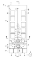
図1は本発明の第1の実施形態に係る検査システムの概略構成を示す平面図、図2は図1の検査システムのII−II′線による断面図であり、図3は図1の検査システムのIII-III′線による断面図である。
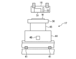
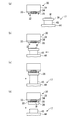
まず、FOUP18から検査前のウエハWをローダ21により取り出し、プリアライメント部24またはバッファ部25に搬送し、プリアライメント部24でプリアライメントを行ったウエハWについて、プリアライメント部24またはバッファ部25から搬送機構15により、ウエハWを搬送すべき検査ユニット30に搬送し、アライナー17上のチャックトップ36の上に載置する(図9(a))。このとき、アライナー17を移動させながら、カメラユニット16のアライメント用のカメラ51でウエハWを撮影する。なお、チャックトップ36にウエハWを載置する前の適宜のタイミングで、放射温度計52によりチャックトップ36表面の複数点の温度を測定しておく。
次に、第2の実施形態について説明する。
図12は、第2の実施形態に係る検査システムを示す平面図である。本実施形態の検査システム10′は、第1の実施形態の検査システム10とは異なり、X方向に沿って複数(図では5つ以上)の検査ユニット30が配置された検査ユニット列がZ方向(上下方向)に3段に配置された検査部12aと、これらの各段の側方にX方向に沿って延びる3つの搬送路14のみを含む検査領域12′を有しており、検査領域12′には第2の検査部12bが存在しない。他の構成は、第1の実施形態の検査システム10と同様である。
次に、第3の実施形態について説明する。
図13は、第3の実施形態に係る検査システムを示す平面図である。本実施形態の検査システム10″は、第1の実施形態の検査システム10とは異なり、第1の検査部12aと第2の検査部12bの間の搬送路14′の各段にX方向に沿って移動する搬送機構15が2つ設けられた検査領域12″を有している。一方の搬送機構15は第1の検査部12a専用であり、他方の搬送機構15は第2の検査部12b専用である。
なお、本発明は上記実施の形態に限定されることなく、本発明の思想の範囲内において種々変形可能である。
例えば、上記実施の形態では、アライナーと搬送機構とを別個に設けた例を示したが、アライナーにチャックトップを装着した状態で搬送ステージを構成し、搬送ステージがアライナーの機能と搬送機構の機能を兼備するようにしてもよい。
11;筐体
12,12′,12″;検査領域
13;ローダ領域
14,14′;搬送路
15;搬送機構
16;カメラユニット
17;アライナー
18;FOUP
21;ローダ
30;検査ユニット
70;制御部
W;ウエハ(被検査体)
Claims (10)
- 被検査体の電気的検査を行うためのテスタと、前記テスタと被検査体の間に設けられるプローブカードとを有し、被検査体の電気的検査を行う、複数の検査ユニットを有する検査部を備えた検査領域と、
被検査体の収容容器が配置される配置部と、前記収容容器と前記検査領域との間で被検査体の受け渡しを行うローダとを有するローダ領域と
を備え、
前記検査部は、前記検査ユニットが水平方向の一方向に複数配列されて形成された検査ユニット列が、垂直方向に複数段配置されて構成され、
前記配置部は、前記検査部の前記一方向の端部側に設けられ、
前記検査領域は、前記検査部の前記検査ユニット列の各段に隣接して設けられ、前記一方向に延びる複数の搬送路と、前記各搬送路に沿って移動可能に設けられ、前記ローダから搬入された被検査体を前記検査ユニットとの間で受け渡す複数の搬送機構とをさらに有し、
前記ローダ領域の前記配置部は、前記検査ユニットの配列方向に直交する方向に前記収容容器が複数配列されることを特徴とする検査システム。 - 前記検査領域は、前記搬送路を挟んで前記検査部と反対側に、前記検査ユニットを、垂直方向に複数段設け、その複数段の前記検査ユニットを水平方向の前記一方向に複数配列した他の検査部をさらに有することを特徴とする請求項1に記載の検査システム。
- 被検査体の電気的検査を行うためのテスタと、前記テスタと被検査体の間に設けられるプローブカードとを有し、被検査体の電気的検査を行う、複数の検査ユニットを有し、前記検査ユニットが水平方向の一方向に複数配列されて形成された検査ユニット列が、垂直方向に複数段配置されて構成され、それぞれが間隔を空けて対向するように設けられた2つの検査部と、
前記2つの検査部の各段の前記検査ユニット列の間に設けられ、前記一方向に延びる複数の搬送路と、
前記各搬送路に沿って移動可能に設けられ、前記各段の前記検査ユニット列の前記検査ユニットとの間で被検査体を受け渡す複数の搬送機構と
を有し、
前記2つの検査部と、前記搬送路と、前記搬送機構とは、検査領域を構成し、
被検査収容容器が配置される配置部と、前記収容容器と前記検査領域との間で被検査体の受け渡しを行うローダとを有するローダ領域をさらに有し、
前記配置部は、前記2つの検査部の前記一方向の端部側に設けられ、
前記ローダ領域の前記配置部は、前記検査ユニットの配列方向に直交する方向に前記収容容器が複数配列されることを特徴とする検査システム。 - 前記各搬送路に沿って2つの搬送機構が移動可能に設けられ、前記搬送機構の一方が、前記2つの検査部の一方に属する前記検査ユニットに対して被検査体の受け渡しを行い、前記搬送機構の他方が、前記2つの検査部の他方に属する検査ユニットに対して被検査体の受け渡しを行うことを特徴とする請求項2または請求項3に記載の検査システム。
- 前記検査部の前記検査ユニット列の各段に設けられ、ステージに載せられた被検査体を前記検査ユニットの前記プローブカードに対して位置決めするアライナーをさらに有することを特徴とする請求項1から請求項4のいずれか1項に記載の検査システム。
- 前記アライナーは、前記1つまたは2つの検査部の各段における全ての前記検査ユニットにアクセス可能に設けられていることを特徴とする請求項5に記載の検査システム。
- 前記検査ユニットは、検査時に、前記ステージ上の被検査体が前記プローブカードのプローブに接触した状態で、前記ステージが吸着されるように構成され、前記アライナーは、一の前記検査ユニットにおいて、前記ステージを上昇させて前記被検査体を前記プローブに接触させ、前記ステージを吸着させた後、一の前記検査ユニットから検査が終了した他の前記検査ユニットに移動し、その検査ユニットの前記ステージの取り外し動作を実施することを特徴とする請求項5または請求項6に記載の検査システム。
- 前記搬送路に沿って移動可能に設けられ、前記ステージに載せられた被検査体のアライメント用のカメラを有するカメラユニットをさらに有することを特徴とする請求項5から請求項7のいずれか1項に記載の検査システム。
- 前記カメラユニットは、前記ステージ上の基板の温度を測定する放射温度計を有することを特徴とする請求項8に記載の検査システム。
- 前記カメラユニットは、前記搬送機構と共通のガイドレールに沿って前記搬送路を移動可能に設けられていることを特徴とする請求項8または請求項9に記載の検査システム。
Priority Applications (6)
| Application Number | Priority Date | Filing Date | Title |
|---|---|---|---|
| JP2017139936A JP6887332B2 (ja) | 2017-07-19 | 2017-07-19 | 検査システム |
| PCT/JP2018/018314 WO2019017050A1 (ja) | 2017-07-19 | 2018-05-11 | 検査システム |
| KR1020207004705A KR102413295B1 (ko) | 2017-07-19 | 2018-05-11 | 검사 시스템 |
| US16/630,606 US11067624B2 (en) | 2017-07-19 | 2018-05-11 | Inspection system |
| TW107124558A TWI761555B (zh) | 2017-07-19 | 2018-07-17 | 檢查系統 |
| JP2021079077A JP2021119638A (ja) | 2017-07-19 | 2021-05-07 | 検査システム |
Applications Claiming Priority (1)
| Application Number | Priority Date | Filing Date | Title |
|---|---|---|---|
| JP2017139936A JP6887332B2 (ja) | 2017-07-19 | 2017-07-19 | 検査システム |
Related Child Applications (1)
| Application Number | Title | Priority Date | Filing Date |
|---|---|---|---|
| JP2021079077A Division JP2021119638A (ja) | 2017-07-19 | 2021-05-07 | 検査システム |
Publications (3)
| Publication Number | Publication Date |
|---|---|
| JP2019021804A JP2019021804A (ja) | 2019-02-07 |
| JP2019021804A5 JP2019021804A5 (ja) | 2020-04-30 |
| JP6887332B2 true JP6887332B2 (ja) | 2021-06-16 |
Family
ID=65015135
Family Applications (2)
| Application Number | Title | Priority Date | Filing Date |
|---|---|---|---|
| JP2017139936A Active JP6887332B2 (ja) | 2017-07-19 | 2017-07-19 | 検査システム |
| JP2021079077A Pending JP2021119638A (ja) | 2017-07-19 | 2021-05-07 | 検査システム |
Family Applications After (1)
| Application Number | Title | Priority Date | Filing Date |
|---|---|---|---|
| JP2021079077A Pending JP2021119638A (ja) | 2017-07-19 | 2021-05-07 | 検査システム |
Country Status (5)
| Country | Link |
|---|---|
| US (1) | US11067624B2 (ja) |
| JP (2) | JP6887332B2 (ja) |
| KR (1) | KR102413295B1 (ja) |
| TW (1) | TWI761555B (ja) |
| WO (1) | WO2019017050A1 (ja) |
Families Citing this family (12)
| Publication number | Priority date | Publication date | Assignee | Title |
|---|---|---|---|---|
| JP6785375B2 (ja) * | 2017-06-21 | 2020-11-18 | 東京エレクトロン株式会社 | 検査システム |
| JP7274350B2 (ja) * | 2019-05-28 | 2023-05-16 | 東京エレクトロン株式会社 | 搬送システム、検査システム及び検査方法 |
| TWI797461B (zh) * | 2019-07-26 | 2023-04-01 | 日商新川股份有限公司 | 封裝裝置 |
| CN113053774A (zh) * | 2019-12-27 | 2021-06-29 | 迪科特测试科技(苏州)有限公司 | 探测装置 |
| JP7390934B2 (ja) * | 2020-03-03 | 2023-12-04 | 東京エレクトロン株式会社 | 検査装置 |
| US20230221344A1 (en) * | 2020-06-02 | 2023-07-13 | Kawasaki Jukogyo Kabushiki Kaisha | Testing System |
| DE112021007343T5 (de) * | 2021-03-23 | 2024-05-02 | Kioxia Corporation | Speichersystem |
| JP7784890B2 (ja) * | 2021-12-27 | 2025-12-12 | 東京エレクトロン株式会社 | 検査装置及び検査方法 |
| JP2024020816A (ja) * | 2022-08-02 | 2024-02-15 | 東京エレクトロン株式会社 | 検査システム |
| JP2025082689A (ja) * | 2023-11-17 | 2025-05-29 | 東京エレクトロン株式会社 | 搬送システム、および搬送方法 |
| WO2025243755A1 (ja) * | 2024-05-22 | 2025-11-27 | 川崎重工業株式会社 | 基板搬送システム |
| JP7668407B1 (ja) * | 2024-05-22 | 2025-04-24 | 川崎重工業株式会社 | 基板搬送システム |
Family Cites Families (17)
| Publication number | Priority date | Publication date | Assignee | Title |
|---|---|---|---|---|
| JPS63229836A (ja) * | 1987-03-19 | 1988-09-26 | Nikon Corp | ウエハ検査装置 |
| JP2952331B2 (ja) | 1990-04-05 | 1999-09-27 | 東京エレクトロン株式会社 | プローブ装置 |
| JP3312748B2 (ja) * | 1992-06-05 | 2002-08-12 | 株式会社東京精密 | ウエハ検査装置及びウエハ検査方法 |
| JPH08335614A (ja) * | 1995-06-08 | 1996-12-17 | Tokyo Electron Ltd | プロ−ブシステム |
| KR20100084607A (ko) * | 2007-05-15 | 2010-07-27 | 로널드 씨 슈버트 | 웨이퍼 프로브 테스트 및 검사 시스템 |
| CN101689522B (zh) * | 2007-06-29 | 2011-11-02 | 爱德万测试株式会社 | 测试装置 |
| KR100892756B1 (ko) * | 2007-12-27 | 2009-04-15 | 세메스 주식회사 | 기판 처리 장치 및 이를 이용한 기판 이송 방법 |
| JP5139253B2 (ja) * | 2008-12-18 | 2013-02-06 | 東京エレクトロン株式会社 | 真空処理装置及び真空搬送装置 |
| CN102301462A (zh) * | 2009-02-12 | 2011-12-28 | 株式会社爱德万测试 | 半导体晶片测试装置 |
| JP2011009362A (ja) * | 2009-06-24 | 2011-01-13 | Tokyo Electron Ltd | インプリントシステム、インプリント方法、プログラム及びコンピュータ記憶媒体 |
| JP5952645B2 (ja) * | 2012-06-06 | 2016-07-13 | 東京エレクトロン株式会社 | ウエハ検査用インターフェース及びウエハ検査装置 |
| JP5918682B2 (ja) * | 2012-10-09 | 2016-05-18 | 東京エレクトロン株式会社 | プローブカード取り付け方法 |
| JP5690321B2 (ja) * | 2012-11-29 | 2015-03-25 | 株式会社アドバンテスト | プローブ装置および試験装置 |
| JP5718379B2 (ja) * | 2013-01-15 | 2015-05-13 | 東京エレクトロン株式会社 | 基板収納処理装置及び基板収納処理方法並びに基板収納処理用記憶媒体 |
| JP6333112B2 (ja) * | 2014-08-20 | 2018-05-30 | 東京エレクトロン株式会社 | ウエハ検査装置 |
| JP6418394B2 (ja) * | 2015-02-27 | 2018-11-07 | 株式会社東京精密 | プローバ及びプローブカードのプリヒート方法 |
| JP6652361B2 (ja) * | 2015-09-30 | 2020-02-19 | 東京エレクトロン株式会社 | ウエハ検査装置及びウエハ検査方法 |
-
2017
- 2017-07-19 JP JP2017139936A patent/JP6887332B2/ja active Active
-
2018
- 2018-05-11 KR KR1020207004705A patent/KR102413295B1/ko active Active
- 2018-05-11 US US16/630,606 patent/US11067624B2/en active Active
- 2018-05-11 WO PCT/JP2018/018314 patent/WO2019017050A1/ja not_active Ceased
- 2018-07-17 TW TW107124558A patent/TWI761555B/zh active
-
2021
- 2021-05-07 JP JP2021079077A patent/JP2021119638A/ja active Pending
Also Published As
| Publication number | Publication date |
|---|---|
| TW201909301A (zh) | 2019-03-01 |
| TWI761555B (zh) | 2022-04-21 |
| KR102413295B1 (ko) | 2022-06-27 |
| US20200158775A1 (en) | 2020-05-21 |
| JP2021119638A (ja) | 2021-08-12 |
| KR20200033288A (ko) | 2020-03-27 |
| WO2019017050A1 (ja) | 2019-01-24 |
| JP2019021804A (ja) | 2019-02-07 |
| US11067624B2 (en) | 2021-07-20 |
Similar Documents
| Publication | Publication Date | Title |
|---|---|---|
| JP6887332B2 (ja) | 検査システム | |
| CN101271858B (zh) | 检查装置 | |
| KR101208137B1 (ko) | 프로브 장치 | |
| JP7018784B2 (ja) | コンタクト精度保証方法および検査装置 | |
| JP2019021804A5 (ja) | ||
| KR102355572B1 (ko) | 검사 장치, 검사 시스템, 및 위치 맞춤 방법 | |
| KR102311129B1 (ko) | 검사 시스템 및 검사 시스템에 있어서의 온도 측정 방법 | |
| CN112394207B (zh) | 探针装置和探针卡的预冷却方法 | |
| CN110211889A (zh) | 检查系统 | |
| JP2021005686A (ja) | プローバおよびプローブカードのプリヒート方法 | |
| CN111446183A (zh) | 卡盘顶、检查装置以及卡盘顶的回收方法 | |
| CN102116835A (zh) | 探测装置以及衬底运送方法 | |
| TW201812948A (zh) | 電子零件搬送裝置及電子零件檢查裝置 | |
| JP4910033B2 (ja) | プローブ装置 | |
| JP4913201B2 (ja) | 基板搬送方法 | |
| US20250276848A1 (en) | Substrate processing apparatus and substrate processing method | |
| JP4402011B2 (ja) | 基板の処理システム及び基板の処理方法 | |
| JPWO2009107231A1 (ja) | 電子部品移載装置およびそれを備えた電子部品試験装置 | |
| KR20170094090A (ko) | 기판 검사 장치 및 기판 검사 방법 | |
| TWI398638B (zh) | A method of removing the electronic component, and a control program for carrying out the method | |
| JP2006126063A (ja) | 半導体検査装置およびicソケット | |
| TW202443748A (zh) | 工件搬運裝置及工件檢查裝置 | |
| JPH02256253A (ja) | 半導体検査装置 | |
| JP2011108832A (ja) | プローブ装置 | |
| JPH02311773A (ja) | 半導体検査方法 |
Legal Events
| Date | Code | Title | Description |
|---|---|---|---|
| A521 | Request for written amendment filed |
Free format text: JAPANESE INTERMEDIATE CODE: A523 Effective date: 20200316 |
|
| A621 | Written request for application examination |
Free format text: JAPANESE INTERMEDIATE CODE: A621 Effective date: 20200316 |
|
| TRDD | Decision of grant or rejection written | ||
| A01 | Written decision to grant a patent or to grant a registration (utility model) |
Free format text: JAPANESE INTERMEDIATE CODE: A01 Effective date: 20210420 |
|
| A61 | First payment of annual fees (during grant procedure) |
Free format text: JAPANESE INTERMEDIATE CODE: A61 Effective date: 20210518 |
|
| R150 | Certificate of patent or registration of utility model |
Ref document number: 6887332 Country of ref document: JP Free format text: JAPANESE INTERMEDIATE CODE: R150 |
|
| R250 | Receipt of annual fees |
Free format text: JAPANESE INTERMEDIATE CODE: R250 |
|
| R250 | Receipt of annual fees |
Free format text: JAPANESE INTERMEDIATE CODE: R250 |
|
| R250 | Receipt of annual fees |
Free format text: JAPANESE INTERMEDIATE CODE: R250 |