JP6899366B2 - 液晶表示装置 - Google Patents
液晶表示装置 Download PDFInfo
- Publication number
- JP6899366B2 JP6899366B2 JP2018224266A JP2018224266A JP6899366B2 JP 6899366 B2 JP6899366 B2 JP 6899366B2 JP 2018224266 A JP2018224266 A JP 2018224266A JP 2018224266 A JP2018224266 A JP 2018224266A JP 6899366 B2 JP6899366 B2 JP 6899366B2
- Authority
- JP
- Japan
- Prior art keywords
- liquid crystal
- image signal
- crystal panel
- unit
- output
- Prior art date
- Legal status (The legal status is an assumption and is not a legal conclusion. Google has not performed a legal analysis and makes no representation as to the accuracy of the status listed.)
- Active
Links
Images







Classifications
-
- G—PHYSICS
- G09—EDUCATION; CRYPTOGRAPHY; DISPLAY; ADVERTISING; SEALS
- G09G—ARRANGEMENTS OR CIRCUITS FOR CONTROL OF INDICATING DEVICES USING STATIC MEANS TO PRESENT VARIABLE INFORMATION
- G09G3/00—Control arrangements or circuits, of interest only in connection with visual indicators other than cathode-ray tubes
- G09G3/20—Control arrangements or circuits, of interest only in connection with visual indicators other than cathode-ray tubes for presentation of an assembly of a number of characters, e.g. a page, by composing the assembly by combination of individual elements arranged in a matrix no fixed position being assigned to or needed to be assigned to the individual characters or partial characters
- G09G3/34—Control arrangements or circuits, of interest only in connection with visual indicators other than cathode-ray tubes for presentation of an assembly of a number of characters, e.g. a page, by composing the assembly by combination of individual elements arranged in a matrix no fixed position being assigned to or needed to be assigned to the individual characters or partial characters by control of light from an independent source
- G09G3/36—Control arrangements or circuits, of interest only in connection with visual indicators other than cathode-ray tubes for presentation of an assembly of a number of characters, e.g. a page, by composing the assembly by combination of individual elements arranged in a matrix no fixed position being assigned to or needed to be assigned to the individual characters or partial characters by control of light from an independent source using liquid crystals
- G09G3/3607—Control arrangements or circuits, of interest only in connection with visual indicators other than cathode-ray tubes for presentation of an assembly of a number of characters, e.g. a page, by composing the assembly by combination of individual elements arranged in a matrix no fixed position being assigned to or needed to be assigned to the individual characters or partial characters by control of light from an independent source using liquid crystals for displaying colours or for displaying grey scales with a specific pixel layout, e.g. using sub-pixels
-
- G—PHYSICS
- G09—EDUCATION; CRYPTOGRAPHY; DISPLAY; ADVERTISING; SEALS
- G09G—ARRANGEMENTS OR CIRCUITS FOR CONTROL OF INDICATING DEVICES USING STATIC MEANS TO PRESENT VARIABLE INFORMATION
- G09G5/00—Control arrangements or circuits for visual indicators common to cathode-ray tube indicators and other visual indicators
- G09G5/02—Control arrangements or circuits for visual indicators common to cathode-ray tube indicators and other visual indicators characterised by the way in which colour is displayed
- G09G5/028—Circuits for converting colour display signals into monochrome display signals
-
- G—PHYSICS
- G09—EDUCATION; CRYPTOGRAPHY; DISPLAY; ADVERTISING; SEALS
- G09G—ARRANGEMENTS OR CIRCUITS FOR CONTROL OF INDICATING DEVICES USING STATIC MEANS TO PRESENT VARIABLE INFORMATION
- G09G5/00—Control arrangements or circuits for visual indicators common to cathode-ray tube indicators and other visual indicators
- G09G5/02—Control arrangements or circuits for visual indicators common to cathode-ray tube indicators and other visual indicators characterised by the way in which colour is displayed
- G09G5/06—Control arrangements or circuits for visual indicators common to cathode-ray tube indicators and other visual indicators characterised by the way in which colour is displayed using colour palettes, e.g. look-up tables
-
- G—PHYSICS
- G09—EDUCATION; CRYPTOGRAPHY; DISPLAY; ADVERTISING; SEALS
- G09G—ARRANGEMENTS OR CIRCUITS FOR CONTROL OF INDICATING DEVICES USING STATIC MEANS TO PRESENT VARIABLE INFORMATION
- G09G2300/00—Aspects of the constitution of display devices
- G09G2300/02—Composition of display devices
- G09G2300/023—Display panel composed of stacked panels
-
- G—PHYSICS
- G09—EDUCATION; CRYPTOGRAPHY; DISPLAY; ADVERTISING; SEALS
- G09G—ARRANGEMENTS OR CIRCUITS FOR CONTROL OF INDICATING DEVICES USING STATIC MEANS TO PRESENT VARIABLE INFORMATION
- G09G2310/00—Command of the display device
- G09G2310/08—Details of timing specific for flat panels, other than clock recovery
-
- G—PHYSICS
- G09—EDUCATION; CRYPTOGRAPHY; DISPLAY; ADVERTISING; SEALS
- G09G—ARRANGEMENTS OR CIRCUITS FOR CONTROL OF INDICATING DEVICES USING STATIC MEANS TO PRESENT VARIABLE INFORMATION
- G09G2320/00—Control of display operating conditions
- G09G2320/02—Improving the quality of display appearance
- G09G2320/0209—Crosstalk reduction, i.e. to reduce direct or indirect influences of signals directed to a certain pixel of the displayed image on other pixels of said image, inclusive of influences affecting pixels in different frames or fields or sub-images which constitute a same image, e.g. left and right images of a stereoscopic display
-
- G—PHYSICS
- G09—EDUCATION; CRYPTOGRAPHY; DISPLAY; ADVERTISING; SEALS
- G09G—ARRANGEMENTS OR CIRCUITS FOR CONTROL OF INDICATING DEVICES USING STATIC MEANS TO PRESENT VARIABLE INFORMATION
- G09G2320/00—Control of display operating conditions
- G09G2320/02—Improving the quality of display appearance
- G09G2320/0233—Improving the luminance or brightness uniformity across the screen
-
- G—PHYSICS
- G09—EDUCATION; CRYPTOGRAPHY; DISPLAY; ADVERTISING; SEALS
- G09G—ARRANGEMENTS OR CIRCUITS FOR CONTROL OF INDICATING DEVICES USING STATIC MEANS TO PRESENT VARIABLE INFORMATION
- G09G2320/00—Control of display operating conditions
- G09G2320/02—Improving the quality of display appearance
- G09G2320/0271—Adjustment of the gradation levels within the range of the gradation scale, e.g. by redistribution or clipping
-
- G—PHYSICS
- G09—EDUCATION; CRYPTOGRAPHY; DISPLAY; ADVERTISING; SEALS
- G09G—ARRANGEMENTS OR CIRCUITS FOR CONTROL OF INDICATING DEVICES USING STATIC MEANS TO PRESENT VARIABLE INFORMATION
- G09G2320/00—Control of display operating conditions
- G09G2320/02—Improving the quality of display appearance
- G09G2320/0271—Adjustment of the gradation levels within the range of the gradation scale, e.g. by redistribution or clipping
- G09G2320/0276—Adjustment of the gradation levels within the range of the gradation scale, e.g. by redistribution or clipping for the purpose of adaptation to the characteristics of a display device, i.e. gamma correction
-
- G—PHYSICS
- G09—EDUCATION; CRYPTOGRAPHY; DISPLAY; ADVERTISING; SEALS
- G09G—ARRANGEMENTS OR CIRCUITS FOR CONTROL OF INDICATING DEVICES USING STATIC MEANS TO PRESENT VARIABLE INFORMATION
- G09G2320/00—Control of display operating conditions
- G09G2320/02—Improving the quality of display appearance
- G09G2320/0285—Improving the quality of display appearance using tables for spatial correction of display data
Landscapes
- Engineering & Computer Science (AREA)
- Physics & Mathematics (AREA)
- Computer Hardware Design (AREA)
- General Physics & Mathematics (AREA)
- Theoretical Computer Science (AREA)
- Chemical & Material Sciences (AREA)
- Crystallography & Structural Chemistry (AREA)
- Liquid Crystal Display Device Control (AREA)
- Control Of Indicators Other Than Cathode Ray Tubes (AREA)
- Liquid Crystal (AREA)
- Devices For Indicating Variable Information By Combining Individual Elements (AREA)
Description
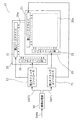
複数の液晶パネル(例えば、第1液晶パネル及び第2液晶パネル)を重ね合わせると、第1液晶パネルと第2液晶パネルとの間隔に応じて視差が発生して画像品位が低下する。そこで、視差を低減するための画像処理を行うことが検討されている。そのような液晶表示装置を、図18を参照しながら説明する。図18は、比較例に係る液晶表示装置1010の機能構成を示すブロック図である。
以下、本実施の形態に係る液晶表示装置について、図1〜図9を参照しながら説明する。
まず、実施の形態1に係る液晶表示装置10の全体の概略構成について、図1〜図5を参照しながら説明する。図1は、実施の形態1に係る液晶表示装置10の分解斜視図である。図2は、実施の形態1に係る液晶表示装置10の概略構成を示す図である。図2では、液晶表示装置10における第1液晶パネル20及び第2液晶パネル30のドライバの構成を示す。
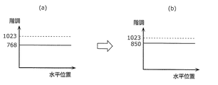
次に、上記の液晶表示装置10の動作について、図6〜図9を参照しながら説明する。図6は、実施の形態1に係る液晶表示装置10の動作を示すフローチャートである。図7は、実施の形態1に係る第1出力画像信号DAT1の生成を説明するための図である。
以上説明したように、液晶表示装置10は、第1液晶パネル20と、第1液晶パネル20の背面側において第1液晶パネル20と重ね合わせて配置される第2液晶パネル30とを有する液晶表示部10a(表示部の一例)と、入力画像信号Dataに基づいて、第1液晶パネル20に出力する第1出力画像信号DAT1と、第2液晶パネル30に出力する第2出力画像信号DAT2とを生成する画像処理部80とを備える。そして、画像処理部80は、入力画像信号Dataを、第1出力画像信号DAT1を生成するための第1分配画像信号と、第2出力画像信号DAT2を生成するための第2分配画像信号とに分配する分配部90と、分配部90から出力された第1分配画像信号に対して、液晶表示部10aの表示ムラを抑制する第1ムラ補正を行うことで第1出力画像信号DAT1を生成し、生成した第1出力画像信号DAT1を第1液晶パネル20に出力する表示ムラ補正部100(第1ムラ補正部の一例)とを有する。
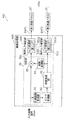
以下、本変形例に係る液晶表示装置110について、図10を参照しながら説明する。図10は、実施の形態1の変形例に係る液晶表示装置110の機能構成を示すブロック図である。なお、実施の形態1に係る液晶表示装置10との相違点を中心に説明し、同様の構成については同一の符号を付し、説明を省略又は簡略化する場合がある。
以下、本実施の形態に係る液晶表示装置について、図11〜図15を参照しながら説明する。
まず、実施の形態2に係る液晶表示装置210の全体の概略構成について、図11を参照しながら説明する。図11は、実施の形態2に係る液晶表示装置210の概略構成を示すブロック図である。なお、本実の形態では、実施の形態1に係る液晶表示装置10との相違点を中心に説明し、同様の構成については同一の符号を付し、説明を省略又は簡略化する場合がある。
次に、上記の液晶表示装置210の動作について、図12〜図15を参照しながら説明する。図12は、実施の形態2に係る液晶表示装置210の動作を示すフローチャートである。図13は、実施の形態2に係る第2出力画像信号DAT2の生成を説明するための図である。
以上説明したように、液晶表示装置210は、第1液晶パネル20と、第1液晶パネル20の背面側において第1液晶パネル20と重ね合わせて配置される第2液晶パネル30とを有する液晶表示部10a(表示部の一例)と、入力画像信号Dataに基づいて、第1液晶パネル20に出力する第1出力画像信号DAT1と、第2液晶パネル30に出力する第2出力画像信号DAT2とを生成する画像処理部280とを備える。そして、画像処理部280は、入力画像信号Dataを、第1出力画像信号DAT1と、第2出力画像信号DAT2を生成するための第2分配画像信号(分配画像信号の一例)とに分配する分配部90と、分配部90から出力された第2分配画像信号に対して、液晶表示部10aの表示ムラを抑制するムラ補正を行うことで第2出力画像信号DAT2を生成し、生成した第2出力画像信号DAT2を第2液晶パネル30に出力する表示ムラ補正部300(ムラ補正部の一例)とを有する。
以下、本変形例に係る液晶表示装置310について、図16を参照しながら説明する。図16は、実施の形態2の変形例に係る液晶表示装置310の機能構成を示すブロック図である。なお、実施の形態2に係る液晶表示装置210との相違点を中心に説明し、同様の構成については同一の符号を付し、説明を省略又は簡略化する場合がある。
以下、本実施の形態に係る液晶表示装置について、図17を参照しながら説明する。
まず、実施の形態3に係る液晶表示装置410の全体の概略構成について、図17を参照しながら説明する。図17は、実施の形態3に係る液晶表示装置410の機能構成を示すブロック図である。なお、実施の形態1に係る液晶表示装置10との相違点を中心に説明し、同様の構成については同一の符号を付し、説明を省略又は簡略化する場合がある。
以上のように、本実施の形態に係る液晶表示装置410は、分配部90から出力された第2分配画像信号に対して、液晶表示部10a(表示部の一例)の表示ムラを抑制する第2ムラ補正を行うことで第2出力画像信号DAT2を生成し、生成した第2出力画像信号DAT2を第2液晶パネル30に出力する表示ムラ補正部510(第2ムラ補正部の一例)を、さらに備える。
以上、各実施の形態及び変形例(以下において、実施の形態等とも記載する)に係る液晶表示装置について説明したが、本開示は、上記実施の形態に限定されるものではない。
10a 液晶表示部(表示部)
20 第1液晶パネル
20a 第1画像表示領域
21 第1ソースドライバ
22 第1ゲートドライバ
23 第1透明基板
23a 第1TFT基板
23b 第1対向基板
24 第1液晶層
25 第1偏光板
26 第1TFT層
27 第1画素形成層
27a 第1ブラックマトリクス
27b カラーフィルタ
30 第2液晶パネル
30a 第2画像表示領域
31 第2ソースドライバ
32 第2ゲートドライバ
33 第2透明基板
33a 第2TFT基板
33b 第2対向基板
34 第2液晶層
35 第2偏光板
36 第2TFT層
37 第2画素形成層
37a 第2ブラックマトリクス
40 接着層
50 バックライト
60 フロントシャーシ
71 第1タイミングコントローラ
72 第2タイミングコントローラ
80、180、280、380 画像処理部
90 分配部
91 白黒画像生成部
92 ガンマ処理部(階調補正部)
93 視差低減部
94 除算処理部
95 乗算器
100、200、300、400、500、510 表示ムラ補正部
101、301、501、511 ムラ処理部
101a、301a、501a 第1ルックアップテーブル
101b、301b、511a 第2ルックアップテーブル
202、402 信号予測部
Data 入力画像信号
DAT1 第1出力画像信号
DAT2 第2出力画像信号
Claims (9)
- 第1液晶パネルと、前記第1液晶パネルの背面側において前記第1液晶パネルと重ね合わせて配置される第2液晶パネルとを有する表示部と、
入力画像信号に基づいて、前記第1液晶パネルに出力する第1出力画像信号と、前記第2液晶パネルに出力する第2出力画像信号とを生成する画像処理部とを備え、
前記画像処理部は、
前記入力画像信号を、前記第1出力画像信号を生成するための第1分配画像信号と、前記第2出力画像信号を生成するための第2分配画像信号とに分配する分配部と、
前記分配部から出力された前記第1分配画像信号に対して、前記表示部の表示ムラを抑制する第1ムラ補正を行うことで前記第1出力画像信号を生成し、生成した前記第1出力画像信号を前記第1液晶パネルに出力する第1ムラ補正部とを有し、
前記分配部は、前記第2分配画像信号を前記第2出力画像信号として前記第2液晶パネルに出力し、
前記第1ムラ補正部は、前記入力画像信号に基づいて前記第2出力画像信号を予測する予測部をさらに有し、前記予測部が予測した信号に基づいて前記第1分配画像信号に対して前記第1ムラ補正を行う
液晶表示装置。 - 前記第1ムラ補正部は、前記第1液晶パネルの表示ムラを抑制するための第1ルックアップテーブルと、前記第2液晶パネルの表示ムラを抑制するための第2ルックアップテーブルとを有し、前記第1ルックアップテーブル及び前記第2ルックアップテーブルを用いて、前記第1分配画像信号に対して前記第1ムラ補正を行う
請求項1に記載の液晶表示装置。 - 前記分配部から出力された前記第2分配画像信号に対して、前記表示部の表示ムラを抑制する第2ムラ補正を行うことで前記第2出力画像信号を生成し、生成した前記第2出力画像信号を前記第2液晶パネルに出力する第2ムラ補正部を、さらに備える
請求項1に記載の液晶表示装置。 - 前記第1ムラ補正部は、前記第1液晶パネルの表示ムラを抑制するための第1ルックアップテーブルを有し、当該第1ルックアップテーブルを用いて前記第1ムラ補正を行い、
前記第2ムラ補正部は、前記第2液晶パネルの表示ムラを抑制するための第2ルックアップテーブルを有し、当該第2ルックアップテーブルを用いて前記第2ムラ補正を行う
請求項3に記載の液晶表示装置。 - 第1液晶パネルと、前記第1液晶パネルの背面側において前記第1液晶パネルと重ね合わせて配置される第2液晶パネルとを有する表示部と、
入力画像信号に基づいて、前記第1液晶パネルに出力する第1出力画像信号と、前記第2液晶パネルに出力する第2出力画像信号とを生成する画像処理部とを備え、
前記画像処理部は、
前記入力画像信号を、前記第1出力画像信号と、前記第2出力画像信号を生成するための分配画像信号とに分配する分配部と、
前記分配部から出力された前記分配画像信号に対して、前記表示部の表示ムラを抑制するムラ補正を行うことで前記第2出力画像信号を生成し、生成した前記第2出力画像信号を前記第2液晶パネルに出力するムラ補正部とを有し、
前記分配部は、前記分配画像信号を前記第1出力画像信号として前記第1液晶パネルに出力し、
前記ムラ補正部は、前記入力画像信号に基づいて前記第1出力画像信号を予測する予測部をさらに有し、前記予測部が予測した信号に基づいて前記分配画像信号に対して前記ムラ補正を行う
液晶表示装置。 - 前記ムラ補正部は、前記第1液晶パネルの表示ムラを抑制するための第1ルックアップテーブルと、前記第2液晶パネルの表示ムラを抑制するための第2ルックアップテーブルとを有し、前記第1ルックアップテーブル及び前記第2ルックアップテーブルを用いて、前記分配画像信号に対して前記ムラ補正を行う
請求項5に記載の液晶表示装置。 - 前記分配部は、前記入力画像信号に含まれる複数の階調値のうち第1階調値以上の階調値を第2階調値に階調補正をする階調補正部と、
前記階調補正部が出力した前記階調補正をした前記入力画像信号に対して、前記第1出力画像信号に基づく第1画像と、前記第2出力画像信号に基づく第2画像との視差を低減する補正をする視差低減部とを有する
請求項1〜6のいずれか1項に記載の液晶表示装置。 - 前記第2階調値は、前記階調補正部が出力可能な最大階調値より小さい値である
請求項7に記載の液晶表示装置。 - 前記第1液晶パネルは、カラー画像を表示し、
前記第2液晶パネルは、モノクロ画像を表示する
請求項1〜8のいずれか1項に記載の液晶表示装置。
Priority Applications (3)
| Application Number | Priority Date | Filing Date | Title |
|---|---|---|---|
| JP2018224266A JP6899366B2 (ja) | 2018-11-29 | 2018-11-29 | 液晶表示装置 |
| US16/691,274 US11114049B2 (en) | 2018-11-29 | 2019-11-21 | Liquid crystal display device |
| CN201911179813.0A CN111243536B (zh) | 2018-11-29 | 2019-11-26 | 液晶显示装置 |
Applications Claiming Priority (1)
| Application Number | Priority Date | Filing Date | Title |
|---|---|---|---|
| JP2018224266A JP6899366B2 (ja) | 2018-11-29 | 2018-11-29 | 液晶表示装置 |
Publications (2)
| Publication Number | Publication Date |
|---|---|
| JP2020086321A JP2020086321A (ja) | 2020-06-04 |
| JP6899366B2 true JP6899366B2 (ja) | 2021-07-07 |
Family
ID=70849237
Family Applications (1)
| Application Number | Title | Priority Date | Filing Date |
|---|---|---|---|
| JP2018224266A Active JP6899366B2 (ja) | 2018-11-29 | 2018-11-29 | 液晶表示装置 |
Country Status (3)
| Country | Link |
|---|---|
| US (1) | US11114049B2 (ja) |
| JP (1) | JP6899366B2 (ja) |
| CN (1) | CN111243536B (ja) |
Families Citing this family (4)
| Publication number | Priority date | Publication date | Assignee | Title |
|---|---|---|---|---|
| JP7359687B2 (ja) * | 2019-12-25 | 2023-10-11 | パナソニック インテレクチュアル プロパティ コーポレーション オブ アメリカ | 液晶表示装置 |
| US11605358B2 (en) * | 2021-03-12 | 2023-03-14 | Sharp Kabushiki Kaisha | Liquid crystal display including two overlapping display panels that differ from each other in terms of the size of their respective display pixels |
| US11887518B2 (en) * | 2022-01-06 | 2024-01-30 | Sharp Kabushiki Kaisha | Display device having displayable area expansion unit and cutting unit and control method thereof |
| US12315468B2 (en) * | 2022-02-14 | 2025-05-27 | Sharp Kabushiki Kaisha | Display device and display method |
Family Cites Families (8)
| Publication number | Priority date | Publication date | Assignee | Title |
|---|---|---|---|---|
| WO2007040127A1 (ja) * | 2005-09-30 | 2007-04-12 | Sharp Kabushiki Kaisha | 液晶表示装置およびテレビジョン受信機 |
| JP4870151B2 (ja) * | 2006-03-22 | 2012-02-08 | シャープ株式会社 | 液晶表示装置およびテレビジョン受信機 |
| JP2008122536A (ja) * | 2006-11-09 | 2008-05-29 | Sharp Corp | 液晶表示装置、液晶表示装置の駆動方法、およびテレビジョン受信機 |
| JP2008145981A (ja) * | 2006-12-13 | 2008-06-26 | Sharp Corp | 液晶表示装置、その駆動方法、及びテレビジョン受信機 |
| CN101981497B (zh) * | 2008-04-01 | 2013-06-19 | 皇家飞利浦电子股份有限公司 | 具有可调节白色点的高对比度液晶显示器 |
| JP5382498B2 (ja) * | 2008-11-10 | 2014-01-08 | Nltテクノロジー株式会社 | 液晶表示装置、液晶表示制御装置、電子機器、および液晶表示装置の駆動方法 |
| WO2014119403A1 (ja) * | 2013-01-30 | 2014-08-07 | ソニー株式会社 | 表示制御装置および方法 |
| JP2015152707A (ja) * | 2014-02-13 | 2015-08-24 | キヤノン株式会社 | 液晶表示装置およびその制御方法、制御プログラム |
-
2018
- 2018-11-29 JP JP2018224266A patent/JP6899366B2/ja active Active
-
2019
- 2019-11-21 US US16/691,274 patent/US11114049B2/en active Active
- 2019-11-26 CN CN201911179813.0A patent/CN111243536B/zh active Active
Also Published As
| Publication number | Publication date |
|---|---|
| CN111243536A (zh) | 2020-06-05 |
| JP2020086321A (ja) | 2020-06-04 |
| US20200175934A1 (en) | 2020-06-04 |
| CN111243536B (zh) | 2022-07-22 |
| US11114049B2 (en) | 2021-09-07 |
Similar Documents
| Publication | Publication Date | Title |
|---|---|---|
| CN107533834B (zh) | 使用局部化背光的显示器缺陷补偿 | |
| JP6899366B2 (ja) | 液晶表示装置 | |
| JP7246013B2 (ja) | 画像表示装置及び画像表示方法 | |
| JP5650422B2 (ja) | 液晶表示装置 | |
| US10553165B2 (en) | Method and apparatus for detecting high-frequency component in image | |
| WO2012147651A1 (ja) | マルチディスプレイ装置及び画像表示装置 | |
| CN113031353B (zh) | 液晶显示装置 | |
| US20110267541A1 (en) | Display apparatus | |
| US11328680B2 (en) | Image processing device and liquid crystal display device | |
| JP7646456B2 (ja) | 液晶表示装置 | |
| KR101906422B1 (ko) | 화질처리방법과 이를 이용한 표시장치 | |
| JP2012078373A (ja) | 表示装置の色度調整方法 | |
| US10789901B2 (en) | Liquid crystal display device | |
| US20210350753A1 (en) | Display device and driving method thereof | |
| US20200175946A1 (en) | Display device | |
| TWI756001B (zh) | 顯示裝置及其漏光補償方法 | |
| CN114765020B (zh) | 显示设备及其漏光补偿方法 | |
| JP2021076821A (ja) | 液晶表示装置 |
Legal Events
| Date | Code | Title | Description |
|---|---|---|---|
| A521 | Request for written amendment filed |
Free format text: JAPANESE INTERMEDIATE CODE: A523 Effective date: 20190926 |
|
| A621 | Written request for application examination |
Free format text: JAPANESE INTERMEDIATE CODE: A621 Effective date: 20191205 |
|
| A711 | Notification of change in applicant |
Free format text: JAPANESE INTERMEDIATE CODE: A711 Effective date: 20200501 |
|
| A977 | Report on retrieval |
Free format text: JAPANESE INTERMEDIATE CODE: A971007 Effective date: 20200930 |
|
| A131 | Notification of reasons for refusal |
Free format text: JAPANESE INTERMEDIATE CODE: A131 Effective date: 20201013 |
|
| A521 | Request for written amendment filed |
Free format text: JAPANESE INTERMEDIATE CODE: A523 Effective date: 20201211 |
|
| TRDD | Decision of grant or rejection written | ||
| A01 | Written decision to grant a patent or to grant a registration (utility model) |
Free format text: JAPANESE INTERMEDIATE CODE: A01 Effective date: 20210518 |
|
| A61 | First payment of annual fees (during grant procedure) |
Free format text: JAPANESE INTERMEDIATE CODE: A61 Effective date: 20210614 |
|
| R150 | Certificate of patent or registration of utility model |
Ref document number: 6899366 Country of ref document: JP Free format text: JAPANESE INTERMEDIATE CODE: R150 |
|
| S111 | Request for change of ownership or part of ownership |
Free format text: JAPANESE INTERMEDIATE CODE: R313117 |
|
| R350 | Written notification of registration of transfer |
Free format text: JAPANESE INTERMEDIATE CODE: R350 |
|
| R250 | Receipt of annual fees |
Free format text: JAPANESE INTERMEDIATE CODE: R250 |
|
| R250 | Receipt of annual fees |
Free format text: JAPANESE INTERMEDIATE CODE: R250 |