JP6900660B2 - シールド層を有するモジュール - Google Patents
シールド層を有するモジュール Download PDFInfo
- Publication number
- JP6900660B2 JP6900660B2 JP2016230368A JP2016230368A JP6900660B2 JP 6900660 B2 JP6900660 B2 JP 6900660B2 JP 2016230368 A JP2016230368 A JP 2016230368A JP 2016230368 A JP2016230368 A JP 2016230368A JP 6900660 B2 JP6900660 B2 JP 6900660B2
- Authority
- JP
- Japan
- Prior art keywords
- shield layer
- module
- wiring board
- electrode
- external terminal
- Prior art date
- Legal status (The legal status is an assumption and is not a legal conclusion. Google has not performed a legal analysis and makes no representation as to the accuracy of the status listed.)
- Active
Links
- 238000007789 sealing Methods 0.000 claims description 52
- 229920005989 resin Polymers 0.000 claims description 51
- 239000011347 resin Substances 0.000 claims description 51
- 239000004020 conductor Substances 0.000 claims description 14
- 230000002093 peripheral effect Effects 0.000 claims description 7
- 239000002184 metal Substances 0.000 description 19
- 229910052751 metal Inorganic materials 0.000 description 19
- 239000004065 semiconductor Substances 0.000 description 12
- 229910052802 copper Inorganic materials 0.000 description 8
- 238000000034 method Methods 0.000 description 7
- 230000000694 effects Effects 0.000 description 6
- 239000000758 substrate Substances 0.000 description 6
- 229910052709 silver Inorganic materials 0.000 description 5
- 229910000679 solder Inorganic materials 0.000 description 5
- 239000011159 matrix material Substances 0.000 description 4
- 230000015572 biosynthetic process Effects 0.000 description 3
- 238000000576 coating method Methods 0.000 description 3
- 239000003822 epoxy resin Substances 0.000 description 2
- 238000004519 manufacturing process Methods 0.000 description 2
- 238000005192 partition Methods 0.000 description 2
- 229920000647 polyepoxide Polymers 0.000 description 2
- 238000004544 sputter deposition Methods 0.000 description 2
- 238000007740 vapor deposition Methods 0.000 description 2
- 229910001218 Gallium arsenide Inorganic materials 0.000 description 1
- 230000002411 adverse Effects 0.000 description 1
- 239000003990 capacitor Substances 0.000 description 1
- 239000000919 ceramic Substances 0.000 description 1
- 238000000748 compression moulding Methods 0.000 description 1
- 239000011521 glass Substances 0.000 description 1
- 230000000873 masking effect Effects 0.000 description 1
- 238000012986 modification Methods 0.000 description 1
- 230000004048 modification Effects 0.000 description 1
- 238000007639 printing Methods 0.000 description 1
- 238000007650 screen-printing Methods 0.000 description 1
- 238000000638 solvent extraction Methods 0.000 description 1
- 238000001721 transfer moulding Methods 0.000 description 1
Images


Landscapes
- Non-Metallic Protective Coatings For Printed Circuits (AREA)
- Shielding Devices Or Components To Electric Or Magnetic Fields (AREA)
- Structure Of Printed Boards (AREA)
Description
この構成によれば、外部端子電極の配置面を除いて第1のシールド層で被覆するとともに、外部端子電極を隔離するよう外部端子電極の配置面を第2のシールド層で被覆している。このため、外部端子電極を第2のシールド層に電気的に接続しないようにしつつ、第1のシールド層が被覆していない領域からの電磁波の侵入および漏洩を第2のシールド層で軽減することができ、シールド層による電子部品に対するシールド特性の向上を図ることができる。また、ダミー電極の大きさを変えることにより、グランド電極と第2のシールド層との接触面積を調整することができる。
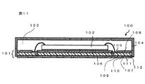
本発明の第1実施形態に係るモジュール1について、図1および図2を参照して説明する。なお、図1はモジュール1の底面図、図2は図1のA−A”断面図である。
次に、モジュール1の製造方法について説明する。
本発明の第2実施形態に係るモジュールについて、図3ないし図5を参照して説明する。なお、図3はシールド前のモジュール1aの底面図、図4はシールド後のモジュール1aの底面図、図5は図4のB−B”断面図である。
本発明の第3実施形態に係るモジュールについて、図6ないし図8を参照して説明する。なお、図6はシールド前のモジュール1bの底面図、図7はシールド後のモジュール1bの底面図、図8は図7のC−C”断面図である。
本発明の第4実施形態に係るモジュールについて、図9を参照して説明する。なお、図9はモジュール1cの断面図である。
本発明の第5実施形態に係るモジュールについて、図10を参照して説明する。なお、図10はモジュール1dの断面図である。
Claims (1)
- 一方主面と他方主面を有する配線基板と、
前記配線基板の一方主面と他方主面のうち、少なくとも一方主面に実装された電子部品と、
前記少なくとも一方主面と前記電子部品とを封止する封止樹脂層と、
外部端子電極と、
前記配線基板および前記封止樹脂層の前記外部端子電極の配置面以外の面を被覆する第1のシールド層と、
前記外部端子電極を隔離するよう前記外部端子電極の配置面を被覆する第2のシールド層と
を備え、
前記外部端子電極の配置面にはグランド電極およびダミー電極がさらに配置されており、
前記第2のシールド層は、前記外部端子電極の配置面のうちの前記ダミー電極の配置領域を被覆し、前記グランド電極の配置領域と当該配置領域の周辺領域とを被覆しておらず、
前記グランド電極と前記ダミー電極とを電気的に接続する接続導体をさらに備える
ことを特徴とするモジュール。
Priority Applications (1)
| Application Number | Priority Date | Filing Date | Title |
|---|---|---|---|
| JP2016230368A JP6900660B2 (ja) | 2016-11-28 | 2016-11-28 | シールド層を有するモジュール |
Applications Claiming Priority (1)
| Application Number | Priority Date | Filing Date | Title |
|---|---|---|---|
| JP2016230368A JP6900660B2 (ja) | 2016-11-28 | 2016-11-28 | シールド層を有するモジュール |
Publications (2)
| Publication Number | Publication Date |
|---|---|
| JP2018088460A JP2018088460A (ja) | 2018-06-07 |
| JP6900660B2 true JP6900660B2 (ja) | 2021-07-07 |
Family
ID=62494654
Family Applications (1)
| Application Number | Title | Priority Date | Filing Date |
|---|---|---|---|
| JP2016230368A Active JP6900660B2 (ja) | 2016-11-28 | 2016-11-28 | シールド層を有するモジュール |
Country Status (1)
| Country | Link |
|---|---|
| JP (1) | JP6900660B2 (ja) |
Families Citing this family (9)
| Publication number | Priority date | Publication date | Assignee | Title |
|---|---|---|---|---|
| JP7124795B2 (ja) | 2019-06-27 | 2022-08-24 | 株式会社村田製作所 | 電子部品モジュール、電子部品ユニット、および、電子部品モジュールの製造方法 |
| WO2021049521A1 (ja) | 2019-09-13 | 2021-03-18 | 株式会社村田製作所 | モジュール |
| CN114424333A (zh) | 2019-09-19 | 2022-04-29 | 株式会社村田制作所 | 模块 |
| CN114430937B (zh) * | 2019-09-27 | 2025-09-23 | 株式会社村田制作所 | 电子部件模块 |
| CN114846918B (zh) * | 2019-12-20 | 2025-07-08 | 株式会社村田制作所 | 电子部件模块以及电子部件模块的制造方法 |
| WO2021131775A1 (ja) * | 2019-12-27 | 2021-07-01 | 株式会社村田製作所 | モジュール |
| CN219395428U (zh) | 2020-06-16 | 2023-07-21 | 株式会社村田制作所 | 模块 |
| JP7567862B2 (ja) * | 2022-06-08 | 2024-10-16 | 株式会社村田製作所 | 回路基板及び回路モジュール |
| CN118335723A (zh) * | 2024-06-13 | 2024-07-12 | 成都嘉纳海威科技有限责任公司 | 一种高电磁隔离度的封装结构及制作方法 |
Family Cites Families (4)
| Publication number | Priority date | Publication date | Assignee | Title |
|---|---|---|---|---|
| CN101300911B (zh) * | 2005-11-28 | 2010-10-27 | 株式会社村田制作所 | 电路模块以及制造电路模块的方法 |
| JP2012159935A (ja) * | 2011-01-31 | 2012-08-23 | Murata Mfg Co Ltd | 電子部品モジュール、電子部品モジュールの製造方法、多機能カード |
| JP5622906B1 (ja) * | 2013-08-09 | 2014-11-12 | 太陽誘電株式会社 | 回路モジュールの製造方法 |
| CN107535078B (zh) * | 2015-05-20 | 2020-03-31 | 株式会社村田制作所 | 高频模块 |
-
2016
- 2016-11-28 JP JP2016230368A patent/JP6900660B2/ja active Active
Also Published As
| Publication number | Publication date |
|---|---|
| JP2018088460A (ja) | 2018-06-07 |
Similar Documents
| Publication | Publication Date | Title |
|---|---|---|
| JP6900660B2 (ja) | シールド層を有するモジュール | |
| JP6760397B2 (ja) | モジュール | |
| JP7120295B2 (ja) | 高周波モジュール | |
| US10667381B2 (en) | High frequency module | |
| JP6414637B2 (ja) | 高周波モジュール | |
| US10312172B2 (en) | High-frequency module | |
| US10674648B2 (en) | High-frequency module | |
| WO2018101384A1 (ja) | 高周波モジュール | |
| US20150235966A1 (en) | Wiring board and semiconductor device using the same | |
| JPWO2019167908A1 (ja) | 高周波モジュール | |
| WO2011086612A1 (ja) | 半導体装置 | |
| WO2017043621A1 (ja) | 高周波モジュール | |
| US9209053B2 (en) | Manufacturing method of a conductive shield layer in semiconductor device | |
| CN110610906A (zh) | 半导体电磁屏蔽结构及其制作方法 | |
| US11291108B2 (en) | Radio-frequency module with shield wall | |
| JP7130958B2 (ja) | モジュール | |
| US20220310317A1 (en) | Electronic component module | |
| US12293976B2 (en) | Semiconductor EMI shielding component, semiconductor package structure and manufacturing method thereof | |
| JP7131624B2 (ja) | モジュール | |
| JP6414639B2 (ja) | 高周波モジュールおよびその製造方法 |
Legal Events
| Date | Code | Title | Description |
|---|---|---|---|
| A621 | Written request for application examination |
Free format text: JAPANESE INTERMEDIATE CODE: A621 Effective date: 20190924 |
|
| A977 | Report on retrieval |
Free format text: JAPANESE INTERMEDIATE CODE: A971007 Effective date: 20200805 |
|
| A131 | Notification of reasons for refusal |
Free format text: JAPANESE INTERMEDIATE CODE: A131 Effective date: 20201006 |
|
| A521 | Written amendment |
Free format text: JAPANESE INTERMEDIATE CODE: A523 Effective date: 20201201 |
|
| TRDD | Decision of grant or rejection written | ||
| A01 | Written decision to grant a patent or to grant a registration (utility model) |
Free format text: JAPANESE INTERMEDIATE CODE: A01 Effective date: 20210518 |
|
| A61 | First payment of annual fees (during grant procedure) |
Free format text: JAPANESE INTERMEDIATE CODE: A61 Effective date: 20210531 |
|
| R150 | Certificate of patent or registration of utility model |
Ref document number: 6900660 Country of ref document: JP Free format text: JAPANESE INTERMEDIATE CODE: R150 |