JP6907697B2 - 半導体装置および半導体装置の製造方法 - Google Patents
半導体装置および半導体装置の製造方法 Download PDFInfo
- Publication number
- JP6907697B2 JP6907697B2 JP2017098915A JP2017098915A JP6907697B2 JP 6907697 B2 JP6907697 B2 JP 6907697B2 JP 2017098915 A JP2017098915 A JP 2017098915A JP 2017098915 A JP2017098915 A JP 2017098915A JP 6907697 B2 JP6907697 B2 JP 6907697B2
- Authority
- JP
- Japan
- Prior art keywords
- sealing material
- linear expansion
- intermediate layer
- resin
- adhesive
- Prior art date
- Legal status (The legal status is an assumption and is not a legal conclusion. Google has not performed a legal analysis and makes no representation as to the accuracy of the status listed.)
- Active
Links
Images



Classifications
-
- H—ELECTRICITY
- H10—SEMICONDUCTOR DEVICES; ELECTRIC SOLID-STATE DEVICES NOT OTHERWISE PROVIDED FOR
- H10W—GENERIC PACKAGES, INTERCONNECTIONS, CONNECTORS OR OTHER CONSTRUCTIONAL DETAILS OF DEVICES COVERED BY CLASS H10
- H10W90/00—Package configurations
- H10W90/701—Package configurations characterised by the relative positions of pads or connectors relative to package parts
- H10W90/751—Package configurations characterised by the relative positions of pads or connectors relative to package parts of bond wires
- H10W90/754—Package configurations characterised by the relative positions of pads or connectors relative to package parts of bond wires between a chip and a stacked insulating package substrate, interposer or RDL
Landscapes
- Sealing Material Composition (AREA)
- Structures Or Materials For Encapsulating Or Coating Semiconductor Devices Or Solid State Devices (AREA)
Description
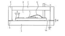
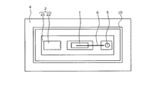
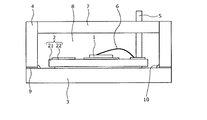
図1に示すように、パワー半導体モジュールは、パワー半導体チップ1と、積層基板2と、金属基板3と、端子ケース4と、金属端子5と、金属ワイヤ6と、蓋7と、封止材8と、中間層10と、を備える。
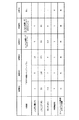
図7は、実施の形態にかかるパワー半導体モジュールの評価結果を示す表である。種々の条件で実施の形態にかかるパワー半導体モジュールを作成し、作成したパワー半導体モジュールに対して、ヒートショック試験を行った結果を示す。ヒートショック試験では、−40℃〜125℃の温度変化を1000回行った。
2 積層基板
21 絶縁性基板
22 導電性板
3 金属基板
4 端子ケース
5 金属端子
6 金属ワイヤ
7 蓋
8 封止材
9 接着剤
10 中間層
Claims (9)
- 半導体素子を搭載した積層基板と、
前記積層基板を搭載した金属基板と、
前記金属基板を接着剤で接着した樹脂ケースと、
前記樹脂ケース内を充填した封止材と、
前記金属基板と前記樹脂ケースとの接着部分と、前記封止材との間に設けられた中間層と、
を備え、
前記中間層は、線膨張係数が前記封止材の線膨張係数より大きく、前記接着剤の線膨張係数より小さいことを特徴とする半導体装置。 - 前記中間層は、線膨張係数が前記封止材の線膨張係数と、前記接着剤の線膨張係数との中間の値であることを特徴とする請求項1に記載の半導体装置。
- 前記中間層は、弾性率が前記封止材の弾性率より小さく、前記接着剤の弾性率より大きいことを特徴とする請求項1または2に記載の半導体装置。
- 前記中間層は、弾性率が前記封止材の弾性率と、前記接着剤の弾性率との中間の値であることを特徴とする請求項1または2に記載の半導体装置。
- 前記中間層は、熱硬化性樹脂に線膨張係数が20×10-6/K〜400×10-6/Kの添加粒子を配合したものであることを特徴とする請求項1〜4のいずれか一つに記載の半導体装置。
- 前記熱硬化性樹脂は、エポキシ樹脂、フェノール樹脂、またはマレイミド樹脂であり、前記添加粒子はシリコーンゴム、ブタジエンゴム、またはアクリロニトリルブタジエンゴムであることを特徴とする請求項5に記載の半導体装置。
- 前記添加粒子は、前記熱硬化性樹脂100質量部に対して1〜10質量部含まれることを特徴とする請求項5または6に記載の半導体装置。
- 前記封止材としての熱硬化性樹脂は、エポキシ樹脂、フェノール樹脂、またはマレイミド樹脂であり、前記接着剤の材料はシリコーンゴム、ブタジエンゴム、またはアクリロニトリルブタジエンゴムであることを特徴とする請求項5または6に記載の半導体装置。
- 半導体素子を積層基板に搭載する第1工程と、
前記積層基板を金属基板に搭載する第2工程と、
前記金属基板を接着剤で樹脂ケースに接着する第3工程と、
前記金属基板と前記樹脂ケースとの接着部分で前記樹脂ケースの内側に中間層を形成する第4工程と、
前記樹脂ケース内を封止材で充填する第5工程と、
を含み、
前記第4工程では、前記中間層を、線膨張係数が前記封止材の線膨張係数より大きく、前記接着剤の線膨張係数より小さく、前記接着部分と前記封止材との間に形成することを特徴とする半導体装置の製造方法。
Priority Applications (1)
| Application Number | Priority Date | Filing Date | Title |
|---|---|---|---|
| JP2017098915A JP6907697B2 (ja) | 2017-05-18 | 2017-05-18 | 半導体装置および半導体装置の製造方法 |
Applications Claiming Priority (1)
| Application Number | Priority Date | Filing Date | Title |
|---|---|---|---|
| JP2017098915A JP6907697B2 (ja) | 2017-05-18 | 2017-05-18 | 半導体装置および半導体装置の製造方法 |
Publications (2)
| Publication Number | Publication Date |
|---|---|
| JP2018195726A JP2018195726A (ja) | 2018-12-06 |
| JP6907697B2 true JP6907697B2 (ja) | 2021-07-21 |
Family
ID=64570655
Family Applications (1)
| Application Number | Title | Priority Date | Filing Date |
|---|---|---|---|
| JP2017098915A Active JP6907697B2 (ja) | 2017-05-18 | 2017-05-18 | 半導体装置および半導体装置の製造方法 |
Country Status (1)
| Country | Link |
|---|---|
| JP (1) | JP6907697B2 (ja) |
Families Citing this family (1)
| Publication number | Priority date | Publication date | Assignee | Title |
|---|---|---|---|---|
| JP2024132736A (ja) * | 2023-03-17 | 2024-10-01 | 株式会社東芝 | 半導体装置 |
Family Cites Families (5)
| Publication number | Priority date | Publication date | Assignee | Title |
|---|---|---|---|---|
| JP2913247B2 (ja) * | 1993-08-11 | 1999-06-28 | 株式会社日立製作所 | パワー半導体モジュール及び車両用インバータ装置 |
| JP4319591B2 (ja) * | 2004-07-15 | 2009-08-26 | 株式会社日立製作所 | 半導体パワーモジュール |
| JP6094413B2 (ja) * | 2013-07-18 | 2017-03-15 | 三菱電機株式会社 | 半導体モジュール及びその製造方法 |
| JP6171844B2 (ja) * | 2013-10-28 | 2017-08-02 | 富士電機株式会社 | パワー半導体モジュール |
| JP6540326B2 (ja) * | 2015-07-24 | 2019-07-10 | 富士電機株式会社 | 半導体装置およびその製造方法 |
-
2017
- 2017-05-18 JP JP2017098915A patent/JP6907697B2/ja active Active
Also Published As
| Publication number | Publication date |
|---|---|
| JP2018195726A (ja) | 2018-12-06 |
Similar Documents
| Publication | Publication Date | Title |
|---|---|---|
| JP5602077B2 (ja) | 半導体装置 | |
| JP4319591B2 (ja) | 半導体パワーモジュール | |
| JP6057927B2 (ja) | 半導体装置 | |
| JP7454129B2 (ja) | 半導体装置 | |
| JP4030930B2 (ja) | 半導体パワーモジュール | |
| JP2011228336A (ja) | 半導体装置および半導体装置の製造方法 | |
| JP6057926B2 (ja) | 半導体装置 | |
| JP2009252838A (ja) | 半導体装置 | |
| JPH10242333A (ja) | 半導体装置及び半導体装置の製造方法 | |
| CN104810360A (zh) | 电源模块封装以及制造电源模块封装的方法 | |
| JP2009194327A (ja) | 電力用半導体装置 | |
| JP6829809B2 (ja) | 半導体装置 | |
| JP2013191690A (ja) | 半導体装置及びその製造方法 | |
| JP3702877B2 (ja) | 樹脂封止型半導体装置、これに用いるダイボンド材および封止材 | |
| CN103972182A (zh) | 半导体装置及其制造方法以及粘接面强度的评估方法 | |
| CN105144373A (zh) | 半导体装置 | |
| JP7644899B2 (ja) | 半導体装置 | |
| CN104798194B (zh) | 半导体器件 | |
| CN113451225A (zh) | 功率半导体模块 | |
| JP7301492B2 (ja) | 樹脂組成物の製造方法 | |
| JP6907697B2 (ja) | 半導体装置および半導体装置の製造方法 | |
| US12315771B2 (en) | Semiconductor module | |
| JP7647253B2 (ja) | 半導体モジュールおよび半導体モジュールの製造方法 | |
| CN202352648U (zh) | 功率模块 | |
| JP6916997B2 (ja) | 半導体装置 |
Legal Events
| Date | Code | Title | Description |
|---|---|---|---|
| A621 | Written request for application examination |
Free format text: JAPANESE INTERMEDIATE CODE: A621 Effective date: 20200413 |
|
| A977 | Report on retrieval |
Free format text: JAPANESE INTERMEDIATE CODE: A971007 Effective date: 20210212 |
|
| A131 | Notification of reasons for refusal |
Free format text: JAPANESE INTERMEDIATE CODE: A131 Effective date: 20210316 |
|
| A521 | Request for written amendment filed |
Free format text: JAPANESE INTERMEDIATE CODE: A523 Effective date: 20210428 |
|
| TRDD | Decision of grant or rejection written | ||
| A01 | Written decision to grant a patent or to grant a registration (utility model) |
Free format text: JAPANESE INTERMEDIATE CODE: A01 Effective date: 20210601 |
|
| A61 | First payment of annual fees (during grant procedure) |
Free format text: JAPANESE INTERMEDIATE CODE: A61 Effective date: 20210614 |
|
| R150 | Certificate of patent or registration of utility model |
Ref document number: 6907697 Country of ref document: JP Free format text: JAPANESE INTERMEDIATE CODE: R150 |
|
| R250 | Receipt of annual fees |
Free format text: JAPANESE INTERMEDIATE CODE: R250 |
|
| R250 | Receipt of annual fees |
Free format text: JAPANESE INTERMEDIATE CODE: R250 |