JP6916397B2 - マルチビームレーザーデボンディング装置 - Google Patents
マルチビームレーザーデボンディング装置 Download PDFInfo
- Publication number
- JP6916397B2 JP6916397B2 JP2020558606A JP2020558606A JP6916397B2 JP 6916397 B2 JP6916397 B2 JP 6916397B2 JP 2020558606 A JP2020558606 A JP 2020558606A JP 2020558606 A JP2020558606 A JP 2020558606A JP 6916397 B2 JP6916397 B2 JP 6916397B2
- Authority
- JP
- Japan
- Prior art keywords
- laser
- laser beam
- electronic component
- debonding
- temperature
- Prior art date
- Legal status (The legal status is an assumption and is not a legal conclusion. Google has not performed a legal analysis and makes no representation as to the accuracy of the status listed.)
- Active
Links
Images





Classifications
-
- B—PERFORMING OPERATIONS; TRANSPORTING
- B23—MACHINE TOOLS; METAL-WORKING NOT OTHERWISE PROVIDED FOR
- B23K—SOLDERING OR UNSOLDERING; WELDING; CLADDING OR PLATING BY SOLDERING OR WELDING; CUTTING BY APPLYING HEAT LOCALLY, e.g. FLAME CUTTING; WORKING BY LASER BEAM
- B23K1/00—Soldering, e.g. brazing, or unsoldering
- B23K1/018—Unsoldering; Removal of melted solder or other residues
-
- B—PERFORMING OPERATIONS; TRANSPORTING
- B23—MACHINE TOOLS; METAL-WORKING NOT OTHERWISE PROVIDED FOR
- B23K—SOLDERING OR UNSOLDERING; WELDING; CLADDING OR PLATING BY SOLDERING OR WELDING; CUTTING BY APPLYING HEAT LOCALLY, e.g. FLAME CUTTING; WORKING BY LASER BEAM
- B23K26/00—Working by laser beam, e.g. welding, cutting or boring
- B23K26/02—Positioning or observing the workpiece, e.g. with respect to the point of impact; Aligning, aiming or focusing the laser beam
- B23K26/06—Shaping the laser beam, e.g. by masks or multi-focusing
- B23K26/067—Dividing the beam into multiple beams, e.g. multi-focusing
- B23K26/0676—Dividing the beam into multiple beams, e.g. multi-focusing into dependently operating sub-beams, e.g. an array of spots with fixed spatial relationship or for performing simultaneously identical operations
-
- H—ELECTRICITY
- H05—ELECTRIC TECHNIQUES NOT OTHERWISE PROVIDED FOR
- H05K—PRINTED CIRCUITS; CASINGS OR CONSTRUCTIONAL DETAILS OF ELECTRIC APPARATUS; MANUFACTURE OF ASSEMBLAGES OF ELECTRICAL COMPONENTS
- H05K13/00—Apparatus or processes specially adapted for manufacturing or adjusting assemblages of electric components
- H05K13/04—Mounting of components, e.g. of leadless components
- H05K13/0486—Replacement and removal of components
-
- B—PERFORMING OPERATIONS; TRANSPORTING
- B23—MACHINE TOOLS; METAL-WORKING NOT OTHERWISE PROVIDED FOR
- B23K—SOLDERING OR UNSOLDERING; WELDING; CLADDING OR PLATING BY SOLDERING OR WELDING; CUTTING BY APPLYING HEAT LOCALLY, e.g. FLAME CUTTING; WORKING BY LASER BEAM
- B23K26/00—Working by laser beam, e.g. welding, cutting or boring
- B23K26/02—Positioning or observing the workpiece, e.g. with respect to the point of impact; Aligning, aiming or focusing the laser beam
- B23K26/06—Shaping the laser beam, e.g. by masks or multi-focusing
- B23K26/0604—Shaping the laser beam, e.g. by masks or multi-focusing by a combination of beams
- B23K26/0608—Shaping the laser beam, e.g. by masks or multi-focusing by a combination of beams in the same heat affected zone [HAZ]
-
- B—PERFORMING OPERATIONS; TRANSPORTING
- B23—MACHINE TOOLS; METAL-WORKING NOT OTHERWISE PROVIDED FOR
- B23K—SOLDERING OR UNSOLDERING; WELDING; CLADDING OR PLATING BY SOLDERING OR WELDING; CUTTING BY APPLYING HEAT LOCALLY, e.g. FLAME CUTTING; WORKING BY LASER BEAM
- B23K1/00—Soldering, e.g. brazing, or unsoldering
- B23K1/0008—Soldering, e.g. brazing, or unsoldering specially adapted for particular articles or work
- B23K1/0016—Soldering of electronic components
-
- B—PERFORMING OPERATIONS; TRANSPORTING
- B23—MACHINE TOOLS; METAL-WORKING NOT OTHERWISE PROVIDED FOR
- B23K—SOLDERING OR UNSOLDERING; WELDING; CLADDING OR PLATING BY SOLDERING OR WELDING; CUTTING BY APPLYING HEAT LOCALLY, e.g. FLAME CUTTING; WORKING BY LASER BEAM
- B23K1/00—Soldering, e.g. brazing, or unsoldering
- B23K1/005—Soldering by means of radiant energy
- B23K1/0056—Soldering by means of radiant energy soldering by means of beams, e.g. lasers, electron beams [EB]
-
- B—PERFORMING OPERATIONS; TRANSPORTING
- B23—MACHINE TOOLS; METAL-WORKING NOT OTHERWISE PROVIDED FOR
- B23K—SOLDERING OR UNSOLDERING; WELDING; CLADDING OR PLATING BY SOLDERING OR WELDING; CUTTING BY APPLYING HEAT LOCALLY, e.g. FLAME CUTTING; WORKING BY LASER BEAM
- B23K26/00—Working by laser beam, e.g. welding, cutting or boring
- B23K26/02—Positioning or observing the workpiece, e.g. with respect to the point of impact; Aligning, aiming or focusing the laser beam
- B23K26/06—Shaping the laser beam, e.g. by masks or multi-focusing
- B23K26/073—Shaping the laser spot
-
- B—PERFORMING OPERATIONS; TRANSPORTING
- B23—MACHINE TOOLS; METAL-WORKING NOT OTHERWISE PROVIDED FOR
- B23K—SOLDERING OR UNSOLDERING; WELDING; CLADDING OR PLATING BY SOLDERING OR WELDING; CUTTING BY APPLYING HEAT LOCALLY, e.g. FLAME CUTTING; WORKING BY LASER BEAM
- B23K26/00—Working by laser beam, e.g. welding, cutting or boring
- B23K26/20—Bonding
-
- B—PERFORMING OPERATIONS; TRANSPORTING
- B23—MACHINE TOOLS; METAL-WORKING NOT OTHERWISE PROVIDED FOR
- B23K—SOLDERING OR UNSOLDERING; WELDING; CLADDING OR PLATING BY SOLDERING OR WELDING; CUTTING BY APPLYING HEAT LOCALLY, e.g. FLAME CUTTING; WORKING BY LASER BEAM
- B23K26/00—Working by laser beam, e.g. welding, cutting or boring
- B23K26/20—Bonding
- B23K26/32—Bonding taking account of the properties of the material involved
-
- B—PERFORMING OPERATIONS; TRANSPORTING
- B23—MACHINE TOOLS; METAL-WORKING NOT OTHERWISE PROVIDED FOR
- B23K—SOLDERING OR UNSOLDERING; WELDING; CLADDING OR PLATING BY SOLDERING OR WELDING; CUTTING BY APPLYING HEAT LOCALLY, e.g. FLAME CUTTING; WORKING BY LASER BEAM
- B23K26/00—Working by laser beam, e.g. welding, cutting or boring
- B23K26/352—Working by laser beam, e.g. welding, cutting or boring for surface treatment
- B23K26/354—Working by laser beam, e.g. welding, cutting or boring for surface treatment by melting
-
- B—PERFORMING OPERATIONS; TRANSPORTING
- B23—MACHINE TOOLS; METAL-WORKING NOT OTHERWISE PROVIDED FOR
- B23K—SOLDERING OR UNSOLDERING; WELDING; CLADDING OR PLATING BY SOLDERING OR WELDING; CUTTING BY APPLYING HEAT LOCALLY, e.g. FLAME CUTTING; WORKING BY LASER BEAM
- B23K26/00—Working by laser beam, e.g. welding, cutting or boring
- B23K26/60—Preliminary treatment
-
- H—ELECTRICITY
- H10—SEMICONDUCTOR DEVICES; ELECTRIC SOLID-STATE DEVICES NOT OTHERWISE PROVIDED FOR
- H10W—GENERIC PACKAGES, INTERCONNECTIONS, CONNECTORS OR OTHER CONSTRUCTIONAL DETAILS OF DEVICES COVERED BY CLASS H10
- H10W72/00—Interconnections or connectors in packages
- H10W72/071—Connecting or disconnecting
- H10W72/0711—Apparatus therefor
-
- B—PERFORMING OPERATIONS; TRANSPORTING
- B23—MACHINE TOOLS; METAL-WORKING NOT OTHERWISE PROVIDED FOR
- B23K—SOLDERING OR UNSOLDERING; WELDING; CLADDING OR PLATING BY SOLDERING OR WELDING; CUTTING BY APPLYING HEAT LOCALLY, e.g. FLAME CUTTING; WORKING BY LASER BEAM
- B23K2101/00—Articles made by soldering, welding or cutting
- B23K2101/36—Electric or electronic devices
- B23K2101/42—Printed circuits
-
- H—ELECTRICITY
- H10—SEMICONDUCTOR DEVICES; ELECTRIC SOLID-STATE DEVICES NOT OTHERWISE PROVIDED FOR
- H10W—GENERIC PACKAGES, INTERCONNECTIONS, CONNECTORS OR OTHER CONSTRUCTIONAL DETAILS OF DEVICES COVERED BY CLASS H10
- H10W72/00—Interconnections or connectors in packages
- H10W72/071—Connecting or disconnecting
-
- H—ELECTRICITY
- H10—SEMICONDUCTOR DEVICES; ELECTRIC SOLID-STATE DEVICES NOT OTHERWISE PROVIDED FOR
- H10W—GENERIC PACKAGES, INTERCONNECTIONS, CONNECTORS OR OTHER CONSTRUCTIONAL DETAILS OF DEVICES COVERED BY CLASS H10
- H10W72/00—Interconnections or connectors in packages
- H10W72/071—Connecting or disconnecting
- H10W72/0711—Apparatus therefor
- H10W72/07141—Means for applying energy, e.g. ovens or lasers
-
- H—ELECTRICITY
- H10—SEMICONDUCTOR DEVICES; ELECTRIC SOLID-STATE DEVICES NOT OTHERWISE PROVIDED FOR
- H10W—GENERIC PACKAGES, INTERCONNECTIONS, CONNECTORS OR OTHER CONSTRUCTIONAL DETAILS OF DEVICES COVERED BY CLASS H10
- H10W72/00—Interconnections or connectors in packages
- H10W72/071—Connecting or disconnecting
- H10W72/0711—Apparatus therefor
- H10W72/07183—Means for monitoring
-
- H—ELECTRICITY
- H10—SEMICONDUCTOR DEVICES; ELECTRIC SOLID-STATE DEVICES NOT OTHERWISE PROVIDED FOR
- H10W—GENERIC PACKAGES, INTERCONNECTIONS, CONNECTORS OR OTHER CONSTRUCTIONAL DETAILS OF DEVICES COVERED BY CLASS H10
- H10W72/00—Interconnections or connectors in packages
- H10W72/071—Connecting or disconnecting
- H10W72/072—Connecting or disconnecting of bump connectors
- H10W72/07231—Techniques
- H10W72/07235—Applying EM radiation, e.g. induction heating or using a laser
-
- H—ELECTRICITY
- H10—SEMICONDUCTOR DEVICES; ELECTRIC SOLID-STATE DEVICES NOT OTHERWISE PROVIDED FOR
- H10W—GENERIC PACKAGES, INTERCONNECTIONS, CONNECTORS OR OTHER CONSTRUCTIONAL DETAILS OF DEVICES COVERED BY CLASS H10
- H10W72/00—Interconnections or connectors in packages
- H10W72/071—Connecting or disconnecting
- H10W72/072—Connecting or disconnecting of bump connectors
- H10W72/07231—Techniques
- H10W72/07236—Soldering or alloying
-
- H—ELECTRICITY
- H10—SEMICONDUCTOR DEVICES; ELECTRIC SOLID-STATE DEVICES NOT OTHERWISE PROVIDED FOR
- H10W—GENERIC PACKAGES, INTERCONNECTIONS, CONNECTORS OR OTHER CONSTRUCTIONAL DETAILS OF DEVICES COVERED BY CLASS H10
- H10W72/00—Interconnections or connectors in packages
- H10W72/20—Bump connectors, e.g. solder bumps or copper pillars; Dummy bumps; Thermal bumps
- H10W72/251—Materials
- H10W72/252—Materials comprising solid metals or solid metalloids, e.g. PbSn, Ag or Cu
-
- H—ELECTRICITY
- H10—SEMICONDUCTOR DEVICES; ELECTRIC SOLID-STATE DEVICES NOT OTHERWISE PROVIDED FOR
- H10W—GENERIC PACKAGES, INTERCONNECTIONS, CONNECTORS OR OTHER CONSTRUCTIONAL DETAILS OF DEVICES COVERED BY CLASS H10
- H10W90/00—Package configurations
- H10W90/701—Package configurations characterised by the relative positions of pads or connectors relative to package parts
- H10W90/721—Package configurations characterised by the relative positions of pads or connectors relative to package parts of bump connectors
- H10W90/724—Package configurations characterised by the relative positions of pads or connectors relative to package parts of bump connectors between a chip and a stacked insulating package substrate, interposer or RDL
Landscapes
- Engineering & Computer Science (AREA)
- Physics & Mathematics (AREA)
- Optics & Photonics (AREA)
- Mechanical Engineering (AREA)
- Plasma & Fusion (AREA)
- Manufacturing & Machinery (AREA)
- Microelectronics & Electronic Packaging (AREA)
- Laser Beam Processing (AREA)
- Electric Connection Of Electric Components To Printed Circuits (AREA)
- Wire Bonding (AREA)
Description
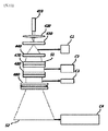
前記第一基板の領域より狭い領域の前記デボンディングの対象である電子部品の付着位置のみを含む第二基板領域に前記第一レーザービームと重ね合わせる第二レーザービームを照射して前記デボンディング対象の電子部品の半田を溶融が始まるデボンディング温度まで追加で加熱する第二レーザーモジュールを含む。
前記カメラ部からの出力信号に基づき前記レーザー照射部の各レーザーモジュールを独立的にコントロールするための制御信号を生成して、前記レーザー照射部に伝えるレーザー出力調整部をさらに含む。
320:第二レーザーモジュール
316、326:冷却装置
311,321:レーザー発振器
313、323:光学レンズモジュール
314、424:駆動装置
315、325:制御装置
317,327:電源供給部
Claims (6)
- 基板から電子部品をデボンディングするためのレーザーデボンディング装置において、デボンディング対象の電子部品と当該周辺電子部品の付着位置を含む所定範囲の第一基板領域に第一レーザービームを照射して前記電子部品の半田を所定の予熱温度まで加熱する一つ以上の第一レーザーモジュール、
前記第一基板領域より狭い領域である、前記デボンディング対象の電子部品の付着位置のみを含む第二基板領域に前記第一レーザービームより出力が低い第二レーザービームを前記第一レーザービームと互いに相違する最大出力と波長を有する状態で同時に重ね合わせるよう照射して前記デボンディング対象の電子部品の半田を溶融が始まるデボンディング温度まで追加で加熱する一つ以上の第二レーザーモジュール、
前記第一レーザービーム及び前記第二レーザービームによる前記電子部品のデボンディング過程を撮影するため、少なくとも一台のカメラモジュールで構成されるカメラ部、
前記第一レーザービーム及び前記第二レーザービームを放出するレーザー照射部、および、
前記カメラ部からの出力信号に基づき、前記第一レーザーモジュール及び前記第二レーザーモジュールからのレーザービームの形、重ね合わせ領域、照射角度、出力、波長、および温度を独立的にコントロールするための制御信号を生成して、前記レーザー照射部に伝えるレーザー出力調整部をさらに含み、
前記第一レーザービームと前記第二レーザービームの照射面は、前記第一レーザーモジュール及び前記第二レーザーモジュールに備えられたビームシェイパーによってそれぞれ四角形または円筒形で構成され、
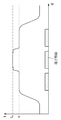
前記第一レーザーモジュールによる前記第一レーザービームの温度プロファイルは、半田の溶融点より低い所定の予熱温度までデボンディング対象の電子部品とその周辺の領域を含む所定の面積の第一基板領域の温度を上昇させ、前記第二レーザーモジュールによる前記第二レーザービームの温度プロファイルは、デボンディング対象の電子部品の付着領域である第二基板領域にのみデボンディング温度まで追加で上昇させてデボンディング対象の電子部品の付着領域内の電子部品の半田のみが溶融されるように誘導し、
前記第一レーザービームと前記第二レーザービームが照射されたとき、基板上の隣接領域に配置された前記周辺電子部品が過熱しないように、前記第一レーザービームと前記第二レーザービームの形状、重ね合わせ領域、エッジトリミング、照射角度、出力、波長、および温度を制御して目的の電子部品だけを選択的にデボンディングされる、
マルチビームレーザーデボンディング装置。 - 前記第一基板領域の前記予熱温度と前記第二基板領域の前記デボンディング温度の差は20℃から40℃である、
請求項1に記載のマルチビームレーザーデボンディング装置。 - 前記第一レーザーモジュール及び前記第二レーザーモジュールは、相互対称に配置され、前記第一レーザービーム及び前記第二レーザービームは同一のビームの照射角度を有し、互いに相違する最大出力と波長を有する、
請求項1に記載のマルチビームレーザーデボンディング装置。 - 前記第一基板領域の前記予熱温度と前記第二基板領域の前記デボンディング温度の偏差は10%から15%である、
請求項1に記載のマルチビームレーザーデボンディング装置。 - 前記第一レーザービームと前記第二レーザービームは、順次に照射される、
請求項1に記載のマルチビームレーザーデボンディング装置。 - 前記第一レーザービームと前記第二レーザービームの重ね合わせによる温度プロファイルは、2段階の上昇期と2段階の下降期を有する、
請求項1に記載のマルチビームレーザーデボンディング装置。
Applications Claiming Priority (3)
| Application Number | Priority Date | Filing Date | Title |
|---|---|---|---|
| KR10-2019-0013549 | 2019-02-01 | ||
| KR1020190013549A KR102174928B1 (ko) | 2019-02-01 | 2019-02-01 | 멀티 빔 레이저 디본딩 장치 및 방법 |
| PCT/KR2020/001598 WO2020159341A1 (ko) | 2019-02-01 | 2020-02-03 | 멀티 빔 레이저 디본딩 장치 및 방법 |
Publications (2)
| Publication Number | Publication Date |
|---|---|
| JP2021514854A JP2021514854A (ja) | 2021-06-17 |
| JP6916397B2 true JP6916397B2 (ja) | 2021-08-11 |
Family
ID=70429582
Family Applications (1)
| Application Number | Title | Priority Date | Filing Date |
|---|---|---|---|
| JP2020558606A Active JP6916397B2 (ja) | 2019-02-01 | 2020-02-03 | マルチビームレーザーデボンディング装置 |
Country Status (7)
| Country | Link |
|---|---|
| US (1) | US11699676B2 (ja) |
| EP (1) | EP3919218B1 (ja) |
| JP (1) | JP6916397B2 (ja) |
| KR (1) | KR102174928B1 (ja) |
| CN (2) | CN210470177U (ja) |
| TW (1) | TWI726600B (ja) |
| WO (1) | WO2020159341A1 (ja) |
Families Citing this family (8)
| Publication number | Priority date | Publication date | Assignee | Title |
|---|---|---|---|---|
| KR102174928B1 (ko) * | 2019-02-01 | 2020-11-05 | 레이저쎌 주식회사 | 멀티 빔 레이저 디본딩 장치 및 방법 |
| KR102901510B1 (ko) * | 2019-11-21 | 2025-12-17 | 레이저쎌 주식회사 | 레이저 리플로우 장치 및 레이저 리플로우 방법 |
| CN114038781B (zh) * | 2020-12-31 | 2025-09-09 | 广东聚华印刷显示技术有限公司 | 柔性器件的剥离方法 |
| CN114850667A (zh) * | 2021-02-05 | 2022-08-05 | 东莞市中麒光电技术有限公司 | 一种激光焊接方法及led显示模块 |
| WO2022254807A1 (ja) * | 2021-06-02 | 2022-12-08 | ソニーグループ株式会社 | レーザーはんだ装置、制御装置及びレーザーはんだ付け方法 |
| CN116038132A (zh) * | 2021-10-28 | 2023-05-02 | 广东汉邦激光科技有限公司 | 双激光打印装置、双激光打印方法及其制造的钽骨植入体 |
| CN117206616A (zh) * | 2022-06-02 | 2023-12-12 | 创新服务股份有限公司 | 电子元件的维修装置及维修方法 |
| CN115106652A (zh) * | 2022-07-13 | 2022-09-27 | 深圳市丰泰工业科技有限公司 | 一种基于激光的集成电路高速焊接方法及其装置 |
Family Cites Families (66)
| Publication number | Priority date | Publication date | Assignee | Title |
|---|---|---|---|---|
| JPS58159514A (ja) | 1982-03-18 | 1983-09-21 | Toshiba Corp | レ−ザビ−ム空間分布形成方法 |
| JPS60234768A (ja) * | 1984-05-08 | 1985-11-21 | Matsushita Electric Ind Co Ltd | レ−ザ−半田付装置 |
| US4877175A (en) * | 1988-12-30 | 1989-10-31 | General Electric Company | Laser debridging of microelectronic solder joints |
| JPH1041360A (ja) * | 1996-07-26 | 1998-02-13 | Haibetsuku:Kk | 被加熱対象物の選択的脱着方法 |
| KR100481994B1 (ko) * | 1996-08-27 | 2005-12-01 | 세이코 엡슨 가부시키가이샤 | 박리방법,박막디바이스의전사방법,및그것을이용하여제조되는박막디바이스,박막집적회로장치및액정표시장치 |
| WO1998057774A1 (de) * | 1997-06-13 | 1998-12-23 | Pac Tech - Packaging Technologies Gmbh | Verfahren und vorrichtung zur reparatur defekter lotverbindungsstellen |
| US7723642B2 (en) * | 1999-12-28 | 2010-05-25 | Gsi Group Corporation | Laser-based system for memory link processing with picosecond lasers |
| AU2001250208A1 (en) * | 2000-04-11 | 2001-10-23 | Gsi Lumonics Inc. | A method and system for laser drilling |
| DE50112936D1 (de) * | 2000-10-06 | 2007-10-11 | Pac Tech Gmbh | Vorrichtung zum entfernen von lotmaterial von einer lötstelle |
| WO2002028589A1 (de) * | 2000-10-06 | 2002-04-11 | Pac Tech - Packaging Technologies Gmbh | Verfahren und vorrichtung zur applikation von materialstücken auf ein werkstück |
| US7380697B2 (en) * | 2001-02-14 | 2008-06-03 | Honda Giken Kogyo Kabushiki Kaisha | Welding condition monitoring device |
| US6680213B2 (en) * | 2001-04-02 | 2004-01-20 | Micron Technology, Inc. | Method and system for fabricating contacts on semiconductor components |
| SG108262A1 (en) * | 2001-07-06 | 2005-01-28 | Inst Data Storage | Method and apparatus for cutting a multi-layer substrate by dual laser irradiation |
| TW554398B (en) * | 2001-08-10 | 2003-09-21 | Semiconductor Energy Lab | Method of peeling off and method of manufacturing semiconductor device |
| JP2003060340A (ja) * | 2001-08-17 | 2003-02-28 | Ricoh Co Ltd | はんだ偏析制御装置および部品リワーク方法 |
| US6750423B2 (en) * | 2001-10-25 | 2004-06-15 | Semiconductor Energy Laboratory Co., Ltd. | Laser irradiation method, laser irradiation apparatus, and method of manufacturing a semiconductor device |
| US7105048B2 (en) * | 2001-11-30 | 2006-09-12 | Semiconductor Energy Laboratory Co., Ltd. | Laser irradiation apparatus |
| TWI226139B (en) * | 2002-01-31 | 2005-01-01 | Osram Opto Semiconductors Gmbh | Method to manufacture a semiconductor-component |
| JP4693411B2 (ja) * | 2002-10-30 | 2011-06-01 | 株式会社半導体エネルギー研究所 | 半導体装置の作製方法 |
| JP4373115B2 (ja) * | 2003-04-04 | 2009-11-25 | 株式会社半導体エネルギー研究所 | 半導体装置の作製方法 |
| JP2004314165A (ja) * | 2003-04-21 | 2004-11-11 | Murata Mfg Co Ltd | レーザトリミング方法 |
| JP2005085708A (ja) * | 2003-09-10 | 2005-03-31 | Sony Corp | 局所加熱装置方法 |
| US8303738B2 (en) * | 2003-10-03 | 2012-11-06 | Sumitomo Electric Industries, Ltd. | Metal heating apparatus, metal heating method, and light source apparatus |
| CN101698254A (zh) * | 2003-10-03 | 2010-04-28 | 住友电气工业株式会社 | 金属加热装置及金属加热方法 |
| JP4175636B2 (ja) * | 2003-10-31 | 2008-11-05 | 株式会社日本製鋼所 | ガラスの切断方法 |
| WO2006104219A1 (en) * | 2005-03-29 | 2006-10-05 | Semiconductor Energy Laboratory Co., Ltd. | Laser irradiation apparatus and method for manufacturing semiconductor device |
| TWI275437B (en) * | 2005-06-30 | 2007-03-11 | Fujitsu Ltd | Method and device for removing micro component |
| US8087163B2 (en) * | 2005-11-18 | 2012-01-03 | PAC Tech—Packaging Technologies GmbH | Method of manufacturing a contact arrangement between a microelectronic component and a carrier |
| JP5110830B2 (ja) * | 2006-08-31 | 2012-12-26 | 株式会社半導体エネルギー研究所 | 半導体装置の作製方法 |
| US7732351B2 (en) * | 2006-09-21 | 2010-06-08 | Semiconductor Energy Laboratory Co., Ltd. | Manufacturing method of semiconductor device and laser processing apparatus |
| DE102007033074A1 (de) * | 2007-07-13 | 2009-01-15 | Pac Tech-Packaging Technologies Gmbh | Verfahren und Vorrichtung zur Entfernung von Lotmaterialdepots von einem Substrat |
| NL2001958C (en) * | 2008-09-05 | 2010-03-15 | Stichting Energie | Method of monolithic photo-voltaic module assembly. |
| US20100084744A1 (en) * | 2008-10-06 | 2010-04-08 | Zafiropoulo Arthur W | Thermal processing of substrates with pre- and post-spike temperature control |
| KR101770836B1 (ko) * | 2009-08-11 | 2017-08-23 | 하마마츠 포토닉스 가부시키가이샤 | 레이저 가공장치 및 레이저 가공방법 |
| US8986497B2 (en) * | 2009-12-07 | 2015-03-24 | Ipg Photonics Corporation | Laser lift off systems and methods |
| JP2011211073A (ja) * | 2010-03-30 | 2011-10-20 | Fujitsu Ltd | 電子部品のリペア装置、リペア方法、およびリペア用伝熱キャップ部材 |
| US20110287607A1 (en) * | 2010-04-02 | 2011-11-24 | Electro Scientific Industries, Inc. | Method and apparatus for improved wafer singulation |
| JP5802106B2 (ja) * | 2010-11-15 | 2015-10-28 | 東京応化工業株式会社 | 積層体、および分離方法 |
| US9895767B2 (en) * | 2011-05-10 | 2018-02-20 | The United States Of America, As Represented By The Secretary Of The Navy | Laser induced extra-planar elicitation |
| US9302348B2 (en) * | 2011-06-07 | 2016-04-05 | Ultratech Inc. | Ultrafast laser annealing with reduced pattern density effects in integrated circuit fabrication |
| KR101933549B1 (ko) * | 2011-07-06 | 2018-12-28 | 삼성전자주식회사 | 레이저를 이용한 반도체 칩의 제거장치 및 그의 제거방법 |
| JP2013066922A (ja) * | 2011-09-26 | 2013-04-18 | Toshiba Corp | 部材分離装置及び部材分離方法 |
| US8629043B2 (en) * | 2011-11-16 | 2014-01-14 | Taiwan Semiconductor Manufacturing Company, Ltd. | Methods for de-bonding carriers |
| JP5780938B2 (ja) * | 2011-12-13 | 2015-09-16 | 株式会社東芝 | 半導体装置の製造方法 |
| US20140144593A1 (en) * | 2012-11-28 | 2014-05-29 | International Business Machiness Corporation | Wafer debonding using long-wavelength infrared radiation ablation |
| US9586291B2 (en) * | 2012-11-28 | 2017-03-07 | Globalfoundries Inc | Adhesives for bonding handler wafers to device wafers and enabling mid-wavelength infrared laser ablation release |
| JP6110136B2 (ja) * | 2012-12-28 | 2017-04-05 | 株式会社ディスコ | ウエーハのレーザー加工方法およびレーザー加工装置 |
| US10226837B2 (en) * | 2013-03-15 | 2019-03-12 | Nlight, Inc. | Thermal processing with line beams |
| TWI610374B (zh) * | 2013-08-01 | 2018-01-01 | 格芯公司 | 用於將搬運器晶圓接合至元件晶圓以及能以中段波長紅外光雷射燒蝕釋出之接著劑 |
| KR102334815B1 (ko) * | 2014-02-19 | 2021-12-02 | 가부시키가이샤 한도오따이 에네루기 켄큐쇼 | 발광 장치 및 박리 방법 |
| JP2015188939A (ja) * | 2014-03-31 | 2015-11-02 | アイシン精機株式会社 | レーザ接合方法、レーザ接合品及びレーザ接合装置 |
| US20160133486A1 (en) * | 2014-11-07 | 2016-05-12 | International Business Machines Corporation | Double Layer Release Temporary Bond and Debond Processes and Systems |
| US9576836B2 (en) * | 2014-11-07 | 2017-02-21 | International Business Machines Corporation | Damage-free self-limiting through-substrate laser ablation |
| KR20170125384A (ko) * | 2015-03-10 | 2017-11-14 | 샤프 가부시키가이샤 | 박막 소자 장치의 제조 방법 및 그것에 사용하는 광조사 장치 |
| JP6488921B2 (ja) * | 2015-07-02 | 2019-03-27 | 富士通株式会社 | リワーク装置及びリワーク方法 |
| US10279576B2 (en) * | 2016-04-26 | 2019-05-07 | Semiconductor Energy Laboratory Co., Ltd. | Peeling method and manufacturing method of flexible device |
| TWI677393B (zh) * | 2017-05-10 | 2019-11-21 | 崔秉燦 | 夾具組件、包括此夾具組件的雷射加工方法及雷射加工裝置 |
| CN107414289B (zh) * | 2017-07-27 | 2019-05-17 | 京东方科技集团股份有限公司 | 一种激光剥离方法及激光剥离系统 |
| WO2019030819A1 (ja) * | 2017-08-08 | 2019-02-14 | シャープ株式会社 | Elデバイスの製造方法 |
| US10160053B1 (en) * | 2017-09-23 | 2018-12-25 | John Jerome Kusnierek | Cold gas blast jet for micro-electronic solder repair |
| JP6595558B2 (ja) * | 2017-10-30 | 2019-10-23 | ファナック株式会社 | レーザ加工システム |
| CN108400088B (zh) * | 2018-03-05 | 2021-07-20 | 大族激光科技产业集团股份有限公司 | 晶片结合及剥离的方法 |
| KR102120722B1 (ko) * | 2018-09-18 | 2020-06-09 | 레이저쎌 주식회사 | 마이크론급의 두께를 갖는 전자부품에 대한 레이저 리플로우 장치 |
| KR102174928B1 (ko) * | 2019-02-01 | 2020-11-05 | 레이저쎌 주식회사 | 멀티 빔 레이저 디본딩 장치 및 방법 |
| US20210005520A1 (en) * | 2019-07-02 | 2021-01-07 | Sharp Kabushiki Kaisha | Method and apparatus for manufacturing array device |
| US11247285B1 (en) * | 2020-04-03 | 2022-02-15 | Seagate Technology Llc | Fluidization of agglomerated solder microspheres |
-
2019
- 2019-02-01 KR KR1020190013549A patent/KR102174928B1/ko active Active
- 2019-04-04 CN CN201920452972.2U patent/CN210470177U/zh active Active
- 2019-04-04 CN CN201910271405.1A patent/CN111542216B/zh active Active
- 2019-10-09 US US16/596,925 patent/US11699676B2/en active Active
-
2020
- 2020-02-03 TW TW109103277A patent/TWI726600B/zh active
- 2020-02-03 JP JP2020558606A patent/JP6916397B2/ja active Active
- 2020-02-03 EP EP20749723.1A patent/EP3919218B1/en active Active
- 2020-02-03 WO PCT/KR2020/001598 patent/WO2020159341A1/ko not_active Ceased
Also Published As
| Publication number | Publication date |
|---|---|
| TW202030039A (zh) | 2020-08-16 |
| JP2021514854A (ja) | 2021-06-17 |
| KR102174928B1 (ko) | 2020-11-05 |
| CN111542216B (zh) | 2021-05-25 |
| EP3919218A1 (en) | 2021-12-08 |
| WO2020159341A1 (ko) | 2020-08-06 |
| US20200251442A1 (en) | 2020-08-06 |
| CN111542216A (zh) | 2020-08-14 |
| EP3919218B1 (en) | 2023-12-13 |
| US11699676B2 (en) | 2023-07-11 |
| KR20200095770A (ko) | 2020-08-11 |
| CN210470177U (zh) | 2020-05-05 |
| TWI726600B (zh) | 2021-05-01 |
| EP3919218A4 (en) | 2022-05-11 |
| EP3919218C0 (en) | 2023-12-13 |
Similar Documents
| Publication | Publication Date | Title |
|---|---|---|
| JP6916397B2 (ja) | マルチビームレーザーデボンディング装置 | |
| JP6608559B1 (ja) | ミクロンレベルの厚さを有する電子部品のレーザーリフロー装置 | |
| TWI403379B (zh) | 以短脈衝,固態紫外線雷射做微加工 | |
| KR20210082350A (ko) | 레이저 리플로 장치, 및, 레이저 리플로 방법 | |
| KR102376989B1 (ko) | 선형 이송 방식의 레이저 리플로우 장치 | |
| KR20200110028A (ko) | 멀티 빔 레이저 디본딩 장치 | |
| KR102228434B1 (ko) | 레이저 리플로우 장치의 레이저 리플로우 방법 | |
| KR20080101329A (ko) | 반도체칩 접합장치 | |
| KR102174929B1 (ko) | 레이저 리플로우 장치의 레이저 리플로우 방법 | |
| KR102174930B1 (ko) | 레이저 리플로우 장치의 레이저 가압 헤드 모듈 | |
| KR20210149980A (ko) | 솔더 에폭시를 이용한 레이저 본딩 및 디본딩하는 방법 | |
| KR20210099782A (ko) | 레이저 디본딩 장치 | |
| KR20210144282A (ko) | 선형 이송 방식의 레이저 리플로우 방법 | |
| JP7833902B2 (ja) | レーザーリフロー方法 | |
| KR20200145187A (ko) | 레이저 디본딩 장치의 레이저모듈 | |
| KR20210029344A (ko) | 레이저스캐너를 포함한 레이저 리플로우 장치 | |
| KR20200125205A (ko) | 레이저 디본딩 장치의 히팅모듈 | |
| KR20210090430A (ko) | 리플로우 장치의 가변 빔쉐이핑 옵틱 모듈 | |
| TWM673812U (zh) | 基板及半導體封裝 |
Legal Events
| Date | Code | Title | Description |
|---|---|---|---|
| A621 | Written request for application examination |
Free format text: JAPANESE INTERMEDIATE CODE: A621 Effective date: 20201021 |
|
| A871 | Explanation of circumstances concerning accelerated examination |
Free format text: JAPANESE INTERMEDIATE CODE: A871 Effective date: 20201021 |
|
| A975 | Report on accelerated examination |
Free format text: JAPANESE INTERMEDIATE CODE: A971005 Effective date: 20210402 |
|
| A131 | Notification of reasons for refusal |
Free format text: JAPANESE INTERMEDIATE CODE: A131 Effective date: 20210406 |
|
| A521 | Request for written amendment filed |
Free format text: JAPANESE INTERMEDIATE CODE: A523 Effective date: 20210629 |
|
| TRDD | Decision of grant or rejection written | ||
| A01 | Written decision to grant a patent or to grant a registration (utility model) |
Free format text: JAPANESE INTERMEDIATE CODE: A01 Effective date: 20210713 |
|
| A61 | First payment of annual fees (during grant procedure) |
Free format text: JAPANESE INTERMEDIATE CODE: A61 Effective date: 20210715 |
|
| R150 | Certificate of patent or registration of utility model |
Ref document number: 6916397 Country of ref document: JP Free format text: JAPANESE INTERMEDIATE CODE: R150 |
|
| R250 | Receipt of annual fees |
Free format text: JAPANESE INTERMEDIATE CODE: R250 |
|
| R250 | Receipt of annual fees |
Free format text: JAPANESE INTERMEDIATE CODE: R250 |