JP6971561B2 - 光電変換素子、撮像素子および撮像装置 - Google Patents
光電変換素子、撮像素子および撮像装置 Download PDFInfo
- Publication number
- JP6971561B2 JP6971561B2 JP2016220715A JP2016220715A JP6971561B2 JP 6971561 B2 JP6971561 B2 JP 6971561B2 JP 2016220715 A JP2016220715 A JP 2016220715A JP 2016220715 A JP2016220715 A JP 2016220715A JP 6971561 B2 JP6971561 B2 JP 6971561B2
- Authority
- JP
- Japan
- Prior art keywords
- photoelectric conversion
- organic compound
- conversion element
- image pickup
- layer
- Prior art date
- Legal status (The legal status is an assumption and is not a legal conclusion. Google has not performed a legal analysis and makes no representation as to the accuracy of the status listed.)
- Active
Links
Images




Classifications
-
- H—ELECTRICITY
- H10—SEMICONDUCTOR DEVICES; ELECTRIC SOLID-STATE DEVICES NOT OTHERWISE PROVIDED FOR
- H10K—ORGANIC ELECTRIC SOLID-STATE DEVICES
- H10K85/00—Organic materials used in the body or electrodes of devices covered by this subclass
- H10K85/20—Carbon compounds, e.g. carbon nanotubes or fullerenes
- H10K85/211—Fullerenes, e.g. C60
-
- H—ELECTRICITY
- H04—ELECTRIC COMMUNICATION TECHNIQUE
- H04N—PICTORIAL COMMUNICATION, e.g. TELEVISION
- H04N25/00—Circuitry of solid-state image sensors [SSIS]; Control thereof
- H04N25/70—SSIS architectures; Circuits associated therewith
- H04N25/76—Addressed sensors, e.g. MOS or CMOS sensors
- H04N25/78—Readout circuits for addressed sensors, e.g. output amplifiers or A/D converters
-
- H—ELECTRICITY
- H04—ELECTRIC COMMUNICATION TECHNIQUE
- H04N—PICTORIAL COMMUNICATION, e.g. TELEVISION
- H04N5/00—Details of television systems
- H04N5/38—Transmitter circuitry for the transmission of television signals according to analogue transmission standards
-
- H—ELECTRICITY
- H10—SEMICONDUCTOR DEVICES; ELECTRIC SOLID-STATE DEVICES NOT OTHERWISE PROVIDED FOR
- H10K—ORGANIC ELECTRIC SOLID-STATE DEVICES
- H10K30/00—Organic devices sensitive to infrared radiation, light, electromagnetic radiation of shorter wavelength or corpuscular radiation
-
- H—ELECTRICITY
- H10—SEMICONDUCTOR DEVICES; ELECTRIC SOLID-STATE DEVICES NOT OTHERWISE PROVIDED FOR
- H10K—ORGANIC ELECTRIC SOLID-STATE DEVICES
- H10K30/00—Organic devices sensitive to infrared radiation, light, electromagnetic radiation of shorter wavelength or corpuscular radiation
- H10K30/30—Organic devices sensitive to infrared radiation, light, electromagnetic radiation of shorter wavelength or corpuscular radiation comprising bulk heterojunctions, e.g. interpenetrating networks of donor and acceptor material domains
-
- H—ELECTRICITY
- H10—SEMICONDUCTOR DEVICES; ELECTRIC SOLID-STATE DEVICES NOT OTHERWISE PROVIDED FOR
- H10K—ORGANIC ELECTRIC SOLID-STATE DEVICES
- H10K39/00—Integrated devices, or assemblies of multiple devices, comprising at least one organic radiation-sensitive element covered by group H10K30/00
- H10K39/30—Devices controlled by radiation
- H10K39/32—Organic image sensors
-
- H—ELECTRICITY
- H10—SEMICONDUCTOR DEVICES; ELECTRIC SOLID-STATE DEVICES NOT OTHERWISE PROVIDED FOR
- H10K—ORGANIC ELECTRIC SOLID-STATE DEVICES
- H10K85/00—Organic materials used in the body or electrodes of devices covered by this subclass
- H10K85/30—Coordination compounds
- H10K85/341—Transition metal complexes, e.g. Ru(II)polypyridine complexes
- H10K85/342—Transition metal complexes, e.g. Ru(II)polypyridine complexes comprising iridium
-
- H—ELECTRICITY
- H10—SEMICONDUCTOR DEVICES; ELECTRIC SOLID-STATE DEVICES NOT OTHERWISE PROVIDED FOR
- H10K—ORGANIC ELECTRIC SOLID-STATE DEVICES
- H10K85/00—Organic materials used in the body or electrodes of devices covered by this subclass
- H10K85/60—Organic compounds having low molecular weight
- H10K85/615—Polycyclic condensed aromatic hydrocarbons, e.g. anthracene
- H10K85/622—Polycyclic condensed aromatic hydrocarbons, e.g. anthracene containing four rings, e.g. pyrene
-
- H—ELECTRICITY
- H10—SEMICONDUCTOR DEVICES; ELECTRIC SOLID-STATE DEVICES NOT OTHERWISE PROVIDED FOR
- H10K—ORGANIC ELECTRIC SOLID-STATE DEVICES
- H10K85/00—Organic materials used in the body or electrodes of devices covered by this subclass
- H10K85/60—Organic compounds having low molecular weight
- H10K85/615—Polycyclic condensed aromatic hydrocarbons, e.g. anthracene
- H10K85/625—Polycyclic condensed aromatic hydrocarbons, e.g. anthracene containing at least one aromatic ring having 7 or more carbon atoms, e.g. azulene
-
- H—ELECTRICITY
- H10—SEMICONDUCTOR DEVICES; ELECTRIC SOLID-STATE DEVICES NOT OTHERWISE PROVIDED FOR
- H10K—ORGANIC ELECTRIC SOLID-STATE DEVICES
- H10K85/00—Organic materials used in the body or electrodes of devices covered by this subclass
- H10K85/60—Organic compounds having low molecular weight
- H10K85/631—Amine compounds having at least two aryl rest on at least one amine-nitrogen atom, e.g. triphenylamine
-
- H—ELECTRICITY
- H10—SEMICONDUCTOR DEVICES; ELECTRIC SOLID-STATE DEVICES NOT OTHERWISE PROVIDED FOR
- H10K—ORGANIC ELECTRIC SOLID-STATE DEVICES
- H10K85/00—Organic materials used in the body or electrodes of devices covered by this subclass
- H10K85/60—Organic compounds having low molecular weight
- H10K85/649—Aromatic compounds comprising a hetero atom
- H10K85/655—Aromatic compounds comprising a hetero atom comprising only sulfur as heteroatom
-
- H—ELECTRICITY
- H10—SEMICONDUCTOR DEVICES; ELECTRIC SOLID-STATE DEVICES NOT OTHERWISE PROVIDED FOR
- H10K—ORGANIC ELECTRIC SOLID-STATE DEVICES
- H10K85/00—Organic materials used in the body or electrodes of devices covered by this subclass
- H10K85/60—Organic compounds having low molecular weight
- H10K85/649—Aromatic compounds comprising a hetero atom
- H10K85/656—Aromatic compounds comprising a hetero atom comprising two or more different heteroatoms per ring
-
- H—ELECTRICITY
- H10—SEMICONDUCTOR DEVICES; ELECTRIC SOLID-STATE DEVICES NOT OTHERWISE PROVIDED FOR
- H10K—ORGANIC ELECTRIC SOLID-STATE DEVICES
- H10K85/00—Organic materials used in the body or electrodes of devices covered by this subclass
- H10K85/60—Organic compounds having low molecular weight
- H10K85/649—Aromatic compounds comprising a hetero atom
- H10K85/657—Polycyclic condensed heteroaromatic hydrocarbons
-
- H—ELECTRICITY
- H10—SEMICONDUCTOR DEVICES; ELECTRIC SOLID-STATE DEVICES NOT OTHERWISE PROVIDED FOR
- H10K—ORGANIC ELECTRIC SOLID-STATE DEVICES
- H10K2101/00—Properties of the organic materials covered by group H10K85/00
- H10K2101/30—Highest occupied molecular orbital [HOMO], lowest unoccupied molecular orbital [LUMO] or Fermi energy values
-
- H—ELECTRICITY
- H10—SEMICONDUCTOR DEVICES; ELECTRIC SOLID-STATE DEVICES NOT OTHERWISE PROVIDED FOR
- H10K—ORGANIC ELECTRIC SOLID-STATE DEVICES
- H10K30/00—Organic devices sensitive to infrared radiation, light, electromagnetic radiation of shorter wavelength or corpuscular radiation
- H10K30/20—Organic devices sensitive to infrared radiation, light, electromagnetic radiation of shorter wavelength or corpuscular radiation comprising organic-organic junctions, e.g. donor-acceptor junctions
- H10K30/211—Organic devices sensitive to infrared radiation, light, electromagnetic radiation of shorter wavelength or corpuscular radiation comprising organic-organic junctions, e.g. donor-acceptor junctions comprising multiple junctions, e.g. double heterojunctions
-
- H—ELECTRICITY
- H10—SEMICONDUCTOR DEVICES; ELECTRIC SOLID-STATE DEVICES NOT OTHERWISE PROVIDED FOR
- H10K—ORGANIC ELECTRIC SOLID-STATE DEVICES
- H10K30/00—Organic devices sensitive to infrared radiation, light, electromagnetic radiation of shorter wavelength or corpuscular radiation
- H10K30/30—Organic devices sensitive to infrared radiation, light, electromagnetic radiation of shorter wavelength or corpuscular radiation comprising bulk heterojunctions, e.g. interpenetrating networks of donor and acceptor material domains
- H10K30/353—Organic devices sensitive to infrared radiation, light, electromagnetic radiation of shorter wavelength or corpuscular radiation comprising bulk heterojunctions, e.g. interpenetrating networks of donor and acceptor material domains comprising blocking layers, e.g. exciton blocking layers
-
- H—ELECTRICITY
- H10—SEMICONDUCTOR DEVICES; ELECTRIC SOLID-STATE DEVICES NOT OTHERWISE PROVIDED FOR
- H10K—ORGANIC ELECTRIC SOLID-STATE DEVICES
- H10K85/00—Organic materials used in the body or electrodes of devices covered by this subclass
- H10K85/60—Organic compounds having low molecular weight
- H10K85/615—Polycyclic condensed aromatic hydrocarbons, e.g. anthracene
- H10K85/626—Polycyclic condensed aromatic hydrocarbons, e.g. anthracene containing more than one polycyclic condensed aromatic rings, e.g. bis-anthracene
-
- H—ELECTRICITY
- H10—SEMICONDUCTOR DEVICES; ELECTRIC SOLID-STATE DEVICES NOT OTHERWISE PROVIDED FOR
- H10K—ORGANIC ELECTRIC SOLID-STATE DEVICES
- H10K85/00—Organic materials used in the body or electrodes of devices covered by this subclass
- H10K85/60—Organic compounds having low molecular weight
- H10K85/631—Amine compounds having at least two aryl rest on at least one amine-nitrogen atom, e.g. triphenylamine
- H10K85/636—Amine compounds having at least two aryl rest on at least one amine-nitrogen atom, e.g. triphenylamine comprising heteroaromatic hydrocarbons as substituents on the nitrogen atom
-
- Y—GENERAL TAGGING OF NEW TECHNOLOGICAL DEVELOPMENTS; GENERAL TAGGING OF CROSS-SECTIONAL TECHNOLOGIES SPANNING OVER SEVERAL SECTIONS OF THE IPC; TECHNICAL SUBJECTS COVERED BY FORMER USPC CROSS-REFERENCE ART COLLECTIONS [XRACs] AND DIGESTS
- Y02—TECHNOLOGIES OR APPLICATIONS FOR MITIGATION OR ADAPTATION AGAINST CLIMATE CHANGE
- Y02E—REDUCTION OF GREENHOUSE GAS [GHG] EMISSIONS, RELATED TO ENERGY GENERATION, TRANSMISSION OR DISTRIBUTION
- Y02E10/00—Energy generation through renewable energy sources
- Y02E10/50—Photovoltaic [PV] energy
- Y02E10/549—Organic PV cells
Landscapes
- Chemical & Material Sciences (AREA)
- Engineering & Computer Science (AREA)
- Materials Engineering (AREA)
- Physics & Mathematics (AREA)
- Spectroscopy & Molecular Physics (AREA)
- Signal Processing (AREA)
- Multimedia (AREA)
- Electromagnetism (AREA)
- Nanotechnology (AREA)
- Crystallography & Structural Chemistry (AREA)
- Inorganic Chemistry (AREA)
- Solid State Image Pick-Up Elements (AREA)
- Light Receiving Elements (AREA)
- Electroluminescent Light Sources (AREA)
- Transforming Light Signals Into Electric Signals (AREA)
Description
ΔE=第一の有機化合物の酸化電位−第二の有機化合物の還元電位 (A)
ΔE≧1.79 [V] (B)
本実施形態においては、アノードとカソードとの間に有機化合物からなる光電変換層を有する光電変換素子を例に挙げて説明する。
ΔEは下記式(A)にて定義されるエネルギーギャップである。
ΔE=第一の有機化合物の酸化電位−第二の有機化合物の還元電位 (A)
またΔEは、下記式(B)を満たす。
ΔE≧1.79 [V] (B)

本実施形態に係る撮像素子は、複数の画素を有し、画素は、本発明に係る光電変換素子と、光電変換素子に接続されている読み出しトランジスタを有する。
酸化電位などの電気化学特性の評価は、サリクリックボルタンメトリー(CV)によって行うことができる。
本実施例では、ΔE≧1.79Vとなる第一の有機化合物と第二の有機化合物との組み合わせを用いて光電変換素子を作製した。作製した光電変換素子を用いて暗電流を測定した。
B:100pA/cm2以上1000pA/cm2未満
C:1000pA/cm2以上
Aは良好、B及びCは不良とした。
第一の有機化合物及び第二の有機化合物の組み合わせを表4に示す組み合わせとする以外は、実施例1と同様に光電変換素子を作製した。実施例1乃至15についての結果を次の表4に示す。
第一の有機化合物と第二の有機化合物の組み合わせを表5の組み合わせとする以外は実施例1と同様に光電変換素子を作製した。表5の化合物の組み合わせは、ΔE<1.79Vの組み合わせである。作製した光電変換素子を実施例1と同様の測定法で暗電流評価を行った。
実施例1において作製した光電変換素子を用いて、暗電流の温度依存性を測定した。図6は、実施例1の光電変換素子のアレニウスプロットである。縦軸は、60℃における暗電流値で規格化した暗電流値である。縦軸の目盛は常用対数である。横軸は絶対温度の逆数である。図6において60℃付近から高温側に向かって傾きの絶対値が大きくなる。この傾きから次式(5)に従い活性化エネルギーを求めた。
例示化合物1−3、1−7、1−13、1−21、1−23を第一の有機化合物とした以外は実施例1と同様に光電変換素子を作製し、実施例16と同様に暗電流の活性化エネルギーを求めた。図7は活性化エネルギー(Ea)とΔEとの関係を示した図である。図7より、ΔEが1.79V以上となることで、活性化エネルギーが大きくなることがわかる。これは、ΔEが1.79V以上である場合、熱励起による電荷発生確率が低下することを指す。
封止層にCVD法による窒化珪素層を用いた以外は、実施例1と同様にして光電変換素子を作製した。窒化珪素層は1μmの層厚で形成した。この素子に365nmのLED光を1W/cm2の強度で24h照射して耐久性を評価した。
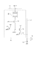
2 正孔ブロック層
3 電子ブロック層
4 アノード電極
5 カソード電極
6 読み出し回路
7 保護層
8 カラーフィルタ
9 マイクロレンズ
Claims (13)
- 下部電極、光電変換層、上部電極をこの順に有し、前記下部電極と前記上部電極との間に電圧を印加する光電変換素子であって、
前記光電変換層は、第一の有機化合物と、第二の有機化合物とを有し、
前記第一の有機化合物の酸化電位は、前記第二の有機化合物の酸化電位よりも小さく、
下記式(A)で表されるΔEが、下記式(B)を満たし、
前記第一の有機化合物が下記構造式で表されることを特徴とする光電変換素子。
ΔE=第一の有機化合物の酸化電位−第二の有機化合物の還元電位 (A)
ΔE≧1.79 [V] (B)
- 前記第一の有機化合物の酸化電位は0.96V以上であることを特徴とする請求項1に記載の光電変換素子。
- 前記第一の有機化合物の濃度は、前記第一の有機化合物と前記第二の有機化合物との合計を100重量%とした場合、35重量%未満であることを特徴とする請求項1または2に記載の光電変換素子。
- 前記第一の有機化合物が、硫黄原子を含む5員環を有する複素環基を含む有機化合物、フルオランテン骨格を有する有機化合物、金属錯体のいずれかであることを特徴とする請求項1乃至3のいずれか一項に記載の光電変換素子。
- 前記第一の有機化合物が、下記構造式で表されることを特徴とする請求項1乃至4のいずれか一項に記載の光電変換素子。
- 前記第二の有機化合物がフラーレン誘導体であることを特徴とする請求項1乃至5のいずれか一項に記載の光電変換素子。
- 前記フラーレン誘導体が、フラーレンC60であることを特徴とする請求項6に記載の光電変換素子。
- 前記上部電極の上に封止層を有することを特徴とする請求項1乃至7のいずれか一項に記載の光電変換素子。
- 複数の画素と、前記画素に接続されている信号処理回路とを有する撮像素子であって、
前記画素は、請求項1乃至8のいずれか一項に記載の光電変換素子と、前記光電変換素子に接続されている読み出し回路と、を有することを特徴とする撮像素子。 - 複数のレンズを有する光学部と、前記光学部を透過した光を受光する撮像素子とを有する撮像装置であって、
前記撮像素子は、請求項9に記載の撮像素子であることを特徴とする撮像装置。 - 外部からの信号を受信する受信部をさらに有することを特徴とする請求項10に記載の撮像装置。
- 前記信号は、撮像装置の撮像範囲、撮像の開始、撮像の終了の少なくともいずれかを制御する信号であることを特徴とする請求項11に記載の撮像装置。
- 外部に情報を送信する送信部をさらに有することを特徴とする請求項10乃至12のいずれか一項に記載の撮像装置。
Priority Applications (2)
| Application Number | Priority Date | Filing Date | Title |
|---|---|---|---|
| JP2016220715A JP6971561B2 (ja) | 2016-11-11 | 2016-11-11 | 光電変換素子、撮像素子および撮像装置 |
| US15/806,004 US10468614B2 (en) | 2016-11-11 | 2017-11-07 | Photoelectric conversion element, image pick-up element, and image pick-up apparatus |
Applications Claiming Priority (1)
| Application Number | Priority Date | Filing Date | Title |
|---|---|---|---|
| JP2016220715A JP6971561B2 (ja) | 2016-11-11 | 2016-11-11 | 光電変換素子、撮像素子および撮像装置 |
Publications (2)
| Publication Number | Publication Date |
|---|---|
| JP2018078241A JP2018078241A (ja) | 2018-05-17 |
| JP6971561B2 true JP6971561B2 (ja) | 2021-11-24 |
Family
ID=62108942
Family Applications (1)
| Application Number | Title | Priority Date | Filing Date |
|---|---|---|---|
| JP2016220715A Active JP6971561B2 (ja) | 2016-11-11 | 2016-11-11 | 光電変換素子、撮像素子および撮像装置 |
Country Status (2)
| Country | Link |
|---|---|
| US (1) | US10468614B2 (ja) |
| JP (1) | JP6971561B2 (ja) |
Families Citing this family (1)
| Publication number | Priority date | Publication date | Assignee | Title |
|---|---|---|---|---|
| TWI862629B (zh) * | 2019-07-30 | 2024-11-21 | 日商索尼股份有限公司 | 攝像元件及攝像裝置 |
Family Cites Families (7)
| Publication number | Priority date | Publication date | Assignee | Title |
|---|---|---|---|---|
| JP4677314B2 (ja) | 2005-09-20 | 2011-04-27 | 富士フイルム株式会社 | センサーおよび有機光電変換素子の駆動方法 |
| US20070272918A1 (en) * | 2006-05-25 | 2007-11-29 | Barry Rand | Organic photosensitive devices using subphthalocyanine compounds |
| JP4604128B2 (ja) | 2008-10-15 | 2010-12-22 | 富士フイルム株式会社 | 光電変換素子及び撮像素子 |
| JP2011199263A (ja) * | 2010-02-25 | 2011-10-06 | Fujifilm Corp | 光電変換素子、撮像素子、撮像素子の製造方法、撮像装置 |
| JP6158937B2 (ja) * | 2012-11-21 | 2017-07-05 | エルジー・ケム・リミテッド | フルオランテン化合物およびそれを含む有機電子素子 |
| EP2948463A2 (en) * | 2013-03-11 | 2015-12-02 | Saudi Basic Industries Corporation | Aryloxy-phthalocyanines of group iv metals |
| JP6500786B2 (ja) * | 2014-02-14 | 2019-04-17 | 東洋紡株式会社 | 有機半導体材料 |
-
2016
- 2016-11-11 JP JP2016220715A patent/JP6971561B2/ja active Active
-
2017
- 2017-11-07 US US15/806,004 patent/US10468614B2/en active Active
Also Published As
| Publication number | Publication date |
|---|---|
| US20180138432A1 (en) | 2018-05-17 |
| JP2018078241A (ja) | 2018-05-17 |
| US10468614B2 (en) | 2019-11-05 |
Similar Documents
| Publication | Publication Date | Title |
|---|---|---|
| Sutherland et al. | Sensitive, fast, and stable perovskite photodetectors exploiting interface engineering | |
| JP7102114B2 (ja) | 光電変換素子、撮像素子および撮像装置 | |
| CN110301052B (zh) | 光电转换元件、和使用其的光学区域传感器、图像拾取元件和图像拾取设备 | |
| JP6645700B2 (ja) | 有機光電変換素子、二次元センサ、画像センサ及び撮像装置 | |
| JP6833351B2 (ja) | 有機光電変換素子、光エリアセンサ、撮像素子および撮像装置 | |
| US12150320B2 (en) | Photoelectric conversion element, measuring method of the same, solid-state imaging device, electronic device, and solar cell | |
| JP2022021347A (ja) | 有機化合物及び有機光電変換素子 | |
| JP7013163B2 (ja) | 有機化合物及び光電変換素子 | |
| JP6932564B2 (ja) | 有機光電変換素子、撮像素子及び撮像装置 | |
| KR20120031922A (ko) | 광전 변환 소자, 고체 촬상 소자, 촬상 장치, 및 광전 변환 소자의 제조 방법 | |
| US20190267545A1 (en) | Photoelectric conversion element, and imaging element and imaging apparatus including the same | |
| WO2017138363A1 (ja) | 有機光電変換素子、光エリアセンサ、撮像素子及び撮像装置 | |
| JP2019099570A (ja) | フラーレン誘導体及びそれを含む薄膜、光電素子並びにイメージセンサ及び電子装置 | |
| WO2018147202A1 (ja) | 光電変換素子、及びこれを用いた光エリアセンサ、撮像素子、撮像装置 | |
| JP7039285B2 (ja) | 光電変換素子、及びこれを用いた光エリアセンサ、撮像素子、撮像装置 | |
| JP2015103598A (ja) | 有機機能層付き基板およびその製造方法 | |
| JP6971561B2 (ja) | 光電変換素子、撮像素子および撮像装置 | |
| WO2018088325A1 (ja) | 光電変換素子、撮像素子および撮像装置 | |
| JP2022054441A (ja) | シアニン化合物及び光電変換素子 | |
| JP2018078240A (ja) | 光電変換素子、それを有する撮像素子及び撮像装置 | |
| JP2019006718A (ja) | 有機化合物、それを有する有機電子デバイス、それを有する光電変換素子、撮像素子および撮像装置 |
Legal Events
| Date | Code | Title | Description |
|---|---|---|---|
| A621 | Written request for application examination |
Free format text: JAPANESE INTERMEDIATE CODE: A621 Effective date: 20191007 |
|
| A131 | Notification of reasons for refusal |
Free format text: JAPANESE INTERMEDIATE CODE: A131 Effective date: 20200825 |
|
| A977 | Report on retrieval |
Free format text: JAPANESE INTERMEDIATE CODE: A971007 Effective date: 20200826 |
|
| A521 | Request for written amendment filed |
Free format text: JAPANESE INTERMEDIATE CODE: A523 Effective date: 20201022 |
|
| A131 | Notification of reasons for refusal |
Free format text: JAPANESE INTERMEDIATE CODE: A131 Effective date: 20210406 |
|
| A521 | Request for written amendment filed |
Free format text: JAPANESE INTERMEDIATE CODE: A523 Effective date: 20210525 |
|
| TRDD | Decision of grant or rejection written | ||
| A01 | Written decision to grant a patent or to grant a registration (utility model) |
Free format text: JAPANESE INTERMEDIATE CODE: A01 Effective date: 20211005 |
|
| A61 | First payment of annual fees (during grant procedure) |
Free format text: JAPANESE INTERMEDIATE CODE: A61 Effective date: 20211102 |
|
| R151 | Written notification of patent or utility model registration |
Ref document number: 6971561 Country of ref document: JP Free format text: JAPANESE INTERMEDIATE CODE: R151 |