JP6977876B2 - パワーデバイス駆動装置及びその製造方法 - Google Patents
パワーデバイス駆動装置及びその製造方法 Download PDFInfo
- Publication number
- JP6977876B2 JP6977876B2 JP2020518859A JP2020518859A JP6977876B2 JP 6977876 B2 JP6977876 B2 JP 6977876B2 JP 2020518859 A JP2020518859 A JP 2020518859A JP 2020518859 A JP2020518859 A JP 2020518859A JP 6977876 B2 JP6977876 B2 JP 6977876B2
- Authority
- JP
- Japan
- Prior art keywords
- power supply
- control signal
- output voltage
- supply voltage
- power device
- Prior art date
- Legal status (The legal status is an assumption and is not a legal conclusion. Google has not performed a legal analysis and makes no representation as to the accuracy of the status listed.)
- Active
Links
Images




Classifications
-
- H—ELECTRICITY
- H02—GENERATION; CONVERSION OR DISTRIBUTION OF ELECTRIC POWER
- H02M—APPARATUS FOR CONVERSION BETWEEN AC AND AC, BETWEEN AC AND DC, OR BETWEEN DC AND DC, AND FOR USE WITH MAINS OR SIMILAR POWER SUPPLY SYSTEMS; CONVERSION OF DC OR AC INPUT POWER INTO SURGE OUTPUT POWER; CONTROL OR REGULATION THEREOF
- H02M3/00—Conversion of DC power input into DC power output
- H02M3/22—Conversion of DC power input into DC power output with intermediate conversion into AC
- H02M3/24—Conversion of DC power input into DC power output with intermediate conversion into AC by static converters
- H02M3/28—Conversion of DC power input into DC power output with intermediate conversion into AC by static converters using discharge tubes with control electrode or semiconductor devices with control electrode to produce the intermediate AC
- H02M3/325—Conversion of DC power input into DC power output with intermediate conversion into AC by static converters using discharge tubes with control electrode or semiconductor devices with control electrode to produce the intermediate AC using devices of a triode or a transistor type requiring continuous application of a control signal
- H02M3/335—Conversion of DC power input into DC power output with intermediate conversion into AC by static converters using discharge tubes with control electrode or semiconductor devices with control electrode to produce the intermediate AC using devices of a triode or a transistor type requiring continuous application of a control signal using semiconductor devices only
- H02M3/33507—Conversion of DC power input into DC power output with intermediate conversion into AC by static converters using discharge tubes with control electrode or semiconductor devices with control electrode to produce the intermediate AC using devices of a triode or a transistor type requiring continuous application of a control signal using semiconductor devices only with automatic control of the output voltage or current, e.g. flyback converters
- H02M3/33523—Conversion of DC power input into DC power output with intermediate conversion into AC by static converters using discharge tubes with control electrode or semiconductor devices with control electrode to produce the intermediate AC using devices of a triode or a transistor type requiring continuous application of a control signal using semiconductor devices only with automatic control of the output voltage or current, e.g. flyback converters with galvanic isolation between input and output of both the power stage and the feedback loop
-
- H—ELECTRICITY
- H02—GENERATION; CONVERSION OR DISTRIBUTION OF ELECTRIC POWER
- H02M—APPARATUS FOR CONVERSION BETWEEN AC AND AC, BETWEEN AC AND DC, OR BETWEEN DC AND DC, AND FOR USE WITH MAINS OR SIMILAR POWER SUPPLY SYSTEMS; CONVERSION OF DC OR AC INPUT POWER INTO SURGE OUTPUT POWER; CONTROL OR REGULATION THEREOF
- H02M1/00—Details of apparatus for conversion
- H02M1/08—Circuits specially adapted for the generation of control voltages for semiconductor devices incorporated in static converters
-
- H—ELECTRICITY
- H02—GENERATION; CONVERSION OR DISTRIBUTION OF ELECTRIC POWER
- H02M—APPARATUS FOR CONVERSION BETWEEN AC AND AC, BETWEEN AC AND DC, OR BETWEEN DC AND DC, AND FOR USE WITH MAINS OR SIMILAR POWER SUPPLY SYSTEMS; CONVERSION OF DC OR AC INPUT POWER INTO SURGE OUTPUT POWER; CONTROL OR REGULATION THEREOF
- H02M1/00—Details of apparatus for conversion
- H02M1/0003—Details of control, feedback or regulation circuits
- H02M1/0006—Arrangements for supplying an adequate voltage to the control circuit of converters
-
- H—ELECTRICITY
- H02—GENERATION; CONVERSION OR DISTRIBUTION OF ELECTRIC POWER
- H02M—APPARATUS FOR CONVERSION BETWEEN AC AND AC, BETWEEN AC AND DC, OR BETWEEN DC AND DC, AND FOR USE WITH MAINS OR SIMILAR POWER SUPPLY SYSTEMS; CONVERSION OF DC OR AC INPUT POWER INTO SURGE OUTPUT POWER; CONTROL OR REGULATION THEREOF
- H02M1/00—Details of apparatus for conversion
- H02M1/0003—Details of control, feedback or regulation circuits
- H02M1/0016—Control circuits providing compensation of output voltage deviations using feedforward of disturbance parameters
- H02M1/0022—Control circuits providing compensation of output voltage deviations using feedforward of disturbance parameters the disturbance parameters being input voltage fluctuations
Landscapes
- Engineering & Computer Science (AREA)
- Power Engineering (AREA)
- Dc-Dc Converters (AREA)
Description
図1は、実施の形態1に係るパワーデバイス駆動装置を示す回路図である。電源端子と接地端子の間にトランス1の1次側コイルとスイッチング素子2が直列に接続されている。コンデンサ3がトランス1の1次側コイルに並列に接続されている。
図4は、実施の形態2に係るパワーデバイス駆動装置を示す回路図である。実施の形態1では制御部4に電源電圧のみ入力していたが、本実施の形態ではパワーデバイス8の駆動負荷情報であるキャリア周波数も入力する。図5は、実施の形態2に係るテーブルを示す図である。テーブルは、所望の2次側出力電圧が得られるような電源電圧とパワーデバイスのキャリア周波数と制御信号のデューティ比をまとめたものである。制御部4は、図5のテーブルを参照して電源電圧とパワーデバイスのキャリア周波数に対応するディーティ比を持った制御信号を生成する。これにより出力負荷変動にも対応できる。その他の構成及び効果は実施の形態1と同様である。
Claims (4)
- 制御信号を生成する制御部と、
前記制御信号に応じてスイッチングして電源電圧から1次側入力電圧を生成するスイッチング素子と、
前記1次側入力電圧を2次側出力電圧に変換するトランスと、
前記2次側出力電圧に応じてパワーデバイスを駆動する駆動回路とを備え、
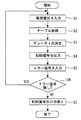
前記制御部は、所望の2次側出力電圧が得られるような電源電圧と制御信号の設定値の対応関係をまとめたテーブルを有し、前記テーブルを参照して前記電源電圧に対応する設定値を持った前記制御信号を生成し、
前記テーブルは、所望の2次側出力電圧が得られるような電源電圧とパワーデバイスのキャリア周波数と制御信号の設定値の対応関係をまとめたものであり、
前記制御部は、前記テーブルを参照して前記電源電圧と前記パワーデバイスのキャリア周波数に対応する設定値を持った前記制御信号を生成することを特徴とするパワーデバイス駆動装置。 - 前記制御部は前記2次側出力電圧をフィードバックすることなく前記制御信号を生成することを特徴とする請求項1に記載のパワーデバイス駆動装置。
- 前記制御信号はパルス幅変調信号であり、
前記テーブルは、所望の2次側出力電圧が得られるような電源電圧と制御信号のデューティ比の対応関係をまとめたものであることを特徴とする請求項1又は2に記載のパワーデバイス駆動装置。 - 請求項1〜3の何れか1項に記載のパワーデバイス駆動装置を製造する方法であって、
前記制御部に入力する前記電源電圧を変化させながら前記2次側出力電圧をモニタして前記2次側出力電圧が所望の電圧となるように前記テーブルを設定することを特徴とするパワーデバイス駆動装置の製造方法。
Applications Claiming Priority (1)
| Application Number | Priority Date | Filing Date | Title |
|---|---|---|---|
| PCT/JP2018/018787 WO2019220544A1 (ja) | 2018-05-15 | 2018-05-15 | パワーデバイス駆動装置及びその製造方法 |
Publications (2)
| Publication Number | Publication Date |
|---|---|
| JPWO2019220544A1 JPWO2019220544A1 (ja) | 2021-02-12 |
| JP6977876B2 true JP6977876B2 (ja) | 2021-12-08 |
Family
ID=68539689
Family Applications (1)
| Application Number | Title | Priority Date | Filing Date |
|---|---|---|---|
| JP2020518859A Active JP6977876B2 (ja) | 2018-05-15 | 2018-05-15 | パワーデバイス駆動装置及びその製造方法 |
Country Status (5)
| Country | Link |
|---|---|
| US (1) | US11563380B2 (ja) |
| JP (1) | JP6977876B2 (ja) |
| CN (1) | CN112088481B (ja) |
| DE (1) | DE112018007618T5 (ja) |
| WO (1) | WO2019220544A1 (ja) |
Family Cites Families (14)
| Publication number | Priority date | Publication date | Assignee | Title |
|---|---|---|---|---|
| JP3688448B2 (ja) * | 1997-10-02 | 2005-08-31 | 富士通株式会社 | スイッチング電源装置 |
| JP3438126B2 (ja) | 1997-10-31 | 2003-08-18 | 富士通アクセス株式会社 | Dc/dcコンバータ |
| DK3589081T3 (da) | 2004-03-15 | 2024-03-18 | Signify North America Corp | Effektstyringfremgangsmåder og -apparat |
| JPWO2006101135A1 (ja) * | 2005-03-22 | 2008-09-04 | 沖パワーテック株式会社 | スイッチング電源回路 |
| JP2007288979A (ja) * | 2006-04-19 | 2007-11-01 | Toyota Industries Corp | 直流電源装置 |
| DE102006030655A1 (de) * | 2006-04-21 | 2007-10-25 | Tridonicatco Gmbh & Co. Kg | Notlichtgerät zum Betreiben einer Lichtquelle, insbesondere einer LED |
| JP2009195095A (ja) | 2008-02-14 | 2009-08-27 | Matsuda Micronics Corp | 入力電圧アダプティブ方式電源装置 |
| US8847568B2 (en) * | 2008-09-29 | 2014-09-30 | Infineon Technologies Ag | Sample-point adjustment in a switching converter |
| CN101645658B (zh) * | 2009-05-27 | 2013-09-18 | 北京中星微电子有限公司 | 反激式电源转换器及反激式电源转换器的环路控制方法 |
| US8362756B2 (en) * | 2010-12-21 | 2013-01-29 | Exar Corporation | Digital boost feedback voltage controller for switch-mode power supplies using pulse-frequency modulation |
| JP2013046438A (ja) * | 2011-08-22 | 2013-03-04 | Omron Automotive Electronics Co Ltd | Dc−dcコンバータ |
| WO2015022097A1 (de) * | 2013-08-15 | 2015-02-19 | Conti Temic Microelectronic Gmbh | Kennlinienbasierte vorsteuerung von eingangsspannungs- und ausgangsstromänderungen in einem schaltnetzteil |
| JP6202203B2 (ja) * | 2014-05-28 | 2017-09-27 | 富士電機株式会社 | 充電器 |
| CN109995254B (zh) * | 2017-12-29 | 2020-12-29 | 东南大学 | 一种提高同步整流原边反馈反激式电源动态性能的方法 |
-
2018
- 2018-05-15 CN CN201880093310.9A patent/CN112088481B/zh active Active
- 2018-05-15 US US16/959,343 patent/US11563380B2/en active Active
- 2018-05-15 DE DE112018007618.0T patent/DE112018007618T5/de active Pending
- 2018-05-15 WO PCT/JP2018/018787 patent/WO2019220544A1/ja not_active Ceased
- 2018-05-15 JP JP2020518859A patent/JP6977876B2/ja active Active
Also Published As
| Publication number | Publication date |
|---|---|
| DE112018007618T5 (de) | 2021-01-28 |
| WO2019220544A1 (ja) | 2019-11-21 |
| US11563380B2 (en) | 2023-01-24 |
| US20200358362A1 (en) | 2020-11-12 |
| CN112088481B (zh) | 2024-06-14 |
| JPWO2019220544A1 (ja) | 2021-02-12 |
| CN112088481A (zh) | 2020-12-15 |
Similar Documents
| Publication | Publication Date | Title |
|---|---|---|
| US12132472B2 (en) | Drive control device for power semiconductor element, and power module | |
| KR101946006B1 (ko) | 전력 관리 칩 및 이를 포함하는 전력 관리 장치 | |
| CN107885270B (zh) | 调节器用半导体集成电路 | |
| EP2955825A1 (en) | Gate driving circuit | |
| JP6820825B2 (ja) | 半導体装置及びその駆動方法 | |
| CN109842274B (zh) | 电力变换系统 | |
| US20160301406A1 (en) | Drive circuit of voltage-controlled device | |
| CN114268303B (zh) | 半导体装置 | |
| JP6977876B2 (ja) | パワーデバイス駆動装置及びその製造方法 | |
| JP6729474B2 (ja) | 半導体装置 | |
| JP6731884B2 (ja) | ハイサイドゲート駆動回路、半導体モジュール、および3相インバータシステム | |
| JP2016213659A (ja) | 半導体スイッチ回路 | |
| CN110581654B (zh) | 电力用半导体装置 | |
| US20040155635A1 (en) | Stabilized power supply-use device, and switching power supply and electronic device using the same | |
| JP7292196B2 (ja) | 駆動装置およびパワーモジュール | |
| KR101681499B1 (ko) | 표류 인덕턴스 감쇄 프레임 구조를 갖는 반도체 파워 모듈 | |
| KR102213409B1 (ko) | 구동기 회로 및 그 동작 방법 | |
| CN109983699B (zh) | 栅极驱动电路 | |
| US20210391802A1 (en) | Dc-dc converter | |
| US20240297581A1 (en) | Power stage circuit with pull-down circuitry for reducing power losses | |
| US20250279722A1 (en) | Method for improving transient response for power converters in pulse frequency mode (pfm) | |
| JP7586051B2 (ja) | 半導体装置 | |
| WO2025204075A1 (ja) | 電源装置 | |
| TWM643423U (zh) | 氮化鎵高電子遷移率電晶體開關晶片 | |
| Wouters et al. | A novel active feedback flyback with only 100-mV inductive overshoot for a standard low-voltage CMOS inductive load driver, in a single-chip controller for 73 relays in a POTS/ADSL splitter application |
Legal Events
| Date | Code | Title | Description |
|---|---|---|---|
| A621 | Written request for application examination |
Free format text: JAPANESE INTERMEDIATE CODE: A621 Effective date: 20200813 |
|
| A131 | Notification of reasons for refusal |
Free format text: JAPANESE INTERMEDIATE CODE: A131 Effective date: 20210622 |
|
| A521 | Request for written amendment filed |
Free format text: JAPANESE INTERMEDIATE CODE: A523 Effective date: 20210802 |
|
| TRDD | Decision of grant or rejection written | ||
| A01 | Written decision to grant a patent or to grant a registration (utility model) |
Free format text: JAPANESE INTERMEDIATE CODE: A01 Effective date: 20211012 |
|
| A61 | First payment of annual fees (during grant procedure) |
Free format text: JAPANESE INTERMEDIATE CODE: A61 Effective date: 20211025 |
|
| R150 | Certificate of patent or registration of utility model |
Ref document number: 6977876 Country of ref document: JP Free format text: JAPANESE INTERMEDIATE CODE: R150 |
|
| R250 | Receipt of annual fees |
Free format text: JAPANESE INTERMEDIATE CODE: R250 |