JP7005576B2 - 小型オーバーヘッドランダムプリチャージを使用してサイドチャネル攻撃を防犯する電子デバイス - Google Patents
小型オーバーヘッドランダムプリチャージを使用してサイドチャネル攻撃を防犯する電子デバイス Download PDFInfo
- Publication number
- JP7005576B2 JP7005576B2 JP2019203511A JP2019203511A JP7005576B2 JP 7005576 B2 JP7005576 B2 JP 7005576B2 JP 2019203511 A JP2019203511 A JP 2019203511A JP 2019203511 A JP2019203511 A JP 2019203511A JP 7005576 B2 JP7005576 B2 JP 7005576B2
- Authority
- JP
- Japan
- Prior art keywords
- logic circuit
- random data
- data
- electronic device
- input
- Prior art date
- Legal status (The legal status is an assumption and is not a legal conclusion. Google has not performed a legal analysis and makes no representation as to the accuracy of the status listed.)
- Active
Links
Images


Classifications
-
- G—PHYSICS
- G06—COMPUTING OR CALCULATING; COUNTING
- G06F—ELECTRIC DIGITAL DATA PROCESSING
- G06F21/00—Security arrangements for protecting computers, components thereof, programs or data against unauthorised activity
- G06F21/70—Protecting specific internal or peripheral components, in which the protection of a component leads to protection of the entire computer
- G06F21/71—Protecting specific internal or peripheral components, in which the protection of a component leads to protection of the entire computer to assure secure computing or processing of information
- G06F21/76—Protecting specific internal or peripheral components, in which the protection of a component leads to protection of the entire computer to assure secure computing or processing of information in application-specific integrated circuits [ASIC] or field-programmable devices, e.g. field-programmable gate arrays [FPGA] or programmable logic devices [PLD]
-
- H—ELECTRICITY
- H04—ELECTRIC COMMUNICATION TECHNIQUE
- H04L—TRANSMISSION OF DIGITAL INFORMATION, e.g. TELEGRAPHIC COMMUNICATION
- H04L9/00—Cryptographic mechanisms or cryptographic arrangements for secret or secure communications; Network security protocols
- H04L9/002—Countermeasures against attacks on cryptographic mechanisms
- H04L9/003—Countermeasures against attacks on cryptographic mechanisms for power analysis, e.g. differential power analysis [DPA] or simple power analysis [SPA]
-
- G—PHYSICS
- G01—MEASURING; TESTING
- G01R—MEASURING ELECTRIC VARIABLES; MEASURING MAGNETIC VARIABLES
- G01R31/00—Arrangements for testing electric properties; Arrangements for locating electric faults; Arrangements for electrical testing characterised by what is being tested not provided for elsewhere
- G01R31/28—Testing of electronic circuits, e.g. by signal tracer
- G01R31/317—Testing of digital circuits
- G01R31/31725—Timing aspects, e.g. clock distribution, skew, propagation delay
-
- G—PHYSICS
- G01—MEASURING; TESTING
- G01R—MEASURING ELECTRIC VARIABLES; MEASURING MAGNETIC VARIABLES
- G01R31/00—Arrangements for testing electric properties; Arrangements for locating electric faults; Arrangements for electrical testing characterised by what is being tested not provided for elsewhere
- G01R31/28—Testing of electronic circuits, e.g. by signal tracer
- G01R31/317—Testing of digital circuits
- G01R31/3177—Testing of logic operation, e.g. by logic analysers
-
- G—PHYSICS
- G06—COMPUTING OR CALCULATING; COUNTING
- G06F—ELECTRIC DIGITAL DATA PROCESSING
- G06F21/00—Security arrangements for protecting computers, components thereof, programs or data against unauthorised activity
- G06F21/50—Monitoring users, programs or devices to maintain the integrity of platforms, e.g. of processors, firmware or operating systems
- G06F21/55—Detecting local intrusion or implementing counter-measures
- G06F21/56—Computer malware detection or handling, e.g. anti-virus arrangements
- G06F21/567—Computer malware detection or handling, e.g. anti-virus arrangements using dedicated hardware
-
- G—PHYSICS
- G06—COMPUTING OR CALCULATING; COUNTING
- G06F—ELECTRIC DIGITAL DATA PROCESSING
- G06F21/00—Security arrangements for protecting computers, components thereof, programs or data against unauthorised activity
- G06F21/70—Protecting specific internal or peripheral components, in which the protection of a component leads to protection of the entire computer
- G06F21/71—Protecting specific internal or peripheral components, in which the protection of a component leads to protection of the entire computer to assure secure computing or processing of information
- G06F21/72—Protecting specific internal or peripheral components, in which the protection of a component leads to protection of the entire computer to assure secure computing or processing of information in cryptographic circuits
-
- G—PHYSICS
- G06—COMPUTING OR CALCULATING; COUNTING
- G06F—ELECTRIC DIGITAL DATA PROCESSING
- G06F21/00—Security arrangements for protecting computers, components thereof, programs or data against unauthorised activity
- G06F21/70—Protecting specific internal or peripheral components, in which the protection of a component leads to protection of the entire computer
- G06F21/71—Protecting specific internal or peripheral components, in which the protection of a component leads to protection of the entire computer to assure secure computing or processing of information
- G06F21/75—Protecting specific internal or peripheral components, in which the protection of a component leads to protection of the entire computer to assure secure computing or processing of information by inhibiting the analysis of circuitry or operation
-
- G—PHYSICS
- G09—EDUCATION; CRYPTOGRAPHY; DISPLAY; ADVERTISING; SEALS
- G09C—CIPHERING OR DECIPHERING APPARATUS FOR CRYPTOGRAPHIC OR OTHER PURPOSES INVOLVING THE NEED FOR SECRECY
- G09C1/00—Apparatus or methods whereby a given sequence of signs, e.g. an intelligible text, is transformed into an unintelligible sequence of signs by transposing the signs or groups of signs or by replacing them by others according to a predetermined system
-
- H—ELECTRICITY
- H04—ELECTRIC COMMUNICATION TECHNIQUE
- H04L—TRANSMISSION OF DIGITAL INFORMATION, e.g. TELEGRAPHIC COMMUNICATION
- H04L9/00—Cryptographic mechanisms or cryptographic arrangements for secret or secure communications; Network security protocols
- H04L9/002—Countermeasures against attacks on cryptographic mechanisms
-
- H—ELECTRICITY
- H04—ELECTRIC COMMUNICATION TECHNIQUE
- H04L—TRANSMISSION OF DIGITAL INFORMATION, e.g. TELEGRAPHIC COMMUNICATION
- H04L9/00—Cryptographic mechanisms or cryptographic arrangements for secret or secure communications; Network security protocols
- H04L9/08—Key distribution or management, e.g. generation, sharing or updating, of cryptographic keys or passwords
- H04L9/0861—Generation of secret information including derivation or calculation of cryptographic keys or passwords
- H04L9/0869—Generation of secret information including derivation or calculation of cryptographic keys or passwords involving random numbers or seeds
-
- G—PHYSICS
- G01—MEASURING; TESTING
- G01R—MEASURING ELECTRIC VARIABLES; MEASURING MAGNETIC VARIABLES
- G01R31/00—Arrangements for testing electric properties; Arrangements for locating electric faults; Arrangements for electrical testing characterised by what is being tested not provided for elsewhere
- G01R31/28—Testing of electronic circuits, e.g. by signal tracer
- G01R31/317—Testing of digital circuits
- G01R31/31719—Security aspects, e.g. preventing unauthorised access during test
-
- H—ELECTRICITY
- H04—ELECTRIC COMMUNICATION TECHNIQUE
- H04L—TRANSMISSION OF DIGITAL INFORMATION, e.g. TELEGRAPHIC COMMUNICATION
- H04L2209/00—Additional information or applications relating to cryptographic mechanisms or cryptographic arrangements for secret or secure communication H04L9/00
- H04L2209/08—Randomization, e.g. dummy operations or using noise
-
- H—ELECTRICITY
- H04—ELECTRIC COMMUNICATION TECHNIQUE
- H04L—TRANSMISSION OF DIGITAL INFORMATION, e.g. TELEGRAPHIC COMMUNICATION
- H04L2209/00—Additional information or applications relating to cryptographic mechanisms or cryptographic arrangements for secret or secure communication H04L9/00
- H04L2209/12—Details relating to cryptographic hardware or logic circuitry
Landscapes
- Engineering & Computer Science (AREA)
- Computer Security & Cryptography (AREA)
- Physics & Mathematics (AREA)
- Computer Hardware Design (AREA)
- Theoretical Computer Science (AREA)
- General Engineering & Computer Science (AREA)
- General Physics & Mathematics (AREA)
- Software Systems (AREA)
- Signal Processing (AREA)
- Computer Networks & Wireless Communication (AREA)
- Mathematical Physics (AREA)
- Microelectronics & Electronic Packaging (AREA)
- Health & Medical Sciences (AREA)
- General Health & Medical Sciences (AREA)
- Virology (AREA)
- Semiconductor Integrated Circuits (AREA)
- Logic Circuits (AREA)
- Storage Device Security (AREA)
Description
図1は本発明の一つの実施例におけるサイドチャネル攻撃を防犯する可能なセーフティ電子デバイス20を示すブロック図である。一つの実施例において、セーフティ電子デバイス20は、例えば暗号化回路を整合するメモリコンポーネント、又は暗号化や検証回路を含む内蔵コントローラ(EC)或いは基板管理コントローラ(BMC)、又は他の任意の適切なセーフティ電子デバイスなどの集積回路(IC)を含んでも良い。
ランダムプリチャージの技術を使用してサイドチャネル攻撃を防犯する。
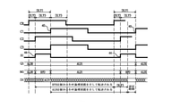
周波数信号C1は、フリップフロップ28に提供される。この例では、フリップフロップは、周波数信号C1の上がりエッジで組み合わせ論理回路24の出力D1をサンプリングする。フリップフロップ28のサンプリング時点は、40で示す。
・集積回路の設計及びそのタイミングの制限条件を静的タイミング解析ツールにロードする、例えばsynopsys社のPrimeTime又はIC compiler、
・回路設計のトレードオフによってタイミング均一化の制限条件(TBL)を設定する、
・組み合わせ論理回路24における出力ピンごとについて、
・このピンを通過する最小のスラックを有するタイミング経路を取得する、
・必要に応じて、遅延ユニットを増やして、最小経路タイミングのスラックが TBL より小さくなるまで遅延を増やす。
各実施例では、乱数生成器36は任意の適切なアナログ及び/又はデジタル回路で実現できる。乱数生成器36は、必ずしも周波数で駆動する必要がない、アナログノイズ源で実現しても良い。別の実施例では、乱数生成器36は、全デジタルハードウェアで実現でき、例えば、周波数論理を使用して擬似ランダムデータ列を生成する。いくつかの実施例では、乱数生成器36は、セーフティ電子デバイス20の固有するセキュリティ関連回路、例えばセキュア・ハッシュ・アルゴリズム(SHA)、又は高度暗号化規格(AES)暗号化エンジンを再利用しても良い。この場合には、毎回ランダムシードでSHA又は高度暗号化規格を実行したほうがいい。
図6は、本発明の更に別の実施例におけるサイドチャネル攻撃を防犯するセーフティ電子デバイスを示すブロック図である。図6は、図1~3の保護機構が追加のセキュリティ対策と組み合わせることができることを証明できる。図6は、一つの組み合わせ可能な対策を例として示す。
いくつかの実施例では、周波数期間ごとに、乱数生成器36はランダムデータを複数回修正する。例えば、図2の入力M1を参照し、間隔RPDにおけるランダムデータの数値は、少なくとも一回変更される。
24…組み合わせ論理回路
28、56、64、84、FF…フリップフロップ
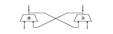
32,68,72…マルチプレクサ
36,80、RNG…乱数生成器
40,44…時点
48、DLY_G1、DLY_G2、DLY1、DLY2、DLY3…遅延ユニット
52…AES論理回路
60…SHA論理回路
ALD、ALD1、ALD2、ALD3…関数型データ
C1,C2,C3…周波数信号
CR…クロックツリー
G1,G2,G3…論理ゲート
L…論理レベル
M1…入力
MQ…サンプリングデータ
Q,D,D1…出力
Q1…関数型データ
R1,RPD、RPD1、RPD2、RPD3、RPDD、RPDD0、RPDD1、MD…ランダムデータ
S1…MUX制御信号
SRFF…SRのフリップフロップ
T_ALD_max…最大転送時間
T_ALD_min…最小転送時間
T_RPD_max…最大転送時間
T_RPD_min…最小転送時間
Claims (20)
- 少なくとも一つの入力及び少なくとも一つの出力を有する組み合わせ論理回路と、
複数の連続する周波数期間で前記組み合わせ論理回路の前記少なくとも一つの出力信号をサンプリングする少なくとも一つのステートサンプリングコンポーネントと、
保護回路と、を備え、
前記保護回路は、前記複数の周波数期間ごとに、
前記周波数期間における前記ステートサンプリングコンポーネントのサンプリング時間前に、所定の持続時間で前記組み合わせ論理回路の前記少なくとも一つの入力にランダムデータを提供し始める動作と、
前記ランダムデータを提供した後に、前記組み合わせ論理回路の前記少なくとも一つの入力に関数型データを提供するように変更して、前記ステートサンプリングコンポーネントにサンプリングをさせる動作とを実行することにより、前記組み合わせ論理回路を保護する、
前記組み合わせ論理回路における前記少なくとも一つの入力と前記少なくとも一つの出力との何れかの信号経路における転送遅延は、前記所定の持続時間以上であり、前記ステートサンプリングコンポーネントの前記サンプリング時間前に、前記所定の持続時間で前記ランダムデータが提供し始められることを特徴とする電子デバイス。 - 前記ランダムデータ及び前記関数型データは、前記ステートサンプリングコンポーネントに入力され、前記転送遅延は前記所定の持続時間以上であるので、前記ステートサンプリングコンポーネントは、前記ランダムデータをサンプリングしないで、前記関数型データのみをサンプリングすることを特徴とする請求項1に記載の電子デバイス。
- 前記組み合わせ論理回路は、少なくとも前記所定の持続時間に設定されるホールドタイム余裕度を有することを特徴とする請求項1に記載の電子デバイス。
- 前記組み合わせ論理回路は、前記ホールドタイム余裕度を少なくとも前記所定の持続時間に設定するための少なくとも一つの信号経路に挿入される遅延ユニットを少なくとも一つ含むことを特徴とする請求項3に記載の電子デバイス。
- 暗号化動作を実行するための第1の暗号化エンジン及び第2の暗号化エンジンを更に含み、前記保護回路は、前記第1の暗号化エンジンを使用して前記ランダムデータを生成するときは前記第2の暗号化エンジンを使用せず、かつ前記第2の暗号化エンジンを使用して前記ランダムデータを生成するときは前記第1の暗号化エンジンを使用せずに前記暗号化動作を実行することを特徴とする請求項1に記載の電子デバイス。
- 前記保護回路は、前記複数の周波数期間ごとに前記ランダムデータを複数回修正するために用いられることを特徴とする請求項1に記載の電子デバイス。
- 前記ランダムデータ及び前記関数型データを提供するためのタイミングは、前記電子デバイスにより事前に設定され、前記電子デバイスは、前記組み合わせ論理回路の独立性能に基づいて前記タイミングを事前に設定することを特徴とする請求項1に記載の電子デバイス。
- 前記保護回路は、前記組み合わせ論理回路の実際的な性能に基づいて、前記ランダムデータ及び前記関数型データを提供するためのタイミングを適応的に修正することを特徴とする請求項1に記載の電子デバイス。
- 前記保護回路は、前記タイミングを適応的に修正するので、前記ランダムデータを提供する動作期間を改善することを特徴とする請求項8に記載の電子デバイス。
- 前記関数型データを前記組み合わせ論理回路における前記少なくとも一つの入力に提供する前に、前記組み合わせ論理回路は、全ての前記信号経路における前記ランダムデータの転送を先に完了することを特徴とする請求項1に記載の電子デバイス。
- 電子デバイスにおける少なくとも一つの入力及び少なくとも一つの出力を有する組み合わせ論理回路を保護する方法であって、
複数の連続する周波数期間において、少なくとも一つのステートサンプリングコンポーネントを使用して前記組み合わせ論理回路における前記少なくとも一つの出力信号をサンプリングすることと、
前記複数の周波数期間ごとに、以下のようなステップを行って前記組み合わせ論理回路を保護すること、とを含み、
行うステップは、
前記周波数期間における前記ステートサンプリングコンポーネントのサンプリング時間前に、所定の持続時間で前記組み合わせ論理回路の前記入力にランダムデータを提供し始めるステップと、
前記ランダムデータを提供した後に、前記組み合わせ論理回路の入力に関数型データを提供するように変更して、前記ステートサンプリングコンポーネントにサンプリングをさせるステップと、を含み、
前記組み合わせ論理回路における前記少なくとも一つの入力と前記少なくとも一つの出力との何れかの信号経路における転送遅延は、前記所定の持続時間以上であり、前記ステートサンプリングコンポーネントの前記サンプリング時間前に、前記所定の持続時間で前記ランダムデータが提供し始められることを特徴とする電子デバイスにおける少なくとも一つの入力及び少なくとも一つの出力を有する組み合わせ論理回路を保護する方法。 - 前記ランダムデータ及び前記関数型データは、前記ステートサンプリングコンポーネントに入力され、前記転送遅延は前記所定の持続時間以上であるので、前記ステートサンプリングコンポーネントは、前記ランダムデータをサンプリングしないで、前記関数型データのみをサンプリングすることを特徴とする請求項11に記載の方法。
- 前記組み合わせ論理回路は、少なくとも前記所定の持続時間に設定されるホールドタイム余裕度を有することを特徴とする請求項11に記載の方法。
- 前記組み合わせ論理回路は、前記ホールドタイム余裕度を少なくとも前記所定の持続時間に設定するための少なくとも一つの信号経路に挿入される遅延ユニットを少なくとも一つ含むことを特徴とする請求項13に記載の方法。
- 前記電子デバイスは、暗号化動作を実行するための第1の暗号化エンジン及び第2の暗号化エンジンを含み、
前記ランダムデータを生成するステップは、
前記保護回路は、前記第1の暗号化エンジンを使用して前記ランダムデータを生成するときは前記第2の暗号化エンジンを使用せず、かつ前記第2の暗号化エンジンを使用して前記ランダムデータを生成するときは前記第1の暗号化エンジンを使用せずに前記暗号化動作を実行することを含むこと、
を特徴とする請求項11に記載の方法。 - 前記複数の周波数期間ごとに前記ランダムデータを複数回修正することを更に含むことを特徴とする請求項11に記載の方法。
- 前記電子デバイスの前記組み合わせ論理回路の独立性能に基づいて、前記ランダムデータ及び前記関数型データを提供するためのタイミングを事前に設定することを更に含むことを特徴とする請求項11に記載の方法。
- 前記組み合わせ論理回路の実際的な性能に基づいて、前記ランダムデータ及び前記関数型データを提供するためのタイミングを適応的に修正することを更に含むことを特徴とする請求項11に記載の方法。
- 前記タイミングを適応的に修正するステップは、
前記ランダムデータを提供する動作期間を改善することを含む
ことを特徴とする請求項18に記載の方法。 - 続き関数型データが前記組み合わせ論理回路の前記少なくとも一つの入力に提供される前に、前記組み合わせ論理回路の全ての前記信号経路における前記ランダムデータの転送を完了することを特徴とする請求項11に記載の方法。
Applications Claiming Priority (2)
| Application Number | Priority Date | Filing Date | Title |
|---|---|---|---|
| US16/194,342 US10878133B2 (en) | 2018-11-18 | 2018-11-18 | Mitigation of side-channel attacks using small-overhead random pre-charging |
| US16/194,342 | 2018-11-18 |
Publications (2)
| Publication Number | Publication Date |
|---|---|
| JP2020087453A JP2020087453A (ja) | 2020-06-04 |
| JP7005576B2 true JP7005576B2 (ja) | 2022-01-21 |
Family
ID=70727247
Family Applications (1)
| Application Number | Title | Priority Date | Filing Date |
|---|---|---|---|
| JP2019203511A Active JP7005576B2 (ja) | 2018-11-18 | 2019-11-08 | 小型オーバーヘッドランダムプリチャージを使用してサイドチャネル攻撃を防犯する電子デバイス |
Country Status (4)
| Country | Link |
|---|---|
| US (1) | US10878133B2 (ja) |
| JP (1) | JP7005576B2 (ja) |
| CN (1) | CN111200490B (ja) |
| TW (1) | TWI693791B (ja) |
Families Citing this family (7)
| Publication number | Priority date | Publication date | Assignee | Title |
|---|---|---|---|---|
| US20180089426A1 (en) * | 2016-09-29 | 2018-03-29 | Government Of The United States As Represented By The Secretary Of The Air Force | System, method, and apparatus for resisting hardware trojan induced leakage in combinational logics |
| JP6632773B1 (ja) * | 2018-12-14 | 2020-01-22 | 三菱電機株式会社 | 学習識別装置、学習識別方法、及び、学習識別プログラム |
| US11601120B2 (en) | 2021-02-03 | 2023-03-07 | Nuvoton Technology Corporation | Attack-resistant ring oscillators and random-number generators |
| US20220150046A1 (en) * | 2021-09-16 | 2022-05-12 | Intel Corporation | Deterring side channel analysis attacks for data processors having parallel cryptographic circuits |
| TWI818503B (zh) * | 2022-04-11 | 2023-10-11 | 新唐科技股份有限公司 | 加密裝置以及加密方法 |
| CN116743504B (zh) * | 2023-08-14 | 2023-10-17 | 佳瑛科技有限公司 | 一种数字数据在网络线缆中的安全传输方法及系统 |
| US12608470B2 (en) * | 2023-11-09 | 2026-04-21 | Microsoft Technology Licensing, Llc | Cyberattack countermeasure circuits and methods |
Citations (3)
| Publication number | Priority date | Publication date | Assignee | Title |
|---|---|---|---|---|
| JP2010219666A (ja) | 2009-03-13 | 2010-09-30 | Sony Corp | 暗号処理装置 |
| JP2014049891A (ja) | 2012-08-30 | 2014-03-17 | Renesas Electronics Corp | 中央処理装置および演算装置 |
| US20170061121A1 (en) | 2015-08-26 | 2017-03-02 | Cryptography Research, Inc | Low overhead random pre-charge countermeasure for side-channel attacks |
Family Cites Families (16)
| Publication number | Priority date | Publication date | Assignee | Title |
|---|---|---|---|---|
| JP3769940B2 (ja) * | 1998-08-06 | 2006-04-26 | 株式会社日立製作所 | 半導体装置 |
| US7840803B2 (en) * | 2002-04-16 | 2010-11-23 | Massachusetts Institute Of Technology | Authentication of integrated circuits |
| WO2005081085A2 (en) | 2004-02-13 | 2005-09-01 | The Regents Of The University Of California | Logic system for dpa and/or side channel attack resistance |
| US7577820B1 (en) * | 2006-04-14 | 2009-08-18 | Tilera Corporation | Managing data in a parallel processing environment |
| ATE440336T1 (de) | 2006-06-29 | 2009-09-15 | Incard Sa | Verfahren zum schutz von ic-karten vor leistungsanalyse-attacken |
| US7893742B2 (en) * | 2006-11-10 | 2011-02-22 | Nec Corporation | Clock signal dividing circuit |
| US8427194B2 (en) * | 2010-05-24 | 2013-04-23 | Alexander Roger Deas | Logic system with resistance to side-channel attack by exhibiting a closed clock-data eye diagram |
| US8983068B2 (en) * | 2013-03-06 | 2015-03-17 | Infineon Technologies Ag | Masked nonlinear feedback shift register |
| US10951391B2 (en) * | 2015-09-06 | 2021-03-16 | Bar-Ilan University | Randomized logic against side channel attacks |
| US10142103B2 (en) * | 2015-12-07 | 2018-11-27 | The Boeing Company | Hardware assisted fast pseudorandom number generation |
| IL243789A0 (en) * | 2016-01-26 | 2016-07-31 | Winbond Electronics Corp | Split calculation of the next state to prevent analysis by energy consumption |
| US10958414B2 (en) * | 2016-02-23 | 2021-03-23 | Google Llc | Clock period randomization for defense against cryptographic attacks |
| US10019571B2 (en) * | 2016-03-13 | 2018-07-10 | Winbond Electronics Corporation | Protection from side-channel attacks by varying clock delays |
| FR3051599A1 (fr) * | 2016-05-17 | 2017-11-24 | Stmicroelectronics Rousset | Protection d'un circuit integre |
| WO2018002939A1 (en) * | 2016-06-29 | 2018-01-04 | Bar-Ilan University | Pseudo-asynchronous digital circuit design |
| US10256973B2 (en) | 2016-09-30 | 2019-04-09 | Intel Corporation | Linear masking circuits for side-channel immunization of advanced encryption standard hardware |
-
2018
- 2018-11-18 US US16/194,342 patent/US10878133B2/en active Active
-
2019
- 2019-09-18 TW TW108133692A patent/TWI693791B/zh active
- 2019-09-23 CN CN201910897935.7A patent/CN111200490B/zh active Active
- 2019-11-08 JP JP2019203511A patent/JP7005576B2/ja active Active
Patent Citations (3)
| Publication number | Priority date | Publication date | Assignee | Title |
|---|---|---|---|---|
| JP2010219666A (ja) | 2009-03-13 | 2010-09-30 | Sony Corp | 暗号処理装置 |
| JP2014049891A (ja) | 2012-08-30 | 2014-03-17 | Renesas Electronics Corp | 中央処理装置および演算装置 |
| US20170061121A1 (en) | 2015-08-26 | 2017-03-02 | Cryptography Research, Inc | Low overhead random pre-charge countermeasure for side-channel attacks |
Also Published As
| Publication number | Publication date |
|---|---|
| US10878133B2 (en) | 2020-12-29 |
| JP2020087453A (ja) | 2020-06-04 |
| TWI693791B (zh) | 2020-05-11 |
| US20200159967A1 (en) | 2020-05-21 |
| CN111200490A (zh) | 2020-05-26 |
| CN111200490B (zh) | 2023-04-07 |
| TW202021276A (zh) | 2020-06-01 |
Similar Documents
| Publication | Publication Date | Title |
|---|---|---|
| JP7005576B2 (ja) | 小型オーバーヘッドランダムプリチャージを使用してサイドチャネル攻撃を防犯する電子デバイス | |
| Alam et al. | RAM-Jam: Remote Temperature and Voltage Fault Attack on FPGAs using Memory Collisions. | |
| JP5881715B2 (ja) | 開始挙動が改善された物理的複製不可能関数 | |
| De Cnudde et al. | Hardware masking, revisited | |
| US8495440B2 (en) | Fully programmable parallel PRBS generator | |
| Zussa et al. | Investigation of timing constraints violation as a fault injection means | |
| US20200342112A1 (en) | An autonomous, self-authenticating and self-contained secure boot-up system and methods | |
| US11728967B2 (en) | Dynamic masking | |
| US20140185795A1 (en) | Fuse attestation to secure the provisioning of secret keys during integrated circuit manufacturing | |
| Sutar et al. | D-PUF: An intrinsically reconfigurable DRAM PUF for device authentication and random number generation | |
| US20130073873A1 (en) | Signature generation apparatus, signature method, non-transitory computer readable medium storing signature generation program | |
| US12192319B2 (en) | Apparatus and method for modular multiplication resistant to side-channel attack | |
| Mentens | Hiding side-channel leakage through hardware randomization: A comprehensive overview | |
| Alioto et al. | Enabling ubiquitous hardware security via energy-efficient primitives and systems | |
| Igarashi et al. | Concurrent faulty clock detection for crypto circuits against clock glitch based DFA | |
| Muresan et al. | Power-smart system-on-chip architecture for embedded cryptosystems | |
| Choudhury et al. | Patron: A pragmatic approach for encoding laser fault injection resistant fsms | |
| WO2017216522A1 (en) | An apparatus and method for obfuscating power consumption of a processor | |
| US11906581B2 (en) | Hardware component and a method for implementing a camouflage of current traces generated by a digital system | |
| KR20200052808A (ko) | 시도 응답 방식의 물리적 복제방지 기능을 위한 집적 회로 및 이를 사용하는 방법 | |
| Rahman et al. | Design and security-mitigation of custom and configurable hardware cryptosystems | |
| Liu et al. | A low-overhead and high-reliability physical unclonable function (PUF) for cryptography | |
| Singh et al. | Mitigating power supply glitch based fault attacks with fast all-digital clock modulation circuit | |
| Billmann et al. | Open-source crypto ip cores for fpgas–overview and evaluation | |
| US20070147604A1 (en) | Integrated circuit having advanced encryption standard core and wrapper for validating advanced encryption standard core |
Legal Events
| Date | Code | Title | Description |
|---|---|---|---|
| A621 | Written request for application examination |
Free format text: JAPANESE INTERMEDIATE CODE: A621 Effective date: 20191108 |
|
| A977 | Report on retrieval |
Free format text: JAPANESE INTERMEDIATE CODE: A971007 Effective date: 20201225 |
|
| A131 | Notification of reasons for refusal |
Free format text: JAPANESE INTERMEDIATE CODE: A131 Effective date: 20210121 |
|
| A02 | Decision of refusal |
Free format text: JAPANESE INTERMEDIATE CODE: A02 Effective date: 20210914 |
|
| A521 | Request for written amendment filed |
Free format text: JAPANESE INTERMEDIATE CODE: A523 Effective date: 20211105 |
|
| C60 | Trial request (containing other claim documents, opposition documents) |
Free format text: JAPANESE INTERMEDIATE CODE: C60 Effective date: 20211105 |
|
| A911 | Transfer to examiner for re-examination before appeal (zenchi) |
Free format text: JAPANESE INTERMEDIATE CODE: A911 Effective date: 20211116 |
|
| C21 | Notice of transfer of a case for reconsideration by examiners before appeal proceedings |
Free format text: JAPANESE INTERMEDIATE CODE: C21 Effective date: 20211119 |
|
| TRDD | Decision of grant or rejection written | ||
| A01 | Written decision to grant a patent or to grant a registration (utility model) |
Free format text: JAPANESE INTERMEDIATE CODE: A01 Effective date: 20211214 |
|
| A61 | First payment of annual fees (during grant procedure) |
Free format text: JAPANESE INTERMEDIATE CODE: A61 Effective date: 20220105 |
|
| R150 | Certificate of patent or registration of utility model |
Ref document number: 7005576 Country of ref document: JP Free format text: JAPANESE INTERMEDIATE CODE: R150 |
|
| R250 | Receipt of annual fees |
Free format text: JAPANESE INTERMEDIATE CODE: R250 |
|
| R250 | Receipt of annual fees |
Free format text: JAPANESE INTERMEDIATE CODE: R250 |