JP7071055B2 - Image sensor and image sensor - Google Patents
Image sensor and image sensor Download PDFInfo
- Publication number
- JP7071055B2 JP7071055B2 JP2017033848A JP2017033848A JP7071055B2 JP 7071055 B2 JP7071055 B2 JP 7071055B2 JP 2017033848 A JP2017033848 A JP 2017033848A JP 2017033848 A JP2017033848 A JP 2017033848A JP 7071055 B2 JP7071055 B2 JP 7071055B2
- Authority
- JP
- Japan
- Prior art keywords
- photoelectric conversion
- conversion unit
- image pickup
- signal
- image
- Prior art date
- Legal status (The legal status is an assumption and is not a legal conclusion. Google has not performed a legal analysis and makes no representation as to the accuracy of the status listed.)
- Active
Links
Images






Classifications
-
- H—ELECTRICITY
- H10—SEMICONDUCTOR DEVICES; ELECTRIC SOLID-STATE DEVICES NOT OTHERWISE PROVIDED FOR
- H10F—INORGANIC SEMICONDUCTOR DEVICES SENSITIVE TO INFRARED RADIATION, LIGHT, ELECTROMAGNETIC RADIATION OF SHORTER WAVELENGTH OR CORPUSCULAR RADIATION
- H10F39/00—Integrated devices, or assemblies of multiple devices, comprising at least one element covered by group H10F30/00, e.g. radiation detectors comprising photodiode arrays
- H10F39/80—Constructional details of image sensors
- H10F39/802—Geometry or disposition of elements in pixels, e.g. address-lines or gate electrodes
-
- H—ELECTRICITY
- H04—ELECTRIC COMMUNICATION TECHNIQUE
- H04N—PICTORIAL COMMUNICATION, e.g. TELEVISION
- H04N23/00—Cameras or camera modules comprising electronic image sensors; Control thereof
- H04N23/10—Cameras or camera modules comprising electronic image sensors; Control thereof for generating image signals from different wavelengths
-
- H—ELECTRICITY
- H04—ELECTRIC COMMUNICATION TECHNIQUE
- H04N—PICTORIAL COMMUNICATION, e.g. TELEVISION
- H04N23/00—Cameras or camera modules comprising electronic image sensors; Control thereof
- H04N23/10—Cameras or camera modules comprising electronic image sensors; Control thereof for generating image signals from different wavelengths
- H04N23/12—Cameras or camera modules comprising electronic image sensors; Control thereof for generating image signals from different wavelengths with one sensor only
-
- H—ELECTRICITY
- H04—ELECTRIC COMMUNICATION TECHNIQUE
- H04N—PICTORIAL COMMUNICATION, e.g. TELEVISION
- H04N25/00—Circuitry of solid-state image sensors [SSIS]; Control thereof
- H04N25/70—SSIS architectures; Circuits associated therewith
- H04N25/76—Addressed sensors, e.g. MOS or CMOS sensors
- H04N25/77—Pixel circuitry, e.g. memories, A/D converters, pixel amplifiers, shared circuits or shared components
-
- H—ELECTRICITY
- H10—SEMICONDUCTOR DEVICES; ELECTRIC SOLID-STATE DEVICES NOT OTHERWISE PROVIDED FOR
- H10F—INORGANIC SEMICONDUCTOR DEVICES SENSITIVE TO INFRARED RADIATION, LIGHT, ELECTROMAGNETIC RADIATION OF SHORTER WAVELENGTH OR CORPUSCULAR RADIATION
- H10F39/00—Integrated devices, or assemblies of multiple devices, comprising at least one element covered by group H10F30/00, e.g. radiation detectors comprising photodiode arrays
- H10F39/80—Constructional details of image sensors
- H10F39/805—Coatings
- H10F39/8053—Colour filters
-
- H—ELECTRICITY
- H10—SEMICONDUCTOR DEVICES; ELECTRIC SOLID-STATE DEVICES NOT OTHERWISE PROVIDED FOR
- H10F—INORGANIC SEMICONDUCTOR DEVICES SENSITIVE TO INFRARED RADIATION, LIGHT, ELECTROMAGNETIC RADIATION OF SHORTER WAVELENGTH OR CORPUSCULAR RADIATION
- H10F39/00—Integrated devices, or assemblies of multiple devices, comprising at least one element covered by group H10F30/00, e.g. radiation detectors comprising photodiode arrays
- H10F39/80—Constructional details of image sensors
- H10F39/806—Optical elements or arrangements associated with the image sensors
-
- H—ELECTRICITY
- H10—SEMICONDUCTOR DEVICES; ELECTRIC SOLID-STATE DEVICES NOT OTHERWISE PROVIDED FOR
- H10F—INORGANIC SEMICONDUCTOR DEVICES SENSITIVE TO INFRARED RADIATION, LIGHT, ELECTROMAGNETIC RADIATION OF SHORTER WAVELENGTH OR CORPUSCULAR RADIATION
- H10F39/00—Integrated devices, or assemblies of multiple devices, comprising at least one element covered by group H10F30/00, e.g. radiation detectors comprising photodiode arrays
- H10F39/80—Constructional details of image sensors
- H10F39/806—Optical elements or arrangements associated with the image sensors
- H10F39/8063—Microlenses
-
- H—ELECTRICITY
- H10—SEMICONDUCTOR DEVICES; ELECTRIC SOLID-STATE DEVICES NOT OTHERWISE PROVIDED FOR
- H10K—ORGANIC ELECTRIC SOLID-STATE DEVICES
- H10K19/00—Integrated devices, or assemblies of multiple devices, comprising at least one organic element specially adapted for rectifying, amplifying, oscillating or switching, covered by group H10K10/00
- H10K19/20—Integrated devices, or assemblies of multiple devices, comprising at least one organic element specially adapted for rectifying, amplifying, oscillating or switching, covered by group H10K10/00 comprising components having an active region that includes an inorganic semiconductor
Landscapes
- Engineering & Computer Science (AREA)
- Multimedia (AREA)
- Signal Processing (AREA)
- Chemical & Material Sciences (AREA)
- Inorganic Chemistry (AREA)
- Solid State Image Pick-Up Elements (AREA)
- Transforming Light Signals Into Electric Signals (AREA)
Description
本発明は、撮像素子および撮像素子を備える撮像装置に関する。 The present invention relates to an image pickup device and an image pickup device including the image pickup element.
近年、有機光電変換膜とシリコン光電変換部とを積層した構成の撮像素子を用いて、色再現性と高精細性を向上する試みが提案されている。この撮像素子においては、有機光電変換膜での吸収波長帯域以外の波長帯域の光、つまり補色となる帯域の光をシリコン光電変換部で吸収することが提案されている。 In recent years, there have been proposed attempts to improve color reproducibility and high definition by using an image pickup device having a structure in which an organic photoelectric conversion film and a silicon photoelectric conversion unit are laminated. In this image pickup device, it has been proposed that the silicon photoelectric conversion unit absorbs light in a wavelength band other than the absorption wavelength band in the organic photoelectric conversion film, that is, light in a band that becomes a complementary color.
例えば、特許文献1では、市松状に配列されたシアンとイエローのカラーフィルターの下に、緑色の波長帯域が吸収帯域となる一様な有機光電変換膜、その下にシリコン光電変換部が形成された撮像素子が提案されている。この場合、シアンおよびイエローの各カラーフィルターを透過した光のうち緑色の波長帯域の光を有機光電変換膜で吸収して信号へ変換し、ここで吸収されなかった各青色と赤色の波長帯域の光をシリコン光電変換部で吸収して信号へ変換する。また、特許文献2では、カラーフィルターを有さない撮像素子が提案されており、上部に設けられた第一の光電変換部として緑色の波長帯域の光に対して吸収を示す有機光電変換膜、その下にシリコン基板上に形成された第2および第3の光電変換部が形成されている。有機光電変換膜を透過した青色と赤色の波長帯域の光は、第2の光電変換部に進入する。しかし、シリコン基板中での青色の波長帯域の光の吸収係数が赤色のそれよりも大きいことから、浅い領域では青色の波長帯域の光が吸収される。そして、深い領域ほど赤色の波長帯域の光が吸収されることになる。つまり、第2の光電変換部において青色の波長帯域の光が十分に吸収され、第3の光電変換部においては赤色の波長帯域の光の多くが吸収される。このように、第2および第3の光電変換部の位置と厚さを決定しておけば、3層に亘る光電変換部での信号を取得できることになる。
For example, in
しかしながら、上述の特許文献に開示された従来技術では、積層された光電変換部において異なる色の波長帯域の光を吸収することになるため、同じ波長帯域の光の信号を同時に取得することができない。つまり、動画を撮像しながら同時に静止画を撮像するようなことができない。さらに、撮像の波長帯域に相当する光による撮像面位相差方式の高速な焦点検出を行うことができない。 However, in the prior art disclosed in the above-mentioned patent document, since the laminated photoelectric conversion units absorb light in different color wavelength bands, it is not possible to simultaneously acquire light signals in the same wavelength band. .. That is, it is not possible to capture a still image at the same time as capturing a moving image. Further, it is not possible to perform high-speed focus detection of the imaging surface phase difference method using light corresponding to the wavelength band of imaging.
そこで、本発明の目的は、可視光帯域の光に対する高精度かつ高速な焦点検出、および可視光帯域における二つの同時撮像を可能にした、撮像素子および撮像装置を提供することである。 Therefore, an object of the present invention is to provide an image pickup device and an image pickup apparatus capable of high-precision and high-speed focus detection for light in the visible light band and two simultaneous imaging in the visible light band.
上記目的を達成するために、本発明は、撮像面上に複数の撮像画素を備える撮像素子であって、前記複数の撮像画素は、外部からの光を画素内部に導くためのマイクロレンズと、所定の波長帯域の光を透過するカラーフィルターと、前記カラーフィルターを透過した光を光電変換するための第1の光電変換部と、前記第1の光電変換部の下方に所定の間隔を有して設けられた第2の光電変換部と、を有し、前記第1の光電変換部は前記複数の画素で共通した膜層を含み、前記第1の光電変換部には前記第1の光電変換部の一部の領域から第1の信号を取得するための第1の電極と、前記一部の領域とは異なる領域から第2の信号を取得する第2の電極が設けられ、前記第1の光電変換部の前記所定の波長帯域における光の透過率は、50%よりも大きく、前記第1の光電変換部の前記膜層の厚みは前記複数の画素に亘って一様であり、前記第1の光電変換部において吸収される各色の光強度の比と前記第2の光電変換部において吸収される各色の光強度の比が同程度となるように前記カラーフィルターの厚さを色ごとに設定することを特徴とする。
In order to achieve the above object, the present invention is an image pickup element provided with a plurality of image pickup pixels on an image pickup surface, wherein the plurality of image pickup pixels are a microlens for guiding light from the outside into the pixel. A color filter that transmits light in a predetermined wavelength band, a first photoelectric conversion unit for photoelectrically converting light transmitted through the color filter, and a predetermined space below the first photoelectric conversion unit. The first photoelectric conversion unit includes a film layer common to the plurality of pixels, and the first photoelectric conversion unit includes the first photoelectric conversion unit. A first electrode for acquiring a first signal from a part of a region of the conversion unit and a second electrode for acquiring a second signal from a region different from the part of the region are provided. The light transmission rate of the
本発明によれば、可視光帯域の光に対する高精度かつ高速な焦点検出をしながら、可視光帯域における二つの撮像を同時に可能にした、撮像素子および撮像装置を提供することができる。 According to the present invention, it is possible to provide an image pickup device and an image pickup apparatus capable of simultaneously performing two images in the visible light band while performing high-precision and high-speed focus detection for light in the visible light band.
以下、添付図面を参照して本発明を実施するための形態を詳細に説明する。ただし、本形態において例示される構成要素の寸法、材質、形状、それらの相対配置などは、本発明が適用される装置の構成や各種条件により適宜変更が可能であり、本発明がそれらの例示に限定されるものではない。 Hereinafter, embodiments for carrying out the present invention will be described in detail with reference to the accompanying drawings. However, the dimensions, materials, shapes, relative arrangements, etc. of the components exemplified in the present invention can be appropriately changed depending on the configuration of the apparatus to which the present invention is applied and various conditions, and the present invention exemplifies them. Not limited to.
(第1の実施形態)
本発明の撮像素子の実施形態として、有効画素領域の水平方向サイズ22.32ミリメートル、垂直方向サイズ14.88ミリメートル、水平方向の有効画素数6000、垂直方向の有効画素数4000のものを挙げる。図1(a)は、撮像素子の撮像面上に配列された複数の撮像画素の一部として2行2列分の基本画素群101を表す模式図である。基本画素群101は、赤色相当の波長帯域に分光感度を有する画素(R画素)102、青色相当の波長帯域に分光感度を有する画素(B画素)103を備える。さらに、緑色相当の波長帯域に分光感度を有する二つの画素(G画素)104と105により構成されているものとする。
(First Embodiment)
Examples of the image pickup device of the present invention include a horizontal size of 22.32 mm, a vertical size of 14.88 mm, a horizontal effective pixel count of 6000, and a vertical effective pixel count of 4000 mm in the effective pixel region. FIG. 1A is a schematic diagram showing a
図1(b)中の106は本発明の撮像素子を撮像面上方から見た模式図であり、基本画素群101が、撮像面上に2次元状に配列されている。説明のため、本明細書では複数の撮像画素が配列された撮像面をx-y面に平行とし、これに垂直な方向をz方向とする。
106 in FIG. 1B is a schematic view of the image pickup device of the present invention viewed from above the image pickup surface, and the
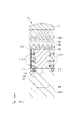
ここで、基本画素群101をなす撮像画素102、103、104、105の基本的な構成はカラーフィルター206以外同一として、撮像画素の構成を説明するために撮像画素102に着目する。図1(a)中の撮像画素102について、z-x面における画素の断面を図2に示す。
Here, the basic configurations of the
n型シリコン基板201には、その表面側にイオン注入により形成された第2の光電変換部202が設けられている。第2の光電変換部202の上方(z方向)には、光導波路203を挟んで第1の光電変換部204が積層されている。第1の光電変換部204の上方にはカラーフィルター206、および撮像画素に入射される光を画素内部に集光しながら導くためのマイクロレンズ207が設けられている。
The n-
転送ゲート214は、第2の光電変換部202において光電変換された電荷をコンデンサー213へ転送するために設けられている。コンデンサー213に転送された電荷は電圧信号に変換される。本実施形態において第2の光電変換部202において取得される信号は撮像信号として画像生成処理に用いられる。
The
光導波路203は、x-y面内で光導波路203の外側の屈折率実部よりも内側の屈折率実部が大きくなるように構成されている。光導波路内部は可視光に対して透明であり、前述の屈折率実部の関係を満たすものであれば様々な高屈折材料で構成されてよい。例えば、光導波路外部をSiOx、内部をSiNxで構成するなど挙げられるがこれに限るものではない。
The
第1の光電変換部204上部には周囲の画素上にまたがるように形成された上部透明電極205が形成されている。さらに、第1の光電変換部204下部には周囲の画素とは電気的に分離した下部透明電極208および209が形成されている。下部透明電極208と209の電極パターンは、入射光学系の瞳領域を分割およびパターン化することに相当している。そして、分割およびパターン化された異なる瞳領域を通過して入射される光束に属する光を光電変換して電荷を生成し、それぞれ対応する下部透明電極を通して前述の電荷を電気信号として出力することが可能である。これら異なる下部透明電極からの電気信号は光学的に瞳分割された光束に対応する信号である。本実施形態において、第1の光電変換部において取得される信号は瞳分割による位相差方式の焦点検出処理に用いられる。
An upper
なお、第1の光電変換部204は、可視光帯域において受光感度が確保される限り、有機光電変換膜や量子ドットフィルムなど様々なものが適応可能であり、特に可視光帯域において一定の受光感度となるものが望ましい。本実施形態では、第1の光電変換部204を有機光電変換膜で構成しており、上部透明電極との間に電子ブロック層、下部透明電極との間にホールブロック層など効率的に電荷を電極へ輸送するための層構造が形成されている。また、第1の光電変換部204は、複数の画素で共通した膜層となっている。
As long as the light receiving sensitivity is secured in the visible light band, various materials such as an organic photoelectric conversion film and a quantum dot film can be applied to the first
光導波路203の両側には電気配線部210と211が設けられている。電気配線部210及び211は、信号電荷の読み取りやスイッチングを行うための信号を各素子に伝送するために用いられる。また、電気配線部210と211は光導波路203の外側の低屈折材料で覆われて、絶縁されている。そして、コンデンサー213等のn型シリコン基板201に設けられた各素子を遮光する機能も有する。
本発明において、第1の光電変換部204の厚さを、第1の光電変換部204に入射する光(特に可視光)のうち50%以下を吸収し(透過率が50%よりも大きい)、それ以外を透過させるように設定する。本実施形態では、所定の割合がおよそ10%となるように設定してあるものとする。しかし、この設定に限られるものではなく、第1の光電変換部204で吸収する光に対して透過する光の割合を所定の割合とすればよい。これは、第1の光電変換部204のから取得される信号から記録される画像生成し、その上方の第2の光電変換部202から取得される信号から焦点検出を行うためである。焦点検出には一時的に用いるにすぎないため、第1の光電変換部204における吸収率を50%以下とした。したがって、第1の光電変換部204の光を吸収する割合はそれぞれの光電変換部から出力される信号の用途に基づいて決定されることが好ましい。
In the present invention, the thickness of the first
本実施形態では、第1の光電変換部204から出力される信号を例えば周辺の同色撮像画素の9画素で加算して用いる。そのため、第1の光電変換部204において光を約10%しか吸収しない場合であって、加算する十分な信号強度を確保することができる。これに対して第2の光電変換部202へは、散乱や細かな吸収を無視して考えると、カラーフィルター206からの光のうちおよそ90%を受光することができる。そのため、周辺同色画素間での信号加算を行わず、高解像度の画像を第2の光電変換部202を用いて取得することができる。ここで、第1の光電変換部204から出力される信号は加算するために、第2の光電変換部202より取得する画像よりも低解像度となる。つまり、第1の光電変換部204の1画素にあたる面積が、第2の光電変換部202の1画素の面積よりも広くなる。
In the present embodiment, the signal output from the first
なお、本実施形態においては加算数(加算単位)を9画素としたが、2以上の画素を加算すれば同様の効果を得ることが可能である。ここで、第1の光電変換部204における透過率の逆数と加算数の逆数を略同一とすることで、第1の光電変換部204から得られる信号と第2の光電変換部202から得られる信号との出力レベルをそろえることが可能となる。
In this embodiment, the number of additions (addition unit) is 9 pixels, but the same effect can be obtained by adding 2 or more pixels. Here, by making the reciprocal of the transmittance in the first
また、本実施形態では、第1の光電変換部204と第2の光電変換部202から信号を取得する周期であるフレームレートが異なる。具体的には第1の光電変換部204から信号を取得する周期は第2の光電変換部202から信号を取得する周期よりも早く設定される。これによって、低解像度であるが高フレームレートでの焦点調節と撮像(動画撮やライブビュー(LV)撮像)を行うと同時に、その最中の任意のタイミングで相対的に高解像度であるがやや低フレームレートでの撮像(静止画撮像)を実現することができる。言い換えれば、第1の光電変換部204の信号をLV撮像や動画撮像に用いることで常時高速な焦点調節を実現し、第2の光電変換部202の信号を用いた静止画撮像を行うことが可能となる。
Further, in the present embodiment, the frame rates, which are the cycles for acquiring signals from the first
図3は、カラーフィルター206を透過した後の光強度の波長依存性つまりカラーフィルター206の透過スペクトルの模式的グラフである。例えば、このスペクトルのピーク波長λ0における第1の光電変換部204(有機光電変換膜)の吸収係数をα(λ0)[/nm]とした場合、厚さt[nm]の光電変換膜を透過した後の波長λ0の光強度はexp(-α(λ0)・t)となる。そのため、このような式を用いて光電変換膜の厚さを決定することが可能である。ただし、ピーク波長に注目する方法ではなく、波長全体にわたって光強度を積分した場合の透過割合で決める方法など、ここに記載の方法に限るものではないし、複数の方法を組み合わせてもよい。
FIG. 3 is a schematic graph of the wavelength dependence of the light intensity after passing through the
前述のように、光電変換膜の吸収係数αは、波長λに依存するため、R、G、Bのカラーフィルター206を透過した後の光に対する吸収係数もそれぞれ異なる。これに対して、配置される光電変換膜の厚さは基本的に撮像素子全体に亘って一様であるため、R、G,Bの画素において光電変換膜に入射する光の強度が一定だとしても、光電変換膜を透過する光の強度はR、G、Bの画素間で異なってしまう。つまり、光電変換膜で得られる光強度のRGB比と第2の光電変換部202で得られる光強度のRGB比が異なってしまう。
As described above, since the absorption coefficient α of the photoelectric conversion film depends on the wavelength λ, the absorption coefficient for light after passing through the
このような場合、例えばカラーフィルター206の厚さを調整する方法により第1の光電変換部204と第2の光電変換部202において吸収される光強度のRGB比を同程度または近い値にすることが可能である。ただし、すべての波長帯域(RGB)のカラーフィルター206の厚さでのRGB比の設定が難しい場合もある。この場合は、着目する2つの波長帯域(たとえば、GとRなど)のRGBが光電変換部での吸収と透過光強度で合うように、2つのカラーフィルター206の厚さの関係を設定することも可能である。
In such a case, for example, by adjusting the thickness of the
さらに他の方法としては、光電変換膜における焦点検出に重要な緑色の波長帯域に着目して、この波長帯域の光の光電変換膜での吸収と透過の比を光電変換膜の厚さで設定するなどの方法が有効である。 As yet another method, focusing on the green wavelength band, which is important for focus detection in the photoelectric conversion film, the ratio of absorption and transmission of light in this wavelength band in the photoelectric conversion film is set by the thickness of the photoelectric conversion film. A method such as doing is effective.
他にも、光電変換膜の吸収スペクトルにおいて吸収の小さい波長帯域に相当する色の画素において光電変換膜での吸収と透過の比が所定の値(本実施形態では1:9)となるように、第1の光電変換部204の膜の厚さを設定するなどの方法も有効である。逆に吸収の大きい波長帯域に着目することで、吸収の小さい波長帯域の光は十分に透過させることができる。
In addition, in the absorption spectrum of the photoelectric conversion film, the ratio of absorption to transmission in the photoelectric conversion film is set to a predetermined value (1: 9 in this embodiment) in the pixels of the color corresponding to the wavelength band where the absorption is small. , It is also effective to set the thickness of the film of the first
さらに、各R、G、B画素においてカラーフィルター206を透過した光のうち最も強度の高い波長帯域の光に着目して、光電変換膜での吸収と透過の比を光電変換膜の厚さで設定することも可能である。
Furthermore, focusing on the light in the wavelength band with the highest intensity among the light transmitted through the
いくつかの方法により、光電変換膜での吸収光と透過光の強度のRGB比を調整したとしても、吸収と透過ではRGB比がずれる場合がある。このような場合には、あらかじめずれ量を検知しておき、光電変換膜からの出力信号と、第2の光電変換部202からの出力信号の間で、撮像後に補正量として与えることで、二つの画像を補正することが可能である。
Even if the RGB ratio of the intensity of the absorbed light and the transmitted light in the photoelectric conversion film is adjusted by some methods, the RGB ratio may be different between the absorption and the transmission. In such a case, the amount of deviation is detected in advance, and the output signal from the photoelectric conversion film and the output signal from the second
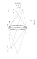
図4は、本実施形態の撮像素子を構成する像高中央付近の撮像画素において光の集光の様子を表す模式図である。撮像画素102外部からマイクロレンズに向かって矢印群401で示すように平行光が入射する場合を示している。この入射光401は画素内部で集光点402を形成し、この集光点402がz方向において第1の光電変換部204の中央付近、かつx方向において下部透明電極208と209の間に位置するように設定されている。ここで集光点とは、光束断面を円形と仮定した場合にその径が最も小さくなる領域を含む微小領域を称し、例えばガウシアンビームにおけるビームウェスト領域に相当する。したがって、マイクロレンズ207の焦点位置は第1の光電変換部204のz方向の位置と略一致すると言える。
FIG. 4 is a schematic diagram showing a state of light collection in an image pickup pixel near the center of the image height constituting the image pickup device of the present embodiment. The case where parallel light is incident from the outside of the
なお、本実施形態では、x方向に分割された下部透明電極208と209の間に集光点が位置するよう設定されているが、下部透明電極の分割方向はx方向に限るものではない。例えば、着目する瞳分割方向において位相差検出に携わる下部透明電極対の間に位置するようx-y面内で集光点を設定することが好ましい。
In the present embodiment, the condensing point is set to be located between the lower
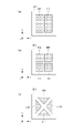
本実施形態では、図5(a)に示すように、x-y面内において画素領域501の中でx方向に分割された二つの下部透明電極502及び503により瞳分割を行っている。ただし本発明では、図5(b)における下部透明電極504、505、506および507、図5(c)における下部透明電極508、509、510および511のようにxおよびy方向の量方向に瞳分割を行うことも可能である。つまり、瞳分割の方向や分割数および下部透明電極の形状は限定されるものではない。上部および下部透明電極の材料としては、例えばフッ素ドープ酸化スズ(FTO)やスズドープ酸化インジウム(ITO)などが挙げられるがこれらに限るものではない。
In this embodiment, as shown in FIG. 5A, pupil division is performed by two lower
また、本発明の撮像素子における第2の光電変換部202における露光時間を制御するため、撮像素子には電子シャッター機構が組み込まれている。なお、本実施形態では、撮像素子をなす撮像画素の第2の光電変換部202には露光時間制御のためのグローバルシャッター機構が組み込まれているものとする。具体的には、第2の光電変換部202で発生した電荷を、転送ゲート214をコンデンサー213に転送する。この転送タイミングを撮像素子内の複数の画素において同一タイミングとすることで、グローバルシャッターを用いて撮像を実現することが可能となる。このように、第2の光電変換部202の信号を用いる静止画撮像にかかる露光をグローバルシャッター機構を用いて行うことにより、第1の光電変換部204の信号を用いた動画撮像中であっても、ローリングシャッター歪の少ない静止画撮像を行うことが出来る。
Further, in order to control the exposure time in the second
本実施形態の撮像素子と瞳分割との対応関係を示した概略図を図6に示す。線604は、像を取得する被写体の位置(面)を示し、位置605にある撮像光学系を通して被写体像を撮像素子表面位置606に形成する。また609は撮像素子をなす撮像画素の第1の光電変換部204のz方向における中央付近を表す。撮像素子の画素毎に、x方向に2分割された下部透明電極601に対応する光電変換部と下部透明電極602に相当する光電変換部は、それぞれ、瞳部分領域607と瞳部分領域608の異なる瞳部分領域を通過する光束を受光する。
FIG. 6 shows a schematic diagram showing the correspondence between the image pickup device and the pupil division of the present embodiment. The
画素毎に下部透明電極601に対応する光電変換部と下部透明電極602に相当する光電変換部の中から特定の光電変換部の信号を選び出す。そして、結像光学系の瞳部分領域607と瞳部分領域608の中の特定の瞳部分領域に対応した視差画像を得ることができる。例えば、画素毎に、下部透明電極602に対応する光電変換部の信号を選び出すことで、結像光学系の瞳部分領域607に対応した有効画素数の解像度の視差画像を得ることができる。下部透明電極603に相当する光電変換部でも同様である。
A signal of a specific photoelectric conversion unit is selected from the photoelectric conversion unit corresponding to the lower
また、画素毎に下部透明電極602に対応する光電変換部と下部透明電極603に相当する光電変換部の信号を加算することで、有効画素数の解像度の撮像画像を生成することができる。
Further, by adding the signals of the photoelectric conversion unit corresponding to the lower
なお本実施形態では、図6のように撮像素子の中央から遠い撮像画素ほどそのマイクロレンズの位置が撮像画素の中央側へ偏芯している。これは、撮像素子の中央から遠い部分では結像光学系からの主光線の方向がより傾くため、この傾きに対応するためである。 In this embodiment, as shown in FIG. 6, the position of the microlens of the image pickup pixel farther from the center of the image pickup element is eccentric toward the center side of the image pickup pixel. This is because the direction of the main light beam from the imaging optical system is more inclined in the portion far from the center of the image pickup device, and this is to cope with this inclination.
続いて、本発明における視差画像の像ずれ量とデフォーカス量の関係について説明する。 Subsequently, the relationship between the amount of image shift and the amount of defocus of the parallax image in the present invention will be described.
図7に、視差画像間の像ずれ量とデフォーカス量の概略関係図を示す。撮像面606に本実施形態の撮像素子(不図示)が配置され、図6と同様に、結像光学系の射出瞳が、瞳部分領域607と瞳部分領域608に2分割される場合を想定する。
FIG. 7 shows a schematic relationship diagram between the amount of image shift and the amount of defocus between parallax images. It is assumed that the image pickup device (not shown) of the present embodiment is arranged on the
デフォーカス量dは、被写体の結像位置から撮像面までの距離を大きさ|d|、被写体の結像位置が撮像面より被写体側にある前ピン状態を負符号(d<0)、被写体の結像位置が撮像面より被写体の反対側にある後ピン状態を正符号(d>0)として定義する。被写体の結像位置が撮像面にある合焦状態はd=0である。図7で、被写体701は合焦状態(d=0)の例を示しており、被写体702は前ピン状態(d<0)の例を示している。前ピン状態(d<0)と後ピン状態(d>0)を合わせて、デフォーカス状態(|d|>0)とする。 The defocus amount d is the distance from the imaging position of the subject to the imaging surface | d |, the front pin state in which the imaging position of the subject is closer to the subject than the imaging surface is a minus sign (d <0), and the subject. The rear pin state in which the image formation position of is on the opposite side of the subject from the image pickup surface is defined as a plus sign (d> 0). The in-focus state in which the image formation position of the subject is on the image pickup surface is d = 0. In FIG. 7, the subject 701 shows an example of the in-focus state (d = 0), and the subject 702 shows an example of the front pin state (d <0). The front pin state (d <0) and the rear pin state (d> 0) are combined to obtain a defocus state (| d |> 0).
前ピン状態(d<0)では、被写体702からの光束のうち、瞳部分領域607(608)を通過した光束は、一度、集光した後、光束の重心位置G1(G2)を中心として幅P1(P2)に広がり、撮像面606でボケた像となる。ボケた像は、下部透明電極601に対応する光電変換部と下部透明電極602に相当する光電変換部により受光され、視差画像が生成される。よって、下部透明電極601に対応する光電変換部と下部透明電極602に相当する光電変換部の信号から生成される視差画像には、重心位置G1(G2)に、被写体702が幅P1(P2)にボケた被写体像として記録される。被写体像のボケ幅P1(P2)は、デフォーカス量dの大きさ|d|が増加するのに伴い、概ね、比例して増加していく。同様に、視差画像間の被写体像の像ずれ量p(=G1-G2)の大きさ|p|も、デフォーカス量dの大きさ|d|が増加するのに伴い、概ね、比例して増加していく。後ピン状態(d>0)でも、視差画像間の被写体像の像ずれ方向が前ピン状態と反対となるが、同様である。合焦状態(d=0)では、視差画像間の被写体像の重心位置が一致(p=0)し、像ずれは生じない。
In the front pin state (d <0), among the luminous fluxes from the subject 702, the luminous flux that has passed through the pupil portion region 607 (608) is once focused and then has a width centered on the center of gravity position G1 (G2) of the luminous flux. It spreads over P1 (P2) and becomes a blurred image on the
したがって、下部透明電極601に対応する光電変換部と下部透明電極602に相当する光電変換部の信号を用いる。これにより得られる二つ(複数)の視差画像において、視差画像のデフォーカス量の大きさが増加するのに伴い、複数の視差画像間の像ずれ量の大きさが増加する。本実施形態の撮像素子の第1の光電変換部からの信号を用いて視差画像間の像ずれ量を相関演算により算出することで、瞳分割による位相差検出方式の焦点検出信号を用いた焦点検出を行うことができる。
Therefore, the signals of the photoelectric conversion unit corresponding to the lower
(第2の実施形態)
本発明の撮像素子の第2の実施形態として、第1の実施形態と同様の有効画素数及び画素配列を有する。撮像素子の撮像面上の基本画素群101の並びも実施形態と同等とし、基本画素群101が、撮像面上に2次元状に配列されている。ただし、基本画素群101をなす各撮像画素の内部構造の詳細は実施形態と異なるため、以下詳細に説明する。
(Second embodiment)
As a second embodiment of the image pickup device of the present invention, it has the same number of effective pixels and pixel arrangement as the first embodiment. The arrangement of the
本実施形態において、基本画素群101をなす各撮像画素の基本的な構成はカラーフィルター206以外同一である。本実施形態に係る画素における断面図について図8に示す。第1の実施形態における第2の光電変換部202に相当する光電変換部として、本実施形態においては第2の光電変換膜902が設けられている。そして、第1の光電変換部904および第2の光電変換膜902の間には、共通した電極である共通電極905が配置されている。そして、第1の光電変換部904の上面には、第1の実施形態における下部透明電極208および209に相当する、瞳分割による位相差検出方式の焦点検出に携わる分割された上部透明電極908および909が配置されている。なお、図8の断面においては、第1の光電変換部904と第2の光電変換部902は画素毎に区切られているが、製造する上では、夫々画素毎に共通の膜層とすることが好ましい。
In the present embodiment, the basic configuration of each image pickup pixel forming the
上部透明電極908及び909は、それぞれ個別にコンデンサー914および912に接続されて読出し回路へ接続されている。第2の光電変換部902の下面には、下部透明電極903が配置されている。下部透明電極903はTi/Cu等の一様電極が形成され、第2の光電変換部902で発生した電荷をコンデンサー913に送るよう設定されている。下部透明電極903は、その下へ光を透過させる必要がないため必ずしも透明電極でなくてよく、シリコン基板901上に設けられた各素子への入射光の影響を低減するための遮光部としての役割も有する。本実施形態では、第1の光電変換部904において入射光が透過する所定の割合がおよそ90%となるように膜厚等を設定してあるものとする。本実施形態では、第1の光電変換部904からの信号を周辺の同色撮像画素の9画素で加算して用いるため、第1の光電変換部904において光を10%しか吸収しないとしても、加算するために十分な信号強度を確保することができる。一方で、これに対して第2の光電変換部902へは、散乱や細かな吸収を無視して考えると、カラーフィルター206からの光のうちおよそ90%を受光することができる。そのため、周辺同色画素間での信号加算を行わず、高解像度の撮像を第2の光電変換部902を用いて行うことができる。このように所定の割合を設定することで、第1の光電変換部904を用いて相対的にやや低解像度であるが高フレームレートでの焦点調節と撮像(動画撮像やライブビュー(LV)撮像)を実現できる。さらに、上記動作中の任意のタイミングで相対的に高解像度であるがやや低フレームレートでの撮像(静止画撮像)も実現することができる。
The upper
本実施形態における画素内部における光の集光点は、z方向において第1の光電変換部904の中央付近、かつx方向において上部透明電極908、909の間に位置するように設定されている。本実施形態では、x方向に分割された下部透明電極908、909の間に集光点が位置するよう設定されている。しかし、上部透明電極の分割方向はx方向に限るものではく、着目する瞳分割方向において位相差検出に携わる上部透明電極対の間に位置するようx-y面内で集光点を設定することが好ましい。
The light focusing point inside the pixel in the present embodiment is set to be located near the center of the first
(第3の実施形態)
本発明の撮像装置の具体的な構成例を第2の実施形態として以下に図を用いて説明する。図9は、本実施形態にかかる撮像装置の機能構成例を示すブロック図であり、実施形態で説明した撮像素子106を有するものである。一例としてはデジタルカメラであるが、撮像素子を有し撮像する機能を有する、携帯電話、監視カメラ、移動体カメラ等であってもよい。本実施形態の撮像装置では、撮像素子106の第1の光電変換部904からの二つの視差画像を瞳分割による位相差検出方式の焦点調節に用いると同時に、動画撮像、LV撮像に用いる。この際、同色周辺の9画素における分割された下部透明電極のうち同一配置のものから得られる信号を加算する。第1の光電変換部904の信号を用いた画像は、9画素を1画素に加算処理していることから解像度は低下するが、高速な焦点調節が可能である。第1の光電変換部904を透過し下方の第2の光電変換部902にて受光された光に基づく信号は、静止画撮像に用いられる。カラーフィルター206の透過後の約90%光が、所定の間隔離間した第2の光電変換部902に光導波路を介して到達する。そのため、第2の光電変換部902からは第1の光電変換部904で得られる信号の約9倍という大きな信号が得られ、静止画撮像では画素間の信号加算を行わず、高解像度の画像を得ることが可能である。静止画撮像では、撮像素子駆動回路823を通してグローバルシャッター撮像が行われ、ローリングシャッターなどに起因する画像歪を極力抑制することが可能である。
(Third embodiment)
A specific configuration example of the image pickup apparatus of the present invention will be described below with reference to a second embodiment. FIG. 9 is a block diagram showing a functional configuration example of the image pickup device according to the present embodiment, and has the
本実施形態のデジタルカメラは、例えばレンズ交換式一眼レフカメラであり、レンズユニット800とカメラ本体820とを有する。レンズユニット800は図中央の点線で示されるマウントMを介して、カメラ本体820に装着される。 The digital camera of the present embodiment is, for example, an interchangeable lens type single-lens reflex camera, and has a lens unit 800 and a camera body 820. The lens unit 800 is attached to the camera body 820 via the mount M shown by the dotted line in the center of the figure.
レンズユニット800は、光学系(第1レンズ群801、絞り802、第2レンズ群803、フォーカスレンズ群(以下、単に「フォーカスレンズ」という)804)及び、駆動/制御系を有する。このようにレンズユニット800は、フォーカスレンズ804を含み、被写体の光学像を形成する撮像レンズである。尚、レンズユニット800は本実施形態中では、制御手段を構成する。
The lens unit 800 includes an optical system (
第1レンズ群801はレンズユニット800の先端に配置され、光軸方向OAに移動可能に保持される。絞り802は、撮像時の光量を調節する機能のほか、静止画撮像においては露出時間を制御するメカニカルシャッタとしても機能する。ただし、本発明の撮像素子は、第2の光電変換部902の信号を用いた静止画撮像のためにグローバルシャッター機構が設けられているため、必ずしも絞りを用いたメカニカルシャッタを静止画撮像に使用する必要はない。例えば、第1の光電変換部904の信号を用いて動画撮像を行っている最中に、静止画撮像をメカニカルシャッタを用いて行うと、静止画の露光時間に動画撮像が途切れてしまう。このような場合を回避するため、撮像素子側に設けられたグローバルシャッター機構により静止画撮像を行うことで、動画像に影響を与えずに同時に静止画も撮像することが可能である。絞り802及び第2レンズ群803は一体で光軸方向OAに移動可能であり、第1レンズ群801と連動して移動することによりズーム機能を実現する。フォーカスレンズ804も光軸方向OAに移動可能であり、位置に応じてレンズユニット800が合焦する被写体距離(合焦距離)が変化する。フォーカスレンズ804の光軸方向OAにおける位置を制御することにより、レンズユニット800の合焦距離を調節する焦点調節を行う。
The
駆動/制御系は、ズームアクチュエータ811、絞りアクチュエータ812、フォーカスアクチュエータ813を有する。さらに、ズーム駆動回路814、絞り絞り駆動回路815、フォーカス駆動回路816、レンズMPU(MPU:マイクロプロセッサ)817、レンズメモリ818を有する。
The drive / control system includes a
ズーム駆動回路814は、ズームアクチュエータ811を用いて第1レンズ群101や第3レンズ群803を光軸方向OAに駆動し、レンズユニット800の光学系の画角を制御する。絞り駆動回路815は、絞りアクチュエータ812を用いて絞り802を駆動し、絞り802の開口径や開閉動作を制御する。フォーカス駆動回路816はフォーカスアクチュエータ813を用いてフォーカスレンズ804を光軸方向OAに駆動し、レンズユニット800の光学系の合焦距離を変化させる。また、フォーカス駆動回路816は、フォーカスアクチュエータ813を用いてフォーカスレンズ804の現在位置を検出する。
The
レンズMPU(プロセッサ)817は、レンズユニット800に係る全ての演算、制御を行い、ズーム駆動回路814、絞り駆動回路815、フォーカス駆動回路816を制御する。また、レンズMPU817は、マウントMを通じてカメラMPU825と接続され、コマンドやデータを通信する。例えばレンズMPU817はフォーカスレンズ804の位置を検出し、カメラMPU825からの要求に対してレンズ位置情報を通知する。このレンズ位置情報は、フォーカスレンズ804の光軸方向OAにおける位置、光学系が移動していない状態の射出瞳の光軸方向OAにおける位置および直径、射出瞳の光束を制限するレンズ枠の光軸方向OAにおける位置および直径などの情報を含む。またレンズMPU817は、カメラMPU825からの要求に応じて、ズーム駆動回路814、絞り駆動回路815、フォーカス駆動回路816を制御する。レンズメモリ818は自動焦点検出に必要な光学情報が予め記憶されている。カメラMPU825は例えば内蔵する不揮発性メモリやレンズメモリ818に記憶されているプログラムを実行することで、レンズユニット800の動作を制御する。
The lens MPU (processor) 817 performs all calculations and controls related to the lens unit 800, and controls the
カメラ本体820は、光学系(光学ローパスフィルタ821および撮像素子106)と、駆動/制御系とを有する。レンズユニット800の第1レンズ群801、絞り802、第2レンズ群803、フォーカスレンズ804と、カメラ本体820の光学ローパスフィルタ821は撮像光学系を構成する。
The camera body 820 has an optical system (optical low-
光学ローパスフィルタ821は、撮像画像の偽色やモアレを軽減する。撮像素子106は、前述の実施形態で説明した撮像素子であり、光電変換部が積層された構造を備えている。特に、本実施形態の撮像素子106は、第1の光電変換部904において瞳分割機能を有し、第1の光電変換部904からの信号に基づく画像データを用いた位相差検出による位相差AF(オートフォーカス)が可能である。画像処理回路824は、撮像素子106の第1の光電変換部904から得られる画像データから位相差AF用のデータおよび動画像を生成する。さらに、第2の光電変換部902から得られる画像データから静止画像、さらに両光電変換部から得られる画像データから表示、記録画像データを生成する。
The optical low-
駆動/制御系は、撮像素子駆動回路823、画像処理回路824、カメラMPU825、表示器826、操作スイッチ群827、メモリ828、撮像面位相差検出部829を有する。
The drive / control system includes an image
撮像素子駆動回路823は、撮像素子106の動作を制御するとともに、取得した動画像および静止画像信号をA/D変換してカメラMPU825に送信する。画像処理回路824は、撮像素子106が取得した各画像データに対し、例えばγ変換、ホワイトバランス調整処理、色補間処理、圧縮符号化処理など、デジタルカメラで行われる一般的な画像処理を行う。また、画像処理回路824は位相差AF用の信号も生成する。
The image
カメラMPU(マイクロプロセッサ)825は、カメラ本体820に係る全ての演算、制御を行い、撮像素子駆動回路823、画像処理回路824、表示器826、操作スイッチ群827、メモリ828、撮像面位相差検出部829を制御する。カメラMPU825はマウントMの信号線を介してレンズMPU817と接続され、レンズMPU817とコマンドやデータを通信する。カメラMPU825はレンズMPU817に対し、レンズ位置の取得要求や、所定の駆動量での絞り、フォーカスレンズ、ズーム駆動要求や、レンズユニット800に固有の光学情報の取得要求などを要求する。カメラMPU825には、カメラ動作を制御するプログラムを格納したROM(ROM:Read Only Memory)825a、変数を記憶するRAM(RAM:Random Access Memory)825bが内蔵される。さらに、諸パラメータを記憶するEEPROM(EEPROM:Electrically Erasable Programmable Read-Only Memory)825cが内蔵されている。なお、本実施形態の撮像装置においてはカメラMPU825に接続する不図示の通信部を備えるようにしてもよい。通信部はUSBやLAN等々の有線通信に限られるものではなく、無線LAN等の無線通信も含む。本実施形態の撮像装置は当該通信部経由で外部の外部装置から制御信号を取得可能であり、取得した制御信号に基づいて画像データ等を配信することも可能である。
The camera MPU (microprocessor) 825 performs all calculations and controls related to the camera body 820, and performs an image
表示器826はLCD(LCD: liquid crystal display)などから構成され、カメラの撮像モードに関する情報、撮像前のプレビュー画像と撮像後の確認用画像、焦点検出時の合焦状態表示画像などを表示する。操作スイッチ群827は、電源スイッチ、レリーズ(撮像トリガ)スイッチ、ズーム操作スイッチ、撮像モード選択スイッチ等で構成される。本実施形態の記録手段としてのメモリ828は、着脱可能なフラッシュメモリで、撮像済み画像を記録する。本実施形態のように、二つの異なる光電変換部からの画像を動画像と静止画像として取得する場合、メモリ828を動画像用と静止画像用とに分けて用意してもよい。
The
撮像面位相差検出部829は、画像処理回路824により得られる第1の光電変換部からの焦点検出用データを用いて位相差検出方式で焦点検出処理を行う。より具体的には、画像処理回路824が、撮像光学系の一対の瞳領域を通過する光束で形成される第1の光電変換部からの一対の像データを焦点検出用データとして生成する。そして、撮像面位相差検出部829はこの一対の像データのずれ量に基づいて焦点ずれ量を検出する。このように、本実施形態の撮像面位相差検出部829は、専用のAFセンサを用いず、撮像素子106の出力に基づく位相差AF(撮像面位相差AF)を行う。
The image pickup surface phase
このように、本実施形態のデジタルカメラは撮像素子の第1の光電変換部から得られる信号に基づいて位相差AFを実行可能である。さらに、第1の光電変換部から得られる信号を動画撮像やLV撮像に用いながら、第2の光電変換部から得られる信号を静止画撮像に用いることが可能である。 As described above, the digital camera of the present embodiment can execute the phase difference AF based on the signal obtained from the first photoelectric conversion unit of the image pickup device. Further, it is possible to use the signal obtained from the second photoelectric conversion unit for still image imaging while using the signal obtained from the first photoelectric conversion unit for moving image imaging or LV imaging.
以上、本発明の好ましい実施形態について説明したが、本発明はこれらの実施形態に限定されず、その要旨の範囲内で種々の変形及び変更が可能である。 Although the preferred embodiments of the present invention have been described above, the present invention is not limited to these embodiments, and various modifications and modifications can be made within the scope of the gist thereof.
106 撮像素子
202 第2の光電変換部
204 第1の光電変換部
205 上部透明電極
208 下部透明電極
209 下部透明電極
106
Claims (12)
前記複数の撮像画素は、
外部からの光を画素内部に導くためのマイクロレンズと、所定の波長帯域の光を透過するカラーフィルターと、前記カラーフィルターを透過した光を光電変換するための第1の光電変換部と、前記第1の光電変換部の下方に所定の間隔を有して設けられた第2の光電変換部と、
を有し、
前記第1の光電変換部は前記複数の画素で共通した膜層を含み、
前記第1の光電変換部には前記第1の光電変換部の一部の領域から第1の信号を取得するための第1の電極と、前記一部の領域とは異なる領域から第2の信号を取得する第2の電極が設けられ、
前記第1の光電変換部の前記所定の波長帯域における光の透過率は、50%よりも大きく、前記第1の光電変換部の前記膜層の厚みは前記複数の画素に亘って一様であり、前記第1の光電変換部において吸収される各色の光強度の比と前記第2の光電変換部において吸収される各色の光強度の比が同程度となるように前記カラーフィルターの厚さを色ごとに設定することを特徴とする撮像素子。 An image pickup device having a plurality of image pickup pixels on the image pickup surface.
The plurality of image pickup pixels are
A microlens for guiding light from the outside to the inside of a pixel, a color filter that transmits light in a predetermined wavelength band, a first photoelectric conversion unit for photoelectrically converting light transmitted through the color filter, and the above. A second photoelectric conversion unit provided below the first photoelectric conversion unit with a predetermined interval, and a second photoelectric conversion unit.
Have,
The first photoelectric conversion unit includes a film layer common to the plurality of pixels.
The first photoelectric conversion unit has a first electrode for acquiring a first signal from a part of the region of the first photoelectric conversion unit, and a second electrode from a region different from the part of the region. A second electrode is provided to acquire the signal,
The transmittance of light in the predetermined wavelength band of the first photoelectric conversion unit is larger than 50%, and the thickness of the film layer of the first photoelectric conversion unit is uniform over the plurality of pixels. The thickness of the color filter is such that the ratio of the light intensity of each color absorbed by the first photoelectric conversion unit and the ratio of the light intensity of each color absorbed by the second photoelectric conversion unit are about the same . An image pickup element characterized by setting the intensity for each color.
前記第1の信号と前記第2の信号とは、前記第1の電極と前記第2の電極の配置に基づく視差を有することを特徴とする請求項1に記載の撮像素子。 The position of the focal point of the microlens substantially coincides with the position of the first photoelectric conversion unit.
The image pickup device according to claim 1, wherein the first signal and the second signal have a parallax based on the arrangement of the first electrode and the second electrode.
前記第1の光電変換部と前記第2の光電変換部とは前記光導波路を介して前記所定の間隔を有して設けられている
ことを特徴とする請求項1または2に記載の撮像素子。 An optical waveguide made of a highly refracting material is provided between the first photoelectric conversion unit and the second photoelectric conversion unit.
The image pickup device according to claim 1 or 2, wherein the first photoelectric conversion unit and the second photoelectric conversion unit are provided at a predetermined interval via the optical waveguide. ..
前記第2の光電変換部は前記複数の画素で共通した第2の膜層を含み、
前記第1の膜層と前記第2の膜層とは前記複数の画素で共通電極を備え、
前記第1の光電変換部と前記第2の光電変換部とは前記共通電極を介して前記所定の間隔を有して設けられている
ことを特徴とする請求項1または2に記載の撮像素子。 The first photoelectric conversion unit includes a first film layer common to the plurality of pixels.
The second photoelectric conversion unit includes a second film layer common to the plurality of pixels.
The first film layer and the second film layer are provided with a common electrode in the plurality of pixels.
The image pickup device according to claim 1 or 2, wherein the first photoelectric conversion unit and the second photoelectric conversion unit are provided at a predetermined distance via the common electrode. ..
前記制御手段は前記第1の光電変換部からの信号を読み出す周期を前記第2の光電変換部から信号を読み出す周期よりも短く制御することを特徴とする請求項10に記載の撮像装置。 Further, a control means for controlling a read cycle for reading a signal from the first photoelectric conversion unit and the second photoelectric conversion unit is provided.
The image pickup apparatus according to claim 10 , wherein the control means controls the cycle of reading a signal from the first photoelectric conversion unit to be shorter than the cycle of reading a signal from the second photoelectric conversion unit.
Priority Applications (4)
| Application Number | Priority Date | Filing Date | Title |
|---|---|---|---|
| JP2017033848A JP7071055B2 (en) | 2017-02-24 | 2017-02-24 | Image sensor and image sensor |
| US15/893,276 US10566358B2 (en) | 2017-02-24 | 2018-02-09 | Image sensor and image capturing apparatus |
| CN202110412875.2A CN113113439B (en) | 2017-02-24 | 2018-02-23 | Image sensors and cameras |
| CN201810155368.3A CN108513047B (en) | 2017-02-24 | 2018-02-23 | Image sensor and image pickup apparatus |
Applications Claiming Priority (1)
| Application Number | Priority Date | Filing Date | Title |
|---|---|---|---|
| JP2017033848A JP7071055B2 (en) | 2017-02-24 | 2017-02-24 | Image sensor and image sensor |
Publications (2)
| Publication Number | Publication Date |
|---|---|
| JP2018139272A JP2018139272A (en) | 2018-09-06 |
| JP7071055B2 true JP7071055B2 (en) | 2022-05-18 |
Family
ID=63246939
Family Applications (1)
| Application Number | Title | Priority Date | Filing Date |
|---|---|---|---|
| JP2017033848A Active JP7071055B2 (en) | 2017-02-24 | 2017-02-24 | Image sensor and image sensor |
Country Status (3)
| Country | Link |
|---|---|
| US (1) | US10566358B2 (en) |
| JP (1) | JP7071055B2 (en) |
| CN (2) | CN113113439B (en) |
Families Citing this family (7)
| Publication number | Priority date | Publication date | Assignee | Title |
|---|---|---|---|---|
| JP7387265B2 (en) * | 2019-01-16 | 2023-11-28 | キヤノン株式会社 | Imaging element, imaging device, control method, and program |
| JP7244304B2 (en) * | 2019-03-06 | 2023-03-22 | 日本放送協会 | image sensor |
| JP7286452B2 (en) * | 2019-07-17 | 2023-06-05 | キヤノン株式会社 | Imaging element and imaging device |
| CN110690237B (en) * | 2019-09-29 | 2022-09-02 | Oppo广东移动通信有限公司 | Image sensor, signal processing method and storage medium |
| CN111562671B (en) * | 2020-06-08 | 2024-05-28 | 昆山梦显电子科技有限公司 | Display panel based on target tracking technology and preparation method thereof |
| CN111562669B (en) * | 2020-06-08 | 2024-08-06 | 昆山梦显电子科技有限公司 | Silicon-based OLED micro-display with eye tracking function and preparation method thereof |
| CN113079305A (en) * | 2021-04-27 | 2021-07-06 | 维沃移动通信有限公司 | Photosensitive module, camera module and shooting method |
Citations (11)
| Publication number | Priority date | Publication date | Assignee | Title |
|---|---|---|---|---|
| JP2005353626A (en) | 2004-06-08 | 2005-12-22 | Fuji Photo Film Co Ltd | Photoelectric conversion film laminated solid state imaging element and its manufacturing method |
| JP2008134389A (en) | 2006-11-28 | 2008-06-12 | Sony Corp | Imaging device |
| JP2008227250A (en) | 2007-03-14 | 2008-09-25 | Fujifilm Corp | Composite type solid-state image sensor |
| JP2011258729A (en) | 2010-06-08 | 2011-12-22 | Panasonic Corp | Solid-state imaging device and method of manufacturing the same |
| JP2012238774A (en) | 2011-05-13 | 2012-12-06 | Fujifilm Corp | Image pickup device |
| JP2013021168A (en) | 2011-07-12 | 2013-01-31 | Sony Corp | Solid-state imaging device, manufacturing method of solid-state imaging device, and electronic apparatus |
| JP2015162562A (en) | 2014-02-27 | 2015-09-07 | 株式会社ニコン | Imaging apparatus and digital camera |
| JP2016033981A (en) | 2014-07-31 | 2016-03-10 | キヤノン株式会社 | Solid-state imaging device and imaging system |
| JP2016096254A (en) | 2014-11-14 | 2016-05-26 | キヤノン株式会社 | Solid-state imaging device |
| WO2016111004A1 (en) | 2015-01-09 | 2016-07-14 | オリンパス株式会社 | Solid-state imaging device |
| JP2016152417A (en) | 2015-02-16 | 2016-08-22 | 三星電子株式会社Samsung Electronics Co.,Ltd. | Image sensor and imaging apparatus including image sensor |
Family Cites Families (18)
| Publication number | Priority date | Publication date | Assignee | Title |
|---|---|---|---|---|
| JPH0983726A (en) * | 1995-09-20 | 1997-03-28 | Fuji Xerox Co Ltd | Color image sensor |
| JP4817584B2 (en) | 2002-05-08 | 2011-11-16 | キヤノン株式会社 | Color image sensor |
| JP2006270021A (en) * | 2005-02-28 | 2006-10-05 | Fuji Photo Film Co Ltd | Multilayer photoelectric conversion element |
| KR100818987B1 (en) * | 2006-09-19 | 2008-04-04 | 삼성전자주식회사 | An image pickup device and an operation method of the image pickup device |
| JP2008258474A (en) | 2007-04-06 | 2008-10-23 | Sony Corp | Solid-state imaging device and imaging device |
| WO2010023991A1 (en) * | 2008-08-29 | 2010-03-04 | 株式会社アルバック | Method for producing photoelectric conversion device, photoelectric conversion device, and system for producing photoelectric conversion device |
| KR101709941B1 (en) * | 2009-12-02 | 2017-02-27 | 삼성전자주식회사 | Image sensor, image processing apparatus having the same, and method for manufacturing the image sensor |
| JP5372102B2 (en) * | 2011-02-09 | 2013-12-18 | キヤノン株式会社 | Photoelectric conversion device and imaging system |
| CN103765591B (en) * | 2011-08-30 | 2016-05-18 | 富士胶片株式会社 | Solid-state imaging device and digital camera |
| JP2013070030A (en) * | 2011-09-06 | 2013-04-18 | Sony Corp | Imaging device, electronic apparatus, and information processor |
| JP6426890B2 (en) * | 2013-06-11 | 2018-11-21 | キヤノン株式会社 | Focus detection apparatus and method, and imaging apparatus |
| JP6245942B2 (en) * | 2013-10-31 | 2017-12-13 | オリンパス株式会社 | Image sensor |
| US20150244958A1 (en) * | 2014-02-27 | 2015-08-27 | Kabushiki Kaisha Toshiba | Solid-state imaging device |
| JP2015192015A (en) * | 2014-03-28 | 2015-11-02 | オリンパス株式会社 | solid-state imaging device |
| JP2016058559A (en) * | 2014-09-10 | 2016-04-21 | ソニー株式会社 | Solid-state imaging device, driving method thereof, and electronic apparatus |
| JP6566749B2 (en) * | 2015-07-01 | 2019-08-28 | 株式会社ソニー・インタラクティブエンタテインメント | Image sensor, image sensor, and information processing apparatus |
| JP2017016064A (en) * | 2015-07-06 | 2017-01-19 | キヤノン株式会社 | Focus adjustment device, focus adjustment method, and imaging apparatus |
| KR102390836B1 (en) * | 2015-10-05 | 2022-04-26 | 삼성전자주식회사 | Electronic device and method for generating an image data |
-
2017
- 2017-02-24 JP JP2017033848A patent/JP7071055B2/en active Active
-
2018
- 2018-02-09 US US15/893,276 patent/US10566358B2/en active Active
- 2018-02-23 CN CN202110412875.2A patent/CN113113439B/en active Active
- 2018-02-23 CN CN201810155368.3A patent/CN108513047B/en active Active
Patent Citations (11)
| Publication number | Priority date | Publication date | Assignee | Title |
|---|---|---|---|---|
| JP2005353626A (en) | 2004-06-08 | 2005-12-22 | Fuji Photo Film Co Ltd | Photoelectric conversion film laminated solid state imaging element and its manufacturing method |
| JP2008134389A (en) | 2006-11-28 | 2008-06-12 | Sony Corp | Imaging device |
| JP2008227250A (en) | 2007-03-14 | 2008-09-25 | Fujifilm Corp | Composite type solid-state image sensor |
| JP2011258729A (en) | 2010-06-08 | 2011-12-22 | Panasonic Corp | Solid-state imaging device and method of manufacturing the same |
| JP2012238774A (en) | 2011-05-13 | 2012-12-06 | Fujifilm Corp | Image pickup device |
| JP2013021168A (en) | 2011-07-12 | 2013-01-31 | Sony Corp | Solid-state imaging device, manufacturing method of solid-state imaging device, and electronic apparatus |
| JP2015162562A (en) | 2014-02-27 | 2015-09-07 | 株式会社ニコン | Imaging apparatus and digital camera |
| JP2016033981A (en) | 2014-07-31 | 2016-03-10 | キヤノン株式会社 | Solid-state imaging device and imaging system |
| JP2016096254A (en) | 2014-11-14 | 2016-05-26 | キヤノン株式会社 | Solid-state imaging device |
| WO2016111004A1 (en) | 2015-01-09 | 2016-07-14 | オリンパス株式会社 | Solid-state imaging device |
| JP2016152417A (en) | 2015-02-16 | 2016-08-22 | 三星電子株式会社Samsung Electronics Co.,Ltd. | Image sensor and imaging apparatus including image sensor |
Also Published As
| Publication number | Publication date |
|---|---|
| CN108513047A (en) | 2018-09-07 |
| JP2018139272A (en) | 2018-09-06 |
| US10566358B2 (en) | 2020-02-18 |
| CN113113439B (en) | 2024-09-06 |
| CN108513047B (en) | 2021-04-20 |
| CN113113439A (en) | 2021-07-13 |
| US20180247961A1 (en) | 2018-08-30 |
Similar Documents
| Publication | Publication Date | Title |
|---|---|---|
| JP7071055B2 (en) | Image sensor and image sensor | |
| JP5901246B2 (en) | Imaging device | |
| JP6120508B2 (en) | Imaging device and imaging apparatus | |
| CN111508984B (en) | Solid image sensor, solid image sensor manufacturing method and electronic device | |
| JP6362060B2 (en) | Imaging apparatus, control method thereof, and program | |
| CN110636277B (en) | Detection apparatus, detection method, and image pickup apparatus | |
| JP6174940B2 (en) | Imaging device and imaging apparatus | |
| JP5956718B2 (en) | Imaging device and imaging apparatus | |
| JP7330687B2 (en) | Imaging element and imaging device | |
| JP7100735B2 (en) | Image sensor and image sensor | |
| JP6942480B2 (en) | Focus detector, focus detection method, and focus detection program | |
| US10404905B2 (en) | Image sensor and image capturing apparatus | |
| JP2020126978A (en) | Imaging device and imaging device | |
| JP7146477B2 (en) | Detection device and detection method | |
| JP7286452B2 (en) | Imaging element and imaging device | |
| JP2020171050A (en) | Image processing apparatus, imaging apparatus, image processing method, and storage medium | |
| JP2011227388A (en) | Imaging device | |
| JP2016178341A (en) | Imaging element and imaging device | |
| JP7387265B2 (en) | Imaging element, imaging device, control method, and program | |
| JP6748529B2 (en) | Imaging device and imaging device | |
| JP6671868B2 (en) | Control device, imaging device, control method, program, and storage medium | |
| JP5537618B2 (en) | Imaging device | |
| JP5949893B2 (en) | Imaging device | |
| JP7237476B2 (en) | Focus detection method | |
| JP2012063456A (en) | Imaging apparatus |
Legal Events
| Date | Code | Title | Description |
|---|---|---|---|
| A621 | Written request for application examination |
Free format text: JAPANESE INTERMEDIATE CODE: A621 Effective date: 20200221 |
|
| A977 | Report on retrieval |
Free format text: JAPANESE INTERMEDIATE CODE: A971007 Effective date: 20210113 |
|
| A131 | Notification of reasons for refusal |
Free format text: JAPANESE INTERMEDIATE CODE: A131 Effective date: 20210302 |
|
| A521 | Request for written amendment filed |
Free format text: JAPANESE INTERMEDIATE CODE: A523 Effective date: 20210506 |
|
| A131 | Notification of reasons for refusal |
Free format text: JAPANESE INTERMEDIATE CODE: A131 Effective date: 20211026 |
|
| A521 | Request for written amendment filed |
Free format text: JAPANESE INTERMEDIATE CODE: A523 Effective date: 20211222 |
|
| TRDD | Decision of grant or rejection written | ||
| A01 | Written decision to grant a patent or to grant a registration (utility model) |
Free format text: JAPANESE INTERMEDIATE CODE: A01 Effective date: 20220405 |
|
| A61 | First payment of annual fees (during grant procedure) |
Free format text: JAPANESE INTERMEDIATE CODE: A61 Effective date: 20220506 |
|
| R151 | Written notification of patent or utility model registration |
Ref document number: 7071055 Country of ref document: JP Free format text: JAPANESE INTERMEDIATE CODE: R151 |