JP7071079B2 - Control method of IGBT type transistor and related control device - Google Patents
Control method of IGBT type transistor and related control device Download PDFInfo
- Publication number
- JP7071079B2 JP7071079B2 JP2017182123A JP2017182123A JP7071079B2 JP 7071079 B2 JP7071079 B2 JP 7071079B2 JP 2017182123 A JP2017182123 A JP 2017182123A JP 2017182123 A JP2017182123 A JP 2017182123A JP 7071079 B2 JP7071079 B2 JP 7071079B2
- Authority
- JP
- Japan
- Prior art keywords
- switching
- set value
- state
- transistor
- current
- Prior art date
- Legal status (The legal status is an assumption and is not a legal conclusion. Google has not performed a legal analysis and makes no representation as to the accuracy of the status listed.)
- Active
Links
Images


Classifications
-
- H—ELECTRICITY
- H03—ELECTRONIC CIRCUITRY
- H03K—PULSE TECHNIQUE
- H03K17/00—Electronic switching or gating, i.e. not by contact-making and –breaking
- H03K17/30—Modifications for providing a predetermined threshold before switching
- H03K17/302—Modifications for providing a predetermined threshold before switching in field-effect transistor switches
-
- H—ELECTRICITY
- H10—SEMICONDUCTOR DEVICES; ELECTRIC SOLID-STATE DEVICES NOT OTHERWISE PROVIDED FOR
- H10D—INORGANIC ELECTRIC SEMICONDUCTOR DEVICES
- H10D64/00—Electrodes of devices having potential barriers
- H10D64/20—Electrodes characterised by their shapes, relative sizes or dispositions
- H10D64/23—Electrodes carrying the current to be rectified, amplified, oscillated or switched, e.g. sources, drains, anodes or cathodes
- H10D64/231—Emitter or collector electrodes for bipolar transistors
-
- H—ELECTRICITY
- H03—ELECTRONIC CIRCUITRY
- H03K—PULSE TECHNIQUE
- H03K17/00—Electronic switching or gating, i.e. not by contact-making and –breaking
- H03K17/08—Modifications for protecting switching circuit against overcurrent or overvoltage
- H03K17/082—Modifications for protecting switching circuit against overcurrent or overvoltage by feedback from the output to the control circuit
- H03K17/0828—Modifications for protecting switching circuit against overcurrent or overvoltage by feedback from the output to the control circuit in composite switches
-
- H—ELECTRICITY
- H03—ELECTRONIC CIRCUITRY
- H03K—PULSE TECHNIQUE
- H03K17/00—Electronic switching or gating, i.e. not by contact-making and –breaking
- H03K17/16—Modifications for eliminating interference voltages or currents
- H03K17/161—Modifications for eliminating interference voltages or currents in field-effect transistor switches
- H03K17/165—Modifications for eliminating interference voltages or currents in field-effect transistor switches by feedback from the output circuit to the control circuit
- H03K17/166—Soft switching
-
- H—ELECTRICITY
- H03—ELECTRONIC CIRCUITRY
- H03K—PULSE TECHNIQUE
- H03K17/00—Electronic switching or gating, i.e. not by contact-making and –breaking
- H03K17/16—Modifications for eliminating interference voltages or currents
- H03K17/168—Modifications for eliminating interference voltages or currents in composite switches
-
- H—ELECTRICITY
- H03—ELECTRONIC CIRCUITRY
- H03K—PULSE TECHNIQUE
- H03K17/00—Electronic switching or gating, i.e. not by contact-making and –breaking
- H03K17/51—Electronic switching or gating, i.e. not by contact-making and –breaking characterised by the components used
- H03K17/56—Electronic switching or gating, i.e. not by contact-making and –breaking characterised by the components used by the use, as active elements, of semiconductor devices
- H03K17/567—Circuits characterised by the use of more than one type of semiconductor device, e.g. BIMOS, composite devices such as IGBT
-
- H—ELECTRICITY
- H10—SEMICONDUCTOR DEVICES; ELECTRIC SOLID-STATE DEVICES NOT OTHERWISE PROVIDED FOR
- H10D—INORGANIC ELECTRIC SEMICONDUCTOR DEVICES
- H10D12/00—Bipolar devices controlled by the field effect, e.g. insulated-gate bipolar transistors [IGBT]
- H10D12/411—Insulated-gate bipolar transistors [IGBT]
-
- H—ELECTRICITY
- H10—SEMICONDUCTOR DEVICES; ELECTRIC SOLID-STATE DEVICES NOT OTHERWISE PROVIDED FOR
- H10W—GENERIC PACKAGES, INTERCONNECTIONS, CONNECTORS OR OTHER CONSTRUCTIONAL DETAILS OF DEVICES COVERED BY CLASS H10
- H10W70/00—Package substrates; Interposers; Redistribution layers [RDL]
- H10W70/60—Insulating or insulated package substrates; Interposers; Redistribution layers
- H10W70/611—Insulating or insulated package substrates; Interposers; Redistribution layers for connecting multiple chips together
-
- H—ELECTRICITY
- H10—SEMICONDUCTOR DEVICES; ELECTRIC SOLID-STATE DEVICES NOT OTHERWISE PROVIDED FOR
- H10W—GENERIC PACKAGES, INTERCONNECTIONS, CONNECTORS OR OTHER CONSTRUCTIONAL DETAILS OF DEVICES COVERED BY CLASS H10
- H10W70/00—Package substrates; Interposers; Redistribution layers [RDL]
- H10W70/60—Insulating or insulated package substrates; Interposers; Redistribution layers
- H10W70/62—Insulating or insulated package substrates; Interposers; Redistribution layers characterised by their interconnections
- H10W70/641—Adaptable interconnections, e.g. fuses or antifuses
Landscapes
- Power Conversion In General (AREA)
- Electronic Switches (AREA)
- Testing Of Individual Semiconductor Devices (AREA)
Description
本発明は、IGBT型トランジスタを制御する方法および関連する制御装置に関する。 The present invention relates to a method for controlling an IGBT type transistor and a related control device.
それ自体で知られるように、絶縁ゲートバイポーラトランジスタ(Insulated Gate Bipolar Transistor;IGBT)型トランジスタは、3個の電気端子または接触子、すなわち、ゲート、コレクタ、およびエミッタを備える。 As is known by itself, an Insulated Gate Bipolar Transistor (IGBT) type transistor includes three electrical terminals or contacts, namely a gate, a collector, and an emitter.
IGBTトランジスタは、電気スイッチとして特に使用可能である。実際、そのようなトランジスタは、コレクタがエミッタに電気的に接続されているオン状態と、これらが互いから電気的に隔離されているオフ状態と、を規定する。 The IGBT transistor can be particularly used as an electric switch. In fact, such transistors define an on state in which the collector is electrically connected to the emitter and an off state in which they are electrically isolated from each other.
2つの状態間の切り替えは、適切な制御手段によりゲート上に加えられる設定値電圧(une tension de consigne applique'e)により制御される。 Switching between the two states is controlled by a set voltage (une tension de consigne applique'e) applied onto the gate by appropriate control means.
特に、非導通状態とオン状態との間の切り替えは、トランジスタをオフ状態からオン状態に切り替えることを有する、導通(amorc,age)へ切り替えるフェーズと、トランジスタをオン状態からオフ状態に切り替えることを有する、非導通へ切り替えるフェーズと、を有する。 In particular, switching between the non-conducting state and the on state has a phase of switching to conduction (amorc, age), which has to switch the transistor from the off state to the on state, and switching the transistor from the on state to the off state. It has a phase of switching to non-conduction, and has.
これらのフェーズのそれぞれは、オフ状態とオン状態との間の種々の中間状態に対応する幾つかの中間ステップを有する。 Each of these phases has several intermediate steps that correspond to the various intermediate states between the off and on states.
一般に、トランジスタの制御は、これらの中間ステップが正しく起こることを確実にし、一定の切り替え速度を保証するよう適応する。 In general, transistor control is adapted to ensure that these intermediate steps occur correctly and to guarantee a constant switching speed.
その目的のため、トランジスタに関連する制御手段は、進行中の各中間ステップに基づいて、異なる電流をゲートに加える。 For that purpose, the control means associated with the transistor applies a different current to the gate based on each intermediate step in progress.
従って、中間ステップのそれぞれを検出できることは、トランジスタの制御を確実にするために重要である。 Therefore, being able to detect each of the intermediate steps is important to ensure control of the transistor.
最先端技術において知られている方法によれば、中間ステップの検出は、コレクタとエミッタとの間の電圧とコレクタを通過する電流の強度とを測定することによりなされる。 According to methods known in state-of-the-art, intermediate step detection is made by measuring the voltage between the collector and the emitter and the intensity of the current passing through the collector.
しかし、中間ステップ間の遷移の時点を精度よく判定するためには、トランジスタを通過する電流の電圧および強度測定値を、特に精度よく制御手段に提供することが必要である。 However, in order to accurately determine the time point of the transition between the intermediate steps, it is necessary to provide the control means with particularly accurate voltage and intensity measurements of the current passing through the transistor.
そして、これは、トランジスタに関連する電気回路の構造を、より複雑にすることが理解できる。この問題は、特に、鉄道分野で使用され高電圧下で作動するトランジスタに関連する。 And it can be understood that this complicates the structure of the electric circuit associated with the transistor. This problem is particularly related to transistors used in the railway field and operating under high voltage.
本発明は、トランジスタをオフ状態とオン状態との間で切り替えるとき、トランジスタに関連する電気回路の構造を、より複雑にすることなく、中間ステップの効果的な制御を可能にする、IGBT型トランジスタを制御する方法を提案することを目的とする。 The present invention allows for effective control of intermediate steps without complicating the structure of the electrical circuit associated with the transistor when switching the transistor between the off and on states. The purpose is to propose a method of controlling.
その目的のため、本発明は、ゲート、コレクタ、およびエミッタを有し、主電流がコレクタとエミッタとの間を流れるオン状態と、コレクタがエミッタから電気的に隔離されているオフ状態と、を規定するIGBT型トランジスタを制御する方法に関する。 For that purpose, the present invention has a gate, a collector, and an emitter, with an on state in which the main current flows between the collector and the emitter, and an off state in which the collector is electrically isolated from the emitter. The present invention relates to a method of controlling a specified IGBT type transistor.
方法は、オン状態とオフ状態との間の切り替えフェーズを有し、このフェーズは、設定値電流を生成することを有し、設定値電流の、トランジスタのゲート上の強度は異なる設定値を取り、設定値の少なくとも幾つかは、主電流の時間導関数の符号(正負)(signe)によって(en fonction de)選択され、各設定値は、所定設定値のセットから選択される。 The method has a switching phase between the on state and the off state, this phase has to generate a set value current, the intensity of the set value current on the gate of the transistor takes different set values. , At least some of the set values are selected (en fonction de) by the signe of the time derivative of the main current, and each set value is selected from a set of predetermined set values.
本発明の他の利点のある態様によれば、方法は、単独で考慮され、または、すべての技術的に可能な組み合わせに係わる、下記の、
切り替えフェーズは、ゲートとエミッタとの間の電流の電圧を測定することと、この電圧を、少なくとも1つの所定電圧閾値と比較することと、を更に有し、
少なくとも1つの設定値は、ゲートとエミッタとの間の電圧が、所定電圧閾値に到達したときに選択され、
少なくとも1つの設定値は、前の設定値が選択された時点から経過した時間によって選択され、
切り替えフェーズは、トランジスタをオフ状態からオン状態に切り替えることを有する、導通へ切り替えるフェーズ、または、トランジスタをオン状態からオフ状態に切り替えることを有する、非導通へ切り替えるフェーズであり、
導通へ切り替えるフェーズは、連続して行われる下記の、
トランジスタをオフ状態からオン状態に切り替える命令を受信することを有する初期導通ステップと、
ゲートとエミッタとの間の電流の電圧が、所定導通電圧閾値に到達するまで、または、主電流の時間導関数が正になるまで、または、第1切り替えステップの開始から経過した時間が、第1所定時間閾値に到達するまで、第1設定値に等しい強度の設定値電流を生成することを有する第1切り替えステップと、
主電流の時間導関数が負になるまで、または、第2切り替えステップの開始から経過した時間が、第2所定時間閾値に到達するまで、第2設定値に等しい強度の設定値電流を生成することを有する第2切り替えステップと、
第1切り替えステップの開始から経過した時間が、所定導通時間閾値に到達するまで、第3設定値に等しい強度の設定値電流を生成することを有する第3切り替えステップと、を有し、
非導通へ切り替えるフェーズは、連続して行われる下記の、
トランジスタをオン状態からオフ状態に切り替える命令を受信することを有する初期非導通ステップと、
ゲートとエミッタとの間の電流の電圧が、所定非導通電圧閾値に到達するまで、または、主電流の時間導関数が負になるまで、または、第4切り替えステップの開始から経過した時間が、第4所定時間閾値に到達するまで、第4設定値に等しい強度の設定値電流を生成することを有する第4切り替えステップと、
第5切り替えステップの開始から経過した時間が、第5所定時間閾値に到達するまで、第5設定値に等しい強度の設定値電流を生成することを有する第5切り替えステップと、
第4切り替えステップの開始から経過した時間が、所定非導通時間閾値に到達するまで、第6設定値に等しい強度の設定値電流を生成することを有する第6切り替えステップと、を有し、
導通へ切り替えるフェーズは、所定の長さを有する観測時間ウィンドウにおいて主電流の時間導関数の符号による短絡の検出を有する、短絡を検出するステップを更に有し、
この方法は、オン状態とオフ状態との間で切り替える少なくとも2つのフェーズであって、該2つのフェーズは導通へ切り替えるフェーズおよび非導通へ切り替えるフェーズである少なくとも2つのフェーズを有する、という特徴の1つ又は複数を有する。
According to an aspect of the other advantage of the invention, the method is considered alone or relates to all technically possible combinations of the following:
The switching phase further comprises measuring the voltage of the current between the gate and the emitter and comparing this voltage with at least one predetermined voltage threshold.
At least one set value is selected when the voltage between the gate and emitter reaches a predetermined voltage threshold.
At least one setting value is selected by the time elapsed since the previous setting value was selected.
The switching phase is a phase in which the transistor is switched from the off state to the on state, a phase in which the transistor is switched to the conduction state, or a phase in which the transistor is switched from the on state to the off state, in which the transistor is switched to the non-conducting state.
The phase of switching to continuity is performed continuously in the following,
With an initial conduction step that has to receive an instruction to switch a transistor from an off state to an on state,
The time until the voltage of the current between the gate and the emitter reaches the predetermined conduction voltage threshold value, the time derivative of the main current becomes positive, or the time elapsed from the start of the first switching step is the th. 1 A first switching step comprising generating a set value current of intensity equal to the first set value until a predetermined time threshold is reached.
A set value current having an intensity equal to the second set value is generated until the time derivative of the main current becomes negative or the time elapsed from the start of the second switching step reaches the second predetermined time threshold value. With the second switching step,
It has a third switching step, which comprises generating a set value current of intensity equal to the third set value until the time elapsed from the start of the first switching step reaches a predetermined conduction time threshold.
The phase of switching to non-conduction is performed continuously in the following,
With an initial non-conducting step, which has an instruction to switch a transistor from an on state to an off state,
The time until the voltage of the current between the gate and the emitter reaches the predetermined non-conducting voltage threshold, or until the time derivative of the main current becomes negative, or the time elapsed from the start of the fourth switching step. A fourth switching step, which comprises generating a set value current of intensity equal to the fourth set value until the fourth predetermined time threshold is reached.
A fifth switching step, which comprises generating a set value current of intensity equal to the fifth set value until the time elapsed from the start of the fifth switching step reaches the fifth predetermined time threshold.
It has a sixth switching step, which comprises generating a set value current of intensity equal to the sixth set value until the time elapsed from the start of the fourth switching step reaches a predetermined non-conduction time threshold.
The phase of switching to continuity further comprises a step of detecting a short circuit, which comprises detecting a short circuit by the sign of the time derivative of the main current in an observation time window having a predetermined length.
One of the features of this method is that there are at least two phases for switching between an on state and an off state, and the two phases have at least two phases, a phase for switching to conduction and a phase for switching to non-conduction. Have one or more.
また、本発明は、ゲート、コレクタ、およびエミッタを有し、主電流がコレクタとエミッタとの間を流れるオン状態と、コレクタがエミッタから電気的に隔離されているオフ状態と、を規定するIGBT型トランジスタを制御する装置に関する。 The present invention also has an IGBT having a gate, a collector, and an emitter, and defines an on state in which the main current flows between the collector and the emitter, and an off state in which the collector is electrically isolated from the emitter. It relates to a device for controlling a type transistor.
装置は、設定値電流を生成することができ、設定値電流の、トランジスタのゲート上の強度は異なる設定値を取り、設定値の少なくとも幾つかは、主電流の時間導関数の符号によって選択され、各設定値は、所定設定値のセットから選択される。 The device can generate a set value current, the intensity of the set value current on the gate of the transistor takes different set values, and at least some of the set values are selected by the sign of the time derivative of the main current. , Each set value is selected from a set of predetermined set values.
本発明のこれらの特徴および利点は、非制限的な例としてのみのために提供され、付随する図面を参照してなされる下記の記述を読むことにより明らかになろう。 These features and advantages of the present invention are provided solely as a non-limiting example and will be apparent by reading the following description made with reference to the accompanying drawings.
図1の電気回路網(circuit)10は、特に2個の端子EauxおよびEpを備える電力構成要素12の動作を、少なくとも部分的には制御するために使用できる。
The
電気回路網10および電力構成要素12は、鉄道分野において特に使用でき、例えば、鉄道車両に搭載される。
The
図1を参照すると、電気回路網10は、電力構成要素12に接続され、ダイオード15と結合されるトランジスタ14と、電圧測定モジュール16と、電流変化検出モジュール18と、本発明に係る、トランジスタ14の制御装置20と、を備える。
Referring to FIG. 1, the
トランジスタ14は、絶縁ゲートバイポーラトランジスタ(Insulated Gate Bipolar Transistor;IGBT)型トランジスタである。
The
トランジスタ14は、それ自体で知られており、特に、3個の電気端子または接触子、すなわち、ゲートG、コレクタC,およびエミッタEを備える。
The
エミッタEは、電力構成要素12の端子Eauxに特に接続される。
The emitter E is specifically connected to the terminal E aux of the
トランジスタ14は、以降は主電流と呼ぶ電流Icが、コレクタCとエミッタEとの間を流れるオン状態と、コレクタCがエミッタEから電気的に隔離されているオフ状態と、を規定する。
The
更に、ダイオード15は、トランジスタ14の状態に関わりなく、電流がエミッタEからコレクタCに向かって通過することを可能にする。
Further, the
電圧測定モジュール16は、一方ではゲートGに接続され、他方ではトランジスタ14のエミッタEに接続され、ゲートGとエミッタEとの間の電圧VGEを測定することを可能にする。
The
電圧測定モジュール16は、例えば適切な電圧計を有する。
The
電流変化測定モジュール18は、電力構成要素12の端子EauxおよびEpに接続されており、従って、電力構成要素12を通過する主電流Icの強度における如何なる変化をも検出することを可能にする。
The current
言い換えれば、モジュール18は、時間経過における、主電流Icの強度値の如何なる増加または減少をも検出することを可能にする。
In other words, the
また、言い換えれば、モジュール18は、主電流Icの時間導関数dIc/dtの符号を検出することを可能にする。
In other words, the
その目的のため、モジュール18は、電力構成要素12の端子EauxとEpとの間の電圧Uを測定することができる。主電流Icの時間導関数dIc/dtの符号は、時間導関数dIc/dtと電圧Uとが線形依存性を有するため、電圧Uの符号により判定される。実際、電圧Uは、時間導関数dIc/dtと、電力構成要素12のインダクタンスとの積に等しい。
For that purpose, the
制御装置20は、トランジスタ14のゲートGに接続され、このトランジスタ14の動作を、設定値電圧および設定値電流を下記に更に詳細に記述する制御方法100を使用してゲートG上に加えることにより制御することを可能にする。
The control device 20 is connected to the gate G of the
制御装置20は、電圧VGEの測定値およびdIc/dtの符号をそれぞれ取りだすモジュール16および18と、正の設定値電圧および負の設定値電圧を提供する電源(図示せず)に更に接続される。
The controller 20 is further connected to
正の設定値電圧は、例えば、+15Vに略等しい。 The positive set voltage is, for example, approximately equal to + 15V.
負の設定値電圧は、例えば、-15Vに略等しい。 The negative set voltage is, for example, approximately equal to -15V.
制御装置20は、例えば、制御回路と、該制御回路に接続され、モジュール16および18からの測定値のデジタル処理を可能にして、制御方法100のステップの少なくとも幾つかを実行するコンピュータを備える。
The control device 20 comprises, for example, a control circuit and a computer connected to the control circuit that enables digital processing of measurements from
最後に、制御装置20は、トランジスタ14の導通命令(un ordre d'amorc,age)および非導通命令(un ordre de blocage)を、例えば、中央コンピュータ(calculateur central)(図示せず)から受信できる。
Finally, the controller 20 can receive the continuity instruction (un ordre d'amorc, age) and non-conduction instruction (un ordre de blocage) of the
トランジスタ14を制御する方法100を、ここで詳細に説明する。
The method 100 for controlling the
制御方法100は、導通へ切り替えるフェーズ、導通フェーズ、非導通へ切り替えるフェーズ、および非導通フェーズを有する。 The control method 100 has a phase for switching to conduction, a continuity phase, a phase for switching to non-conduction, and a non-conduction phase.
導通フェーズの間、制御装置20は、トランジスタ14を、ゲートG上に正の設定値電圧を加えることによりオン状態に保つ。
During the conduction phase, the controller 20 keeps the
非導通フェーズの間、制御装置20は、トランジスタ14を、ゲートG上に負の設定値電圧を加えることによりオフ状態に保つ。
During the non-conducting phase, the controller 20 keeps the
導通へ切り替えるフェーズは、非導通フェーズと導通フェーズとの間の遷移フェーズであり、トランジスタ14をオフ状態からオン状態に切り替えることを特に可能にする。
The phase of switching to conduction is a transition phase between the non-conducting phase and the conducting phase, which makes it particularly possible to switch the
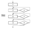
導通へ切り替えるこのフェーズのフローチャートが図2に例示される。 A flowchart of this phase of switching to continuity is illustrated in FIG.
このように、この図2を参照すると、導通へ切り替えるフェーズは、制御装置20が、導通命令を受信する初期ステップ101を有する。
Thus, referring to FIG. 2, the phase of switching to continuity has an
この場合、制御装置20は、ステップ110~135を行う。
In this case, the control device 20 performs
第1切り替えフェーズ110の間、制御装置20は、トランジスタ14のゲートGに、第1設定値Ic1に等しい強度を有する設定値電流の正の設定値電圧を加える。
During the
第1切り替えステップ110と平行に行われるステップ115の間、制御装置20は、モジュール16および18から測定値を受信し、これらの測定値を使用して、第1切り替えステップ110に対する停止条件を検証する。
During
特に、このステップ115の間、制御装置20は、下記の、
ゲートとエミッタとの間の電流の電圧VGEが、所定導通電圧閾値VONに到達する、
主電流Icの時間導関数dIc/dtが正になる、
第1切り替えステップ110の開始から経過した時間が、第1所定時間閾値T1に到達する、という停止条件の1つが満たされるまで、ステップ110を行い続ける。
In particular, during this
The voltage V GE of the current between the gate and the emitter reaches the predetermined conduction voltage threshold V ON ,
The time derivative dI c / dt of the main current I c becomes positive,
Step 110 is continued until one of the stop conditions that the time elapsed from the start of the
導通電圧閾値VONは、制御装置20により構成可能であり、方法100を行う前に、例えば、1Vと20Vとの間で調整可能である。この閾値VONは、好ましくは5Vに等しい。 The conduction voltage threshold V ON can be configured by the control device 20 and can be adjusted, for example, between 1V and 20V before performing the method 100. This threshold V ON is preferably equal to 5 V.
第1時間閾値T1は、制御装置20により構成可能であり、方法100を行う前に、例えば、1μsと8μsとの間で調整可能である。 The first time threshold T 1 is configurable by the control device 20 and can be adjusted, for example, between 1 μs and 8 μs before performing method 100.
第1設定値Ic1は、制御装置20により構成可能であり、方法100を行う前に、例えば、0.2Aと20Aとの間で調整可能である。 The first set value I c1 can be configured by the control device 20 and can be adjusted, for example, between 0.2A and 20A before performing the method 100.
そして、制御装置20は、トランジスタ14のゲートGに、第2設定値Ic2に等しい強度を有する設定値電流の正の設定値電圧を加える第2切り替えステップ120を行う。
Then, the control device 20 performs a
第2切り替えステップ120と平行に行われるステップ125の間、制御装置20は、モジュール18から測定値を受信し、これらの測定値を使用して、第2ステップ120に対する停止条件を検証する。
During
特に、このステップ125の間、制御装置20は、下記の、
主電流Icの時間導関数dIc/dtが負になる、
第2切り替えステップ120の開始から経過した時間が、第2所定時間閾値T2に到達する、という停止条件の1つが満たされるまで、ステップ120を行い続ける。
In particular, during this
The time derivative dI c / dt of the main current I c becomes negative,
Step 120 is continued until one of the stop conditions that the time elapsed from the start of the
第2時間閾値T2は、制御装置20により構成可能であり、方法100を行う前に、例えば、1μsと4μsとの間で調整可能である。 The second time threshold T 2 is configurable by the control device 20 and can be adjusted, for example, between 1 μs and 4 μs prior to performing method 100.
第2設定値Ic2は、制御装置20により構成可能であり、方法100を行う前に、例えば、0.2Aと20Aとの間で調整可能である。 The second set value I c2 can be configured by the control device 20 and can be adjusted, for example, between 0.2A and 20A before performing the method 100.
そして、制御装置20は、トランジスタ14のゲートGに、第3設定値Ic3に等しい強度を有する設定値電流の正の設定値電圧を加える第3切り替えステップ130を行う。
Then, the control device 20 performs a
第3切り替えステップ130と平行に行われるステップ135の間、制御装置20は、第3切り替えステップ130に対する停止条件を検証する。
During
特に、このステップ135の間、制御装置20は、第1切り替えステップ110の開始から経過した時間が、所定導通時間閾値TONに到達するまで、ステップ130を行い続ける。
In particular, during this
導通時間閾値TONは、制御装置20により構成可能であり、方法100を行う前に、例えば、3μsと20μsとの間で調整可能である。 The continuity time threshold T ON can be configured by the control device 20 and can be adjusted, for example, between 3 μs and 20 μs before performing the method 100.
第3設定値Ic3は、制御装置20により構成可能であり、方法100を行う前に、例えば、0.2Aと20Aとの間で調整可能である。 The third set value I c3 can be configured by the control device 20 and can be adjusted, for example, between 0.2A and 20A before performing the method 100.
そして、導通へ切り替えるフェーズの実現の間、各設定値Ic1~Ic3は、所定設定値のセットから選択されることを知ることができる。これらの値は、制御方法の実現の前に予め決められる。 Then, during the realization of the phase of switching to continuity, it can be known that each set value I c1 to I c3 is selected from a set of predetermined set values. These values are predetermined before the realization of the control method.
更に、設定値Ic1~Ic3は、互いに異なる。 Further, the set values I c1 to I c3 are different from each other.
記述された例において、設定値Ic1~Ic3は正であり、第3設定値Ic3は第1設定値Ic1より小さく、第2設定値Ic2より大きい。 In the described example, the set values I c1 to I c3 are positive, and the third set value I c3 is smaller than the first set value I c1 and larger than the second set value I c2 .
図3は、主電流Icと、ゲートGとエミッタEとの間の電圧VGEと、主電流Icの時間導関数dIc/dtと、ゲートGにおける設定値電流IGの動きと、を導通へ切り替えるフェーズのステップ110~130の実現の1つの例において例示する。 FIG. 3 shows the main current I c , the voltage V GE between the gate G and the emitter E, the time derivative dI c / dt of the main current I c , and the movement of the set value current IG at the gate G. Is illustrated in one example of the realization of steps 110-130 of the phase of switching to conduction.
非導通へ切り替えるフェーズは、導通フェーズと非導通フェーズとの間の遷移フェーズであり、特に、トランジスタ14をオン状態からオフ状態へ切り替えることを可能にする。
The phase for switching to non-conducting is a transition phase between the conducting phase and the non-conducting phase, and in particular, makes it possible to switch the
非導通へ切り替えるこのフェーズのフローチャートが図4に例示される。 A flowchart of this phase of switching to non-conduction is illustrated in FIG.
このように、この図4を参照すると、非導通へ切り替えるフェーズは、制御装置20が、非導通命令を受信する初期ステップ139を有する。
Thus, referring to FIG. 4, the phase of switching to non-conductivity has an
この場合、制御装置20は、ステップ140~165を行う。
In this case, the control device 20 performs
第4切り替えフェーズ140の間、制御装置20は、トランジスタ14のゲートGに、第4設定値Ic4に等しい強度を有する設定値電流の負の設定値電圧を加える。
During the
第4切り替えステップ140と平行に行われるステップ145の間、制御装置20は、モジュール16および18から測定値を受信し、これらの測定値を使用して、第4切り替えステップ140に対する停止条件を検証する。
During
特に、このステップ145の間、制御装置20は、下記の、
ゲートGとエミッタEとの間の電流の電圧VGEが、所定非導通電圧閾値VOFFに到達する、
主電流Icの時間導関数dIc/dtが負になる、
第4切り替えステップ140の開始から経過した時間が、第4所定時間閾値T4に到達する、という停止条件の1つが満たされるまで、ステップ140を行い続ける。
In particular, during this
The voltage V GE of the current between the gate G and the emitter E reaches a predetermined non-conducting voltage threshold V OFF .
The time derivative dI c / dt of the main current I c becomes negative,
Step 140 is continued until one of the stop conditions that the time elapsed from the start of the
非導通電圧閾値VOFFは、制御装置20により構成可能であり、方法100を行う前に、例えば、0.5Vと20Vとの間で調整可能である。この閾値VOFFは、好ましくは2Vに等しい。 The non-conducting voltage threshold V OFF can be configured by the control device 20 and can be adjusted, for example, between 0.5V and 20V before performing the method 100. This threshold V OFF is preferably equal to 2V.
第4時間閾値T4は、制御装置20により構成可能であり、方法100を行う前に、例えば、1μsと10μsとの間で調整可能である。 The fourth time threshold T 4 is configurable by the control device 20 and can be adjusted, for example, between 1 μs and 10 μs prior to performing method 100.
第4設定値Ic4の絶対値は、制御装置20により構成可能であり、方法100を行う前に、例えば、0.2Aと20Aとの間で調整可能である。 The absolute value of the fourth set value I c4 can be configured by the control device 20 and can be adjusted, for example, between 0.2A and 20A before performing the method 100.
そして、制御装置20は、トランジスタ14のゲートGに、第5設定値Ic5に等しい強度を有する設定値電流の負の設定値電圧を加える第5切り替えステップ150を行う。
Then, the control device 20 performs a
第5ステップ150と平行に行われるステップ155の間、制御装置20は、第5切り替えステップ150に対する停止条件を検証する。
During
特に、このステップ155の間、制御装置20は、第5切り替えステップ150の開始から経過した時間が、所定第5時間閾値T5に到達するまで、ステップ150を行い続ける。
In particular, during this
第5時間閾値T5は、制御装置20により構成可能であり、方法100を行う前に、例えば、0.5μsと2μsとの間で調整可能である。 The fifth time threshold T 5 is configurable by the control device 20 and can be adjusted, for example, between 0.5 μs and 2 μs prior to performing method 100.
第5設定値Ic5の絶対値は、制御装置20により構成可能であり、方法100を行う前に、例えば、0.2Aと20Aとの間で調整可能である。 The absolute value of the fifth set value I c5 can be configured by the control device 20 and can be adjusted, for example, between 0.2A and 20A before performing the method 100.
そして、制御装置20は、トランジスタ14のゲートGに、第6設定値Ic6に等しい強度を有する設定値電流の負の設定値電圧を加える第6切り替えステップ160を行う。
Then, the control device 20 performs a
第6切り替えステップ160と平行に行われるステップ165の間、制御装置20は、第6切り替えステップ160に対する停止条件を検証する。
During
特に、このステップ165の間、制御装置20は、第4切り替えステップ140の開始から経過した時間が、所定非導通時間閾値TOFFに到達するまで、ステップ160を行い続ける。
In particular, during this
非導通時間閾値TOFFは、制御装置20により構成可能であり、方法100を行う前に、例えば、3μsと20μsとの間で調整可能である。 The non-conduction time threshold T OFF can be configured by the control device 20 and can be adjusted, for example, between 3 μs and 20 μs before performing the method 100.
第6設定値Ic6の絶対値は、制御装置20により構成可能であり、方法100を行う前に、例えば、0.2Aと20Aとの間で調整可能である。 The absolute value of the sixth set value I c6 can be configured by the control device 20 and can be adjusted, for example, between 0.2A and 20A before performing the method 100.
そして、非導通へ切り替えるフェーズの実現の間、各設定値Ic4~Ic6は、所定設定値のセットから選択されることを知ることができる。これらの値は、制御方法100の実現の前に予め決められる。 Then, during the realization of the phase of switching to non-conduction, it can be known that each set value I c4 to I c6 is selected from a set of predetermined set values. These values are predetermined before the realization of the control method 100.
更に、設定値Ic4~Ic6は、互いに異なる。 Further, the set values I c4 to I c6 are different from each other.
記述された例において、設定値Ic4~Ic6は負であり、第6設定値Ic6は第5設定値Ic5より小さく、第4設定値Ic4より大きい。 In the described example, the set values I c4 to I c6 are negative, the sixth set value I c6 is smaller than the fifth set value I c5 , and larger than the fourth set value I c4 .
図5は、主電流Icと、ゲートGとエミッタEとの間の電圧VGEと、主電流Icの時間導関数dIc/dtと、ゲートGにおける設定値電流IGの動きと、を非導通へ切り替えるフェーズのステップ140~160の実現の1つの例において例示する。 FIG. 5 shows the main current I c , the voltage V GE between the gate G and the emitter E, the time derivative dI c / dt of the main current I c , and the movement of the set value current IG at the gate G. Is illustrated in one example of the realization of steps 140-160 of the phase of switching to non-conducting.
追加的に、導通へ切り替えるフェーズは、電気回路網10における短絡を検出するステップ170を有する。このステップ170は、ステップ110~135と平行に行われる。
Additionally, the phase of switching to continuity comprises
特に、この検出ステップ170は幾つかのサブステップを有しており、そのフローチャートが図6に例示される。
In particular, this
サブステップ171の間、制御装置20は、時間観測ウィンドウTobsにおける主電流Icの時間導関数dIc/dtの符号を観測する。
During
時間観測ウィンドウTobsの開始は、導通へ切り替えるフェーズの開始に対応する。 The start of the time observation window T obs corresponds to the start of the phase of switching to continuity.
所定テスト期間Ttの間、主電流Icの時間導関数dIc/dtが正の場合、制御装置20は、サブステップ172の間に、短絡の存在を検知する。そうでない場合は、制御装置20は、短絡は起き得ないと推測する。
If the time derivative dI c / dt of the main current I c is positive during the predetermined test period T t , the controller 20 detects the presence of a short circuit during
有利なように、ステップ170は、装置20が、検出された短絡の存在を確認するサブステップ173を更に有する。 Advantageously, step 170 further comprises a sub-step 173 in which device 20 confirms the presence of a detected short circuit.
特に、このサブステップ173の間、制御装置20は、主電流Icの時間導関数dIc/dtが、テスト期間Ttに係る追加期間の間、ゼロ以上に留まるときは、短絡の存在を確認する。そうでない場合は、制御装置20は、短絡は起きなかったと推測する。 In particular, during this sub-step 173, the controller 20 detects the presence of a short circuit when the time derivative dI c / dt of the main current I c stays above zero for an additional period of time with respect to the test period T t . confirm. If not, the controller 20 presumes that no short circuit has occurred.
追加期間は、テスト期間Ttの最後に開始し、例えば、時間観測ウィンドウTobsと共に終了する。 The additional period begins at the end of the test period T t and ends, for example, with the time observation window T obs .
短絡が検出されたときは、制御装置20は、該短絡を信号で通知し(signale)、トランジスタ14を、少なくとも所定非導通期間の間はオフ状態に保つ。
When a short circuit is detected, the controller 20 signals the short circuit and keeps the
テスト期間Ttは、制御装置20により構成可能であり、方法100を行う前に、例えば、1μsと10μsとの間で調整可能である。 The test period T t is configurable by the controller 20 and can be adjusted, for example, between 1 μs and 10 μs prior to performing method 100.
観測ウィンドウTobsの長さは、制御装置20により構成可能であり、方法100を行う前に、例えば、1μsと20μsとの間で調整可能である。 The length of the observation window T obs is configurable by the controller 20 and can be adjusted, for example, between 1 μs and 20 μs prior to performing method 100.
テスト期間Ttおよび追加期間は、観測ウィンドウTobsにおいて構成される。 The test period T t and the additional period are configured in the observation window T obs .
図7は、主電流Icと、主電流Icの時間導関数dIc/dtの動きと、を導通へ切り替えるフェーズの実現の2つの例において例示する。 FIG. 7 illustrates two examples of the realization of a phase in which the main current I c and the movement of the time derivative dI c / dt of the main current I c are switched to conduction.
曲線IcおよびIc/dtの実線に対応する第1例においては、短絡は起きなかった。この場合、導関数dIc/dtの符号は、テスト期間Ttの間に変化したので、制御装置20は、如何なる短絡をも検出しなかった。 No short circuit occurred in the first example corresponding to the solid lines of the curves I c and I c / dt. In this case, the sign of the derivative dI c / dt changed during the test period T t , so that the controller 20 did not detect any short circuit.
曲線IcおよびdIc/dtの破線に対応する第2例においては、短絡は起きた。この場合、導関数dIc/dtの符号は、テスト期間Ttの間、正であり、この期間外ではゼロに等しかった。従って、制御装置20は短絡を検出した。 In the second example corresponding to the dashed lines of the curves I c and dI c / dt, a short circuit occurred. In this case, the sign of the derivative dI c / dt was positive during the test period T t and was equal to zero outside this period. Therefore, the control device 20 has detected a short circuit.
本発明が、いくつかの利点を有することを知ることができる。 It can be seen that the present invention has several advantages.
本発明に係る制御方法は、ゲートGとエミッタEとの間の電圧VGEの測定値と、主電流Icの導関数dIc/dtの符号のみを使用して、オフ状態とオン状態との間のトランジスタの切り替えの間の異なる中間ステップを制御する。 The control method according to the present invention uses only the measured value of the voltage V GE between the gate G and the emitter E and the sign of the derivative dI c / dt of the main current I c to be in the off state and the on state. Controls different intermediate steps between switching transistors between.
主電流Icの値、または主電流Icの導関数dIc/dtの値の測定値は、方法を行うために必要でないことに留意すべきである。このように、導関数dIc/dtの符号のみがトランジスタを制御するために重要であり、電気回路網における種々の測定手段に対する必要条件を簡素にすることを可能にする。 It should be noted that the measured value of the main current I c , or the derivative dI c / dt of the main current I c , is not necessary to carry out the method. Thus, only the sign of the derivative dI c / dt is important for controlling the transistor, making it possible to simplify the requirements for various measuring means in the electrical network.
そしてこれは、トランジスタを組み込んだ電気回路の構造を相当に簡素にする。 And this considerably simplifies the structure of the electric circuit incorporating the transistor.
更に、主電流Icの導関数dIc/dtの符号は、電力構成要素を非導通にするときの過電圧を制限する調整手段として使用される。 Further, the sign of the derivative dI c / dt of the main current I c is used as an adjusting means for limiting the overvoltage when the power component is made non-conducting.
このため、非導通中の過電圧を制限するために、インバータフィードバック回路、特に、電力構成要素の端子間の電圧に接続される回路は必要でない。そして、これは、本発明の特別な利点を構成する。 Therefore, in order to limit the overvoltage during non-conduction, an inverter feedback circuit, particularly a circuit connected to the voltage between the terminals of the power component, is not required. And this constitutes a special advantage of the present invention.
Claims (10)
前記方法(100)は、前記オン状態と前記オフ状態との間の切り替えフェーズを有し、前記フェーズは、設定値電流を生成することを有し、前記トランジスタ(14)の前記ゲート上の前記設定値電流の強度は、異なる設定値(Ic1、...、Ic6)を取り、前記設定値(Ic1、...、Ic6)の少なくとも幾つかは、前記主電流(Ic)の時間導関数(dIc/dt)の符号によって選択され、各設定値(Ic1、...、Ic6)は、所定設定値(Ic1、...、Ic6)のセットから選択される、方法(100)。 A method (100) for controlling an IGBT type transistor (14), wherein the transistor (14) has a gate (G), a collector (C), and an emitter (E), and has a main current ( Ic ). An on state that flows between the collector (C) and the emitter (E) and an off state in which the collector (C) is electrically isolated from the emitter (E) are defined.
The method (100) has a switching phase between the on state and the off state, the phase having to generate a set value current, on the gate of the transistor (14). The intensity of the set value current takes different set values (I c1 , ..., I c6 ), and at least some of the set values (I c1 , ..., I c6 ) are the main current (I c6). Selected by the sign of the time derivative (dI c / dt) of c ), each set value (I c1 , ..., I c6 ) is a set of predetermined set values (I c1 , ..., I c6 ). Method (100) selected from.
前記ゲート(G)と前記エミッタ(E)との間の電圧(VGE)を測定することと、
前記電圧を、少なくとも1つの所定電圧閾値(VON、VOFF)と比較することと、を更に有する、請求項1に記載の方法(100)。 The switching phase is
Measuring the voltage (V GE ) between the gate (G) and the emitter (E)
The method (100) of claim 1, further comprising comparing the voltage with at least one predetermined voltage threshold (V ON , V OFF ).
前記トランジスタ(14)を、前記オフ状態から前記オン状態に切り替える命令を受信することを有する初期導通ステップ(101)と、
前記ゲート(G)と前記エミッタ(E)との間の電圧(VGE)が、所定導通電圧閾値(VON)に到達するまで、または、前記主電流(Ic)の前記時間導関数(dIc/dt)が正になるまで、または、第1切り替えステップ(110)の開始から経過した時間が、第1所定時間閾値(T1)に到達するまで、第1設定値(Ic1)に等しい強度の前記設定値電流(Ic1)を生成することを有する前記第1切り替えステップ(110)と、
前記主電流(Ic)の前記時間導関数(dIc/dt)が負になるまで、または、第2切り替えステップ(120)の開始から経過した時間が、第2所定時間閾値(T2)に到達するまで、第2設定値(Ic2)に等しい強度の前記設定値電流を生成することを有する前記第2切り替えステップ(120)と、
前記第1切り替えステップ(110)の開始から経過した時間が、所定導通時間閾値(TON)に到達するまで、第3設定値(Ic3)に等しい強度の前記設定値電流を生成することを有する第3切り替えステップ(130)と、を有する、請求項5に記載の方法(100)。 The phase of switching to continuity is continuously performed in the following,
An initial conduction step (101) comprising receiving an instruction to switch the transistor (14) from the off state to the on state.
Until the voltage (V GE ) between the gate (G) and the emitter (E) reaches a predetermined conduction voltage threshold (V ON ), or the time derivative of the main current (I c ). The first set value (I c1 ) until (dI c / dt) becomes positive or until the time elapsed from the start of the first switching step (110) reaches the first predetermined time threshold (T 1 ). The first switching step (110), which comprises generating the set value current (I c1 ) of intensity equal to).
The time until the time derivative (dI c / dt) of the main current (I c ) becomes negative or the time elapsed from the start of the second switching step (120) is the second predetermined time threshold value (T 2 ). The second switching step (120), which has the effect of generating the set value current of intensity equal to the second set value (I c2 ), until reaching.
It is determined that the set value current having an intensity equal to the third set value (I c3 ) is generated until the time elapsed from the start of the first switching step (110) reaches the predetermined conduction time threshold value (T ON ). The method (100) according to claim 5, further comprising a third switching step (130).
前記トランジスタを前記オン状態から前記オフ状態に切り替える命令を受信することを有する初期非導通ステップ(139)と、
前記ゲート(G)と前記エミッタ(E)との間の電流の電圧(VGE)が、所定非導通電圧閾値(VOFF)に到達するまで、または、前記主電流(Ic)の前記時間導関数(dIc/dt)が負になるまで、または、第4切り替えステップ(140)の開始から経過した時間が、第4所定時間閾値(T4)に到達するまで、第4設定値(Ic4)に等しい強度の前記設定値電流を生成することを有する前記第4切り替えステップ(140)と、
第5切り替えステップ(150)の開始から経過した時間が、第5所定時間閾値(T5)に到達するまで、第5設定値(Ic5)に等しい強度の前記設定値電流を生成することを有する前記第5切り替えステップと、
前記第4切り替えステップ(140)の開始から経過した時間が、所定非導通時間閾値(TOFF)に到達するまで、第6設定値(Ic6)に等しい強度の前記設定値電流を生成することを有する第6切り替えステップ(160)と、を有する、請求項5または6に記載の方法(100)。 The phase of switching to non-conduction is continuously performed in the following,
An initial non-conducting step (139) comprising receiving an instruction to switch the transistor from the on state to the off state.
Until the voltage (V GE ) of the current between the gate (G) and the emitter (E) reaches a predetermined non-conducting voltage threshold (V OFF ), or the time of the main current (I c ). The fourth set value (until the derivative (dI c / dt) becomes negative, or the time elapsed from the start of the fourth switching step (140) reaches the fourth predetermined time threshold (T 4 ). The fourth switching step (140), which comprises generating the set value current of intensity equal to I c4 ), and
It is determined that the set value current having an intensity equal to the fifth set value (I c5 ) is generated until the time elapsed from the start of the fifth switching step (150) reaches the fifth predetermined time threshold value (T 5 ). With the fifth switching step having
The set value current having an intensity equal to the sixth set value (I c6 ) is generated until the time elapsed from the start of the fourth switching step (140) reaches the predetermined non-conduction time threshold value (T OFF ). The method (100) according to claim 5 or 6, further comprising a sixth switching step (160).
前記装置は、設定値電流を生成することができ、前記トランジスタ(14)の前記ゲート上の前記設定値電流の強度は、異なる設定値(Ic1、...、Ic6)を取り、前記設定値(Ic1、...、Ic6)の少なくとも幾つかは、前記主電流(Ic)の時間導関数(dIc/dt)の符号によって選択され、各設定値(Ic1、...、Ic6)は、所定設定値(Ic1、...、Ic6)のセットから選択される、制御装置(20)。 The control device (20) of the IGBT type transistor (14), wherein the transistor (14) has a gate (G), a collector (C), and an emitter (E), and the main current ( Ic ) is the said. An on state that flows between the collector (C) and the emitter (E) and an off state in which the collector (C) is electrically isolated from the emitter (E) are defined.
The apparatus can generate a set value current, and the intensity of the set value current on the gate of the transistor (14) takes different set values (I c1 , ..., I c6 ). At least some of the set values (I c1 , ..., I c6 ) are selected by the sign of the time derivative (dI c / dt) of the main current (I c ), and each set value (I c1 , I c1). ..., I c6 ) is a control device (20) selected from a set of predetermined set values (I c1 , ..., I c6 ).
Applications Claiming Priority (2)
| Application Number | Priority Date | Filing Date | Title |
|---|---|---|---|
| FR1658986 | 2016-09-23 | ||
| FR1658986A FR3056859B1 (en) | 2016-09-23 | 2016-09-23 | METHOD FOR CONTROLLING AN IGBT TYPE TRANSISTOR AND STEERING DEVICE THEREFOR |
Publications (2)
| Publication Number | Publication Date |
|---|---|
| JP2018050297A JP2018050297A (en) | 2018-03-29 |
| JP7071079B2 true JP7071079B2 (en) | 2022-05-18 |
Family
ID=57860978
Family Applications (1)
| Application Number | Title | Priority Date | Filing Date |
|---|---|---|---|
| JP2017182123A Active JP7071079B2 (en) | 2016-09-23 | 2017-09-22 | Control method of IGBT type transistor and related control device |
Country Status (7)
| Country | Link |
|---|---|
| US (1) | US10319822B2 (en) |
| EP (1) | EP3300253B1 (en) |
| JP (1) | JP7071079B2 (en) |
| CN (1) | CN107872211B (en) |
| ES (1) | ES2754698T3 (en) |
| FR (1) | FR3056859B1 (en) |
| PL (1) | PL3300253T3 (en) |
Families Citing this family (2)
| Publication number | Priority date | Publication date | Assignee | Title |
|---|---|---|---|---|
| KR102229656B1 (en) | 2019-11-27 | 2021-03-19 | 현대모비스 주식회사 | Apparatus for controlling operating speed of power semiconductor device and power semiconductor system |
| KR102460421B1 (en) | 2020-12-04 | 2022-10-31 | 현대모비스 주식회사 | Apparatus and method for monitoring current of power semiconductor device |
Citations (2)
| Publication number | Priority date | Publication date | Assignee | Title |
|---|---|---|---|---|
| JP2002524010A (en) | 1998-08-12 | 2002-07-30 | ダイムラークライスラー・アクチェンゲゼルシャフト | Apparatus for controlling voltage-charge control power semiconductor device |
| JP2015525034A (en) | 2012-07-13 | 2015-08-27 | ヴァレオ システム ドゥ コントロール モトゥール | Device for controlling at least one transistor |
Family Cites Families (14)
| Publication number | Priority date | Publication date | Assignee | Title |
|---|---|---|---|---|
| DE19610895A1 (en) * | 1996-03-20 | 1997-09-25 | Abb Research Ltd | Method for switching on an IGBT and device for carrying out the method |
| EP0926826A1 (en) * | 1997-12-18 | 1999-06-30 | ABB Research Ltd. | Method and device in power transistor |
| US6060943A (en) * | 1998-04-14 | 2000-05-09 | Nmb (Usa) Inc. | Circuit simulating a diode |
| GB2417149A (en) * | 2004-08-12 | 2006-02-15 | Bombardier Transp Gmbh | Digital adaptive control of IGBT or MOS gate charging current in a converter for a railway traction motor |
| US8829949B2 (en) * | 2012-01-17 | 2014-09-09 | Franc Zajc | Method and apparatus for driving a voltage controlled power switch device |
| DE102012207147B4 (en) * | 2012-04-27 | 2016-01-21 | Infineon Technologies Ag | Method for driving power semiconductor switches |
| JP6140814B2 (en) * | 2012-05-14 | 2017-05-31 | テュフ ラインランド(シャンハイ)カンパニー リミテッド | Photovoltaic element evaluation method, measurement system configuration, and method of using the measurement system configuration |
| DE102012011755A1 (en) * | 2012-06-12 | 2013-12-12 | Tridonic Gmbh & Co. Kg | Power factor correction circuit, lighting device and method of controlling a power factor correction circuit |
| CN102969889B (en) * | 2012-11-05 | 2015-08-12 | 矽力杰半导体技术(杭州)有限公司 | A self-powered source drive circuit and switching power supply using it |
| JP6333358B2 (en) * | 2013-04-05 | 2018-05-30 | エービービー テクノロジー エルティーディー. | RC-IGBT switching pulse control |
| JP5907199B2 (en) * | 2014-03-12 | 2016-04-26 | トヨタ自動車株式会社 | Semiconductor device and method for controlling semiconductor device |
| JP2016073052A (en) * | 2014-09-29 | 2016-05-09 | アイシン・エィ・ダブリュ株式会社 | Switching controller |
| EP3138692A1 (en) * | 2015-08-06 | 2017-03-08 | OCE-Technologies B.V. | Imaging system for processing a media |
| FR3056756B1 (en) * | 2016-09-23 | 2020-06-12 | Alstom Transport Technologies | METHOD FOR DETECTING A SHORT-CIRCUIT IN AN ELECTRIC CIRCUIT COMPRISING AN IGBT-TYPE TRANSISTOR AND ASSOCIATED DRIVING DEVICE |
-
2016
- 2016-09-23 FR FR1658986A patent/FR3056859B1/en not_active Expired - Fee Related
-
2017
- 2017-09-22 ES ES17192721T patent/ES2754698T3/en active Active
- 2017-09-22 US US15/712,665 patent/US10319822B2/en active Active
- 2017-09-22 JP JP2017182123A patent/JP7071079B2/en active Active
- 2017-09-22 EP EP17192721.3A patent/EP3300253B1/en active Active
- 2017-09-22 PL PL17192721T patent/PL3300253T3/en unknown
- 2017-09-25 CN CN201710879626.8A patent/CN107872211B/en active Active
Patent Citations (2)
| Publication number | Priority date | Publication date | Assignee | Title |
|---|---|---|---|---|
| JP2002524010A (en) | 1998-08-12 | 2002-07-30 | ダイムラークライスラー・アクチェンゲゼルシャフト | Apparatus for controlling voltage-charge control power semiconductor device |
| JP2015525034A (en) | 2012-07-13 | 2015-08-27 | ヴァレオ システム ドゥ コントロール モトゥール | Device for controlling at least one transistor |
Also Published As
| Publication number | Publication date |
|---|---|
| FR3056859B1 (en) | 2018-11-30 |
| EP3300253B1 (en) | 2019-08-14 |
| JP2018050297A (en) | 2018-03-29 |
| ES2754698T3 (en) | 2020-04-20 |
| CN107872211B (en) | 2023-04-07 |
| PL3300253T3 (en) | 2020-03-31 |
| EP3300253A1 (en) | 2018-03-28 |
| US10319822B2 (en) | 2019-06-11 |
| US20180090578A1 (en) | 2018-03-29 |
| CN107872211A (en) | 2018-04-03 |
| FR3056859A1 (en) | 2018-03-30 |
Similar Documents
| Publication | Publication Date | Title |
|---|---|---|
| CN109596960B (en) | Evaluating gate-source leakage current in transistor devices | |
| US9455569B2 (en) | Procedures for the operation of an electrical circuit | |
| JP5832578B2 (en) | Motor drive device having failure detection function of motor insulation resistance deterioration detection unit and failure detection method | |
| CN105007023A (en) | Motor drive apparatus | |
| US10727729B2 (en) | Power converter | |
| US9964599B2 (en) | Diagnostic system for a DC-DC voltage converter | |
| JP6415566B2 (en) | Voltage detector | |
| CN105324675B (en) | device and method for monitoring power semiconductor switch | |
| JP7071079B2 (en) | Control method of IGBT type transistor and related control device | |
| US10135234B2 (en) | Preventive apparatus | |
| JP6954013B2 (en) | Judgment device | |
| JP5748610B2 (en) | Charger | |
| JP7020834B2 (en) | Short circuit detection methods and related controls in electrical networks with IGBT transistors | |
| JP6102672B2 (en) | Insulation state determination device and insulation state determination method | |
| CN107957550B (en) | Identification of faults in a generator unit | |
| EP3361270B1 (en) | Method and device for fast insulation monitoring of electrical devices having large ground capacitance | |
| CN105425892A (en) | Current control circuit | |
| CN102656473A (en) | Method and apparatus for calibrating voltage measuring devices on drive circuits | |
| US11099225B2 (en) | Method for determining the output voltage of a transistor | |
| US20250202247A1 (en) | Switching circuit for cell balancing in a battery management system | |
| JP2014143049A (en) | Excitation rush current suppression device | |
| JP2010071809A (en) | Method of inspecting electric characteristic of semiconductor device | |
| JP2019086306A (en) | Testing device of semiconductor device | |
| US20210050720A1 (en) | Operation device and operation system | |
| CN119231894A (en) | A controller and a control method |
Legal Events
| Date | Code | Title | Description |
|---|---|---|---|
| A621 | Written request for application examination |
Free format text: JAPANESE INTERMEDIATE CODE: A621 Effective date: 20200821 |
|
| A977 | Report on retrieval |
Free format text: JAPANESE INTERMEDIATE CODE: A971007 Effective date: 20210810 |
|
| A131 | Notification of reasons for refusal |
Free format text: JAPANESE INTERMEDIATE CODE: A131 Effective date: 20210824 |
|
| A521 | Request for written amendment filed |
Free format text: JAPANESE INTERMEDIATE CODE: A523 Effective date: 20211101 |
|
| TRDD | Decision of grant or rejection written | ||
| A01 | Written decision to grant a patent or to grant a registration (utility model) |
Free format text: JAPANESE INTERMEDIATE CODE: A01 Effective date: 20220405 |
|
| A61 | First payment of annual fees (during grant procedure) |
Free format text: JAPANESE INTERMEDIATE CODE: A61 Effective date: 20220506 |
|
| R150 | Certificate of patent or registration of utility model |
Ref document number: 7071079 Country of ref document: JP Free format text: JAPANESE INTERMEDIATE CODE: R150 |
|
| R250 | Receipt of annual fees |
Free format text: JAPANESE INTERMEDIATE CODE: R250 |