JP7123692B2 - 配線基板設計支援装置、配線基板ビア配置方法及び配線基板ビア配置プログラム - Google Patents
配線基板設計支援装置、配線基板ビア配置方法及び配線基板ビア配置プログラム Download PDFInfo
- Publication number
- JP7123692B2 JP7123692B2 JP2018152509A JP2018152509A JP7123692B2 JP 7123692 B2 JP7123692 B2 JP 7123692B2 JP 2018152509 A JP2018152509 A JP 2018152509A JP 2018152509 A JP2018152509 A JP 2018152509A JP 7123692 B2 JP7123692 B2 JP 7123692B2
- Authority
- JP
- Japan
- Prior art keywords
- wiring board
- wiring
- vias
- movement
- vertical
- Prior art date
- Legal status (The legal status is an assumption and is not a legal conclusion. Google has not performed a legal analysis and makes no representation as to the accuracy of the status listed.)
- Active
Links
Images




Classifications
-
- G—PHYSICS
- G06—COMPUTING OR CALCULATING; COUNTING
- G06F—ELECTRIC DIGITAL DATA PROCESSING
- G06F30/00—Computer-aided design [CAD]
- G06F30/30—Circuit design
- G06F30/39—Circuit design at the physical level
- G06F30/394—Routing
-
- G—PHYSICS
- G01—MEASURING; TESTING
- G01R—MEASURING ELECTRIC VARIABLES; MEASURING MAGNETIC VARIABLES
- G01R1/00—Details of instruments or arrangements of the types included in groups G01R5/00 - G01R13/00 and G01R31/00
- G01R1/02—General constructional details
- G01R1/06—Measuring leads; Measuring probes
- G01R1/067—Measuring probes
- G01R1/073—Multiple probes
- G01R1/07307—Multiple probes with individual probe elements, e.g. needles, cantilever beams or bump contacts, fixed in relation to each other, e.g. bed of nails fixture or probe card
- G01R1/07342—Multiple probes with individual probe elements, e.g. needles, cantilever beams or bump contacts, fixed in relation to each other, e.g. bed of nails fixture or probe card the body of the probe being at an angle other than perpendicular to test object, e.g. probe card
-
- G—PHYSICS
- G01—MEASURING; TESTING
- G01R—MEASURING ELECTRIC VARIABLES; MEASURING MAGNETIC VARIABLES
- G01R3/00—Apparatus or processes specially adapted for the manufacture or maintenance of measuring instruments, e.g. of probe tips
-
- H—ELECTRICITY
- H05—ELECTRIC TECHNIQUES NOT OTHERWISE PROVIDED FOR
- H05K—PRINTED CIRCUITS; CASINGS OR CONSTRUCTIONAL DETAILS OF ELECTRIC APPARATUS; MANUFACTURE OF ASSEMBLAGES OF ELECTRICAL COMPONENTS
- H05K3/00—Apparatus or processes for manufacturing printed circuits
- H05K3/40—Forming printed elements for providing electric connections to or between printed circuits
- H05K3/4038—Through-connections; Vertical interconnect access [VIA] connections
-
- G—PHYSICS
- G01—MEASURING; TESTING
- G01R—MEASURING ELECTRIC VARIABLES; MEASURING MAGNETIC VARIABLES
- G01R1/00—Details of instruments or arrangements of the types included in groups G01R5/00 - G01R13/00 and G01R31/00
- G01R1/02—General constructional details
- G01R1/06—Measuring leads; Measuring probes
- G01R1/067—Measuring probes
- G01R1/073—Multiple probes
- G01R1/07307—Multiple probes with individual probe elements, e.g. needles, cantilever beams or bump contacts, fixed in relation to each other, e.g. bed of nails fixture or probe card
-
- G—PHYSICS
- G06—COMPUTING OR CALCULATING; COUNTING
- G06F—ELECTRIC DIGITAL DATA PROCESSING
- G06F30/00—Computer-aided design [CAD]
- G06F30/30—Circuit design
- G06F30/39—Circuit design at the physical level
Landscapes
- Engineering & Computer Science (AREA)
- Physics & Mathematics (AREA)
- General Physics & Mathematics (AREA)
- Theoretical Computer Science (AREA)
- Computer Hardware Design (AREA)
- Evolutionary Computation (AREA)
- Geometry (AREA)
- General Engineering & Computer Science (AREA)
- Manufacturing & Machinery (AREA)
- Microelectronics & Electronic Packaging (AREA)
- Computer Networks & Wireless Communication (AREA)
- Production Of Multi-Layered Print Wiring Board (AREA)
- Design And Manufacture Of Integrated Circuits (AREA)
Description
以下では、本発明に係る配線基板設計支援装置、配線基板ビア配置方法及び配線基板ビア配置プログラムの実施形態を、図面を参照しながら詳細に説明する。
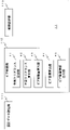
図2は、この実施形態に係る配線基板設計支援装置のハードウェア構成を示す構成図である。
次に、この実施形態に係る配線基板設計支援装置10における配線基板ビア配置処理の動作を、図面を参照しながら詳細に説明する。
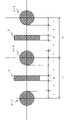
ここで、配線数nとする場合の余剰クリアランスmの算出方法について、図5及び図6を参照しながら説明する。
m=p-min p
=p-2r-(n×w)-(n+1)c …(1)
次に、配線数(n+1)とする場合の不足クリアランスsの算出方法について、図7を参照しながら説明する。
s=min p-p
=2r+(n+1)w+(n+2)-p …(2)
主制御部11は、余剰クリアランスmの値と不足クリアランスsの値とを比較する(S13)。
S13において、余剰クリアランスmの値が不足クリアランスsの値以上である場合、主制御部11は、等ピッチの格子状に配置されている各ビアパッドの位置座標から、X方向及びY方向に移動させるための移動量deltaを算出する(S14)。
s/2≦ delta ≦m/2 …(3)
主制御部11は、不等ピッチで各ビアパッド2が配置されると、ビアパッド2の間に配線3を設定する。
以上のように、この実施形態によれば、等ピッチで格子状に配置されたビアパッドの位置座標にオフセット量としての移動量を加算又は減算して、不等ピッチのビアパッドを配置しているので、ビア配置領域を拡大させずに、縦方向、横方向共に、偏りなく配線収容性を向上させることができる。
上述した実施形態においても種々の変形実施形態を言及したが、本発明は、以下の変形実施形態にも適用することができる。
10…配線基板設計支援装置、11…主制御部、12…外部記憶部、13…表示部、14…入力部、11P…配線基板ビア配置プログラム、111…設計データ読込部、112…ビア配置部、113…配線設定部、41…余剰クリアランス算出部、42…不足クリアランス算出部、43…ビア移動量算出部、44…ビア座標算出部、45…ビア配置情報出力部。
Claims (5)
- 配線基板に複数のビアを配置する配線基板設計支援装置において、
上記配線基板に配置させるビア及び配線に関する設計情報を記憶する設計情報記憶手段と、
上記設計情報に基づいて、縦横の間隔を等間隔とした格子点の位置を、縦方向及び横方向に所定の移動量だけ移動させるものであって、当該格子の行毎に上記格子点の横の移動方向を交互に変え、かつ、当該格子の列毎に上記格子点の縦の移動方向を交互に変えて、移動後の上記格子点の位置にビアを配置する配線基板ビア配置手段と
を備えることを特徴とする配線基板設計支援装置。 - 上記配線基板ビア配置手段が、
上記設計情報に基づいて、上記縦横の間隔が等間隔とした格子点の位置にビアを配置して、ビア間に配線を配置したときの余剰クリアランスの値を求める余剰クリアランス算出部と、
上記ビア間に、上記配線の数を増やして上記配線を配置したとき不足クリアランスの値を求める不足クリアランス算出部と、
上記余剰クリアランスの値と上記不足クリアランスの値との比較結果に応じて、上記格子点の位置を縦方向及び横方向に移動させる移動量を算出する移動量算出部と
を有することを特徴とする請求項1に記載の配線基板設計支援装置。 - 上記配線基板ビア配置手段により配置されたビア配列においてビア間に配線を設定する配線設定手段を備えることを特徴とする請求項1又は2に記載の配線基板設計支援装置。
- 配線基板に複数のビアを配置する配線基板ビア配置方法において、
設計情報記憶手段が、上記配線基板に配置させるビア及び配線に関する設計情報を記憶し、
配線基板ビア配置手段が、上記設計情報に基づいて、縦横の間隔を等間隔とした格子点の位置を、縦方向及び横方向に所定の移動量だけ移動させるものであって、当該格子の行毎に上記格子点の横の移動方向を交互に変え、かつ、当該格子の列毎に上記格子点の縦の移動方向を交互に変えて、移動後の上記格子点の位置にビアを配置する
ことを特徴とする配線基板ビア配置方法。 - 配線基板に複数のビアを配置する配線基板ビア配置プログラムにおいて、
上記配線基板に配置させるビア及び配線に関する設計情報を記憶する設計情報記憶手段を有するコンピュータを、
上記設計情報に基づいて、縦横の間隔を等間隔とした格子点の位置を、縦方向及び横方向に所定の移動量だけ移動させるものであって、当該格子の行毎に上記格子点の横の移動方向を交互に変え、かつ、当該格子の列毎に上記格子点の縦の移動方向を交互に変えて、移動後の上記格子点の位置にビアを配置する配線基板ビア配置手段
として機能させることを特徴とする配線基板ビア配置プログラム。
Priority Applications (5)
| Application Number | Priority Date | Filing Date | Title |
|---|---|---|---|
| JP2018152509A JP7123692B2 (ja) | 2018-08-13 | 2018-08-13 | 配線基板設計支援装置、配線基板ビア配置方法及び配線基板ビア配置プログラム |
| US16/454,441 US10776556B2 (en) | 2018-08-13 | 2019-06-27 | Wiring board design support apparatus, method for wiring board via arrangement and storage medium recording program for wiring board via arrangement |
| TW108123535A TWI724447B (zh) | 2018-08-13 | 2019-07-04 | 配線基板設計支援裝置,配線基板通孔配置方法及配線基板通孔配置程式 |
| KR1020190085240A KR102289322B1 (ko) | 2018-08-13 | 2019-07-15 | 배선기판 설계 지원장치, 배선기판 비아 배치방법 및 배선기판 비아 배치 프로그램 |
| CN201910744180.7A CN110874518B (zh) | 2018-08-13 | 2019-08-13 | 布线基板的设计辅助装置、导孔配置方法以及记录介质 |
Applications Claiming Priority (1)
| Application Number | Priority Date | Filing Date | Title |
|---|---|---|---|
| JP2018152509A JP7123692B2 (ja) | 2018-08-13 | 2018-08-13 | 配線基板設計支援装置、配線基板ビア配置方法及び配線基板ビア配置プログラム |
Publications (2)
| Publication Number | Publication Date |
|---|---|
| JP2020027487A JP2020027487A (ja) | 2020-02-20 |
| JP7123692B2 true JP7123692B2 (ja) | 2022-08-23 |
Family
ID=69406146
Family Applications (1)
| Application Number | Title | Priority Date | Filing Date |
|---|---|---|---|
| JP2018152509A Active JP7123692B2 (ja) | 2018-08-13 | 2018-08-13 | 配線基板設計支援装置、配線基板ビア配置方法及び配線基板ビア配置プログラム |
Country Status (5)
| Country | Link |
|---|---|
| US (1) | US10776556B2 (ja) |
| JP (1) | JP7123692B2 (ja) |
| KR (1) | KR102289322B1 (ja) |
| CN (1) | CN110874518B (ja) |
| TW (1) | TWI724447B (ja) |
Families Citing this family (4)
| Publication number | Priority date | Publication date | Assignee | Title |
|---|---|---|---|---|
| US11901286B2 (en) * | 2021-01-28 | 2024-02-13 | Taiwan Semiconductor Manufacturing Company, Ltd. | Diagonal via pattern and method |
| CN112949244B (zh) * | 2021-03-29 | 2022-12-13 | 福建福强精密印制线路板有限公司 | 智能选钉方法及存储介质 |
| CN114340175A (zh) * | 2022-01-10 | 2022-04-12 | 鹤山市泰利诺电子有限公司 | 电路板锣板方法 |
| CN117320268A (zh) * | 2022-06-21 | 2023-12-29 | 中兴智能科技南京有限公司 | 电路板、电路板组件 |
Citations (3)
| Publication number | Priority date | Publication date | Assignee | Title |
|---|---|---|---|---|
| JP2002334124A (ja) | 2001-05-11 | 2002-11-22 | Nec Corp | プリント配線板における配線幅調整装置及び配線幅調整方法 |
| US7269813B2 (en) | 2004-11-19 | 2007-09-11 | Alcatel | Off-width pitch for improved circuit card routing |
| WO2009122494A1 (ja) | 2008-03-31 | 2009-10-08 | 富士通株式会社 | 配線基板設計支援装置、配線基板設計支援方法、配線基板設計支援プログラムおよび同プログラムを記録したコンピュータ読取可能な記録媒体 |
Family Cites Families (29)
| Publication number | Priority date | Publication date | Assignee | Title |
|---|---|---|---|---|
| JPH06140751A (ja) * | 1992-10-28 | 1994-05-20 | Matsushita Electric Works Ltd | プリント配線基板へのリード線半田付け方法 |
| US6510539B1 (en) * | 1999-10-29 | 2003-01-21 | International Business Machines Corporation | System and method for physically modeling electronic modules wiring |
| JP3786398B2 (ja) * | 2000-09-07 | 2006-06-14 | 新光電気工業株式会社 | 半導体パッケージの配線方法 |
| US6762366B1 (en) * | 2001-04-27 | 2004-07-13 | Lsi Logic Corporation | Ball assignment for ball grid array package |
| US8575954B2 (en) * | 2002-06-24 | 2013-11-05 | Advantest (Singapore) Pte Ltd | Structures and processes for fabrication of probe card assemblies with multi-layer interconnect |
| US7624367B2 (en) * | 2002-11-18 | 2009-11-24 | Cadence Design Systems, Inc. | Method and system for routing |
| US7007258B2 (en) * | 2003-06-13 | 2006-02-28 | Sun Microsystems, Inc. | Method, apparatus, and computer program product for generation of a via array within a fill area of a design layout |
| US7738259B2 (en) * | 2004-01-22 | 2010-06-15 | Alcatel Lucent | Shared via decoupling for area arrays components |
| JP4528024B2 (ja) * | 2004-04-28 | 2010-08-18 | 富士通株式会社 | 回路解析方法を実行させるためのプログラム |
| US7340711B2 (en) * | 2004-06-04 | 2008-03-04 | Cadence Design Systems, Inc. | Method and apparatus for local preferred direction routing |
| US7323787B2 (en) * | 2005-01-25 | 2008-01-29 | Alcatel | Off-grid decoupling of ball grid array (BGA) devices and method |
| JP2007041867A (ja) * | 2005-08-03 | 2007-02-15 | Elpida Memory Inc | インダクタンス解析システムと方法並びにプログラム |
| US7368667B2 (en) * | 2005-08-10 | 2008-05-06 | Alcatel | Using rows/columns of micro-vias to create PCB routing channels in BGA interconnect grid (micro-via channels) |
| JP4270210B2 (ja) | 2006-01-20 | 2009-05-27 | セイコーエプソン株式会社 | 回路基板、バンプ付き半導体素子の実装構造、及び電気光学装置、並びに電子機器 |
| US7464358B1 (en) * | 2006-01-26 | 2008-12-09 | Cadence Design Systems, Inc. | Method for resolving overloads in autorouting physical interconnections |
| TWI319298B (en) * | 2007-03-19 | 2010-01-01 | Inventec Corp | Via-adjusting method and system |
| US7797663B2 (en) * | 2007-04-04 | 2010-09-14 | Cisco Technology, Inc. | Conductive dome probes for measuring system level multi-GHZ signals |
| TWI330798B (en) * | 2007-05-01 | 2010-09-21 | Inventec Corp | Method for designing printed circuit board |
| JP5223790B2 (ja) * | 2009-06-22 | 2013-06-26 | 富士通株式会社 | プリント回路板設計支援プログラム、プリント回路板設計支援方法、およびプリント回路板設計支援装置 |
| JP5212296B2 (ja) * | 2009-07-22 | 2013-06-19 | 富士通株式会社 | 配線設計支援装置、配線設計支援方法、及び配線設計支援プログラム |
| JP5459543B2 (ja) * | 2009-12-04 | 2014-04-02 | 日本電気株式会社 | 回路基板及びその設計方法 |
| JP2012038043A (ja) * | 2010-08-05 | 2012-02-23 | Sharp Corp | 配線設計支援装置、配線設計支援方法、および配線設計支援プログラム |
| US9627306B2 (en) * | 2012-02-15 | 2017-04-18 | Cypress Semiconductor Corporation | Ball grid structure |
| JP5779145B2 (ja) * | 2012-06-28 | 2015-09-16 | 株式会社Screenホールディングス | 配線データの生成装置、生成方法、そのプログラム、および描画装置 |
| CN104982092B (zh) * | 2013-02-07 | 2017-04-05 | 松下知识产权经营株式会社 | 有机电致发光元件以及照明装置 |
| JP6234797B2 (ja) * | 2013-12-06 | 2017-11-22 | 株式会社日本マイクロニクス | 配線基板ビア配置決定装置、方法及びプログラム |
| US9898567B2 (en) * | 2014-02-28 | 2018-02-20 | Synopsys, Inc. | Automatic layout modification tool with non-uniform grids |
| KR20160096249A (ko) * | 2015-02-04 | 2016-08-16 | 삼성전자주식회사 | 설계 검증 시스템 |
| US9635760B1 (en) * | 2016-01-19 | 2017-04-25 | Alcatel-Lucent Usa Inc. | 0204 shifted vias with merge pads |
-
2018
- 2018-08-13 JP JP2018152509A patent/JP7123692B2/ja active Active
-
2019
- 2019-06-27 US US16/454,441 patent/US10776556B2/en active Active
- 2019-07-04 TW TW108123535A patent/TWI724447B/zh active
- 2019-07-15 KR KR1020190085240A patent/KR102289322B1/ko active Active
- 2019-08-13 CN CN201910744180.7A patent/CN110874518B/zh active Active
Patent Citations (3)
| Publication number | Priority date | Publication date | Assignee | Title |
|---|---|---|---|---|
| JP2002334124A (ja) | 2001-05-11 | 2002-11-22 | Nec Corp | プリント配線板における配線幅調整装置及び配線幅調整方法 |
| US7269813B2 (en) | 2004-11-19 | 2007-09-11 | Alcatel | Off-width pitch for improved circuit card routing |
| WO2009122494A1 (ja) | 2008-03-31 | 2009-10-08 | 富士通株式会社 | 配線基板設計支援装置、配線基板設計支援方法、配線基板設計支援プログラムおよび同プログラムを記録したコンピュータ読取可能な記録媒体 |
Also Published As
| Publication number | Publication date |
|---|---|
| KR20200019080A (ko) | 2020-02-21 |
| JP2020027487A (ja) | 2020-02-20 |
| CN110874518A (zh) | 2020-03-10 |
| KR102289322B1 (ko) | 2021-08-11 |
| TW202018301A (zh) | 2020-05-16 |
| US10776556B2 (en) | 2020-09-15 |
| US20200050732A1 (en) | 2020-02-13 |
| TWI724447B (zh) | 2021-04-11 |
| CN110874518B (zh) | 2023-09-08 |
Similar Documents
| Publication | Publication Date | Title |
|---|---|---|
| JP7123692B2 (ja) | 配線基板設計支援装置、配線基板ビア配置方法及び配線基板ビア配置プログラム | |
| US9812401B2 (en) | Techniques for observing an entire communication bus in operation | |
| US5801959A (en) | Integrated circuit layout | |
| US7503026B2 (en) | Cell, standard cell, standard cell library, a placement method using standard cell, and a semiconductor integrated circuit | |
| JPH0969568A (ja) | フリップチップ型半導体装置の配置配線方法 | |
| TWI493373B (zh) | 製造積體電路設計佈局的方法、積體電路設計佈局以及於積體電路佈局中定位圖樣的方法 | |
| KR20170034287A (ko) | 반도체 웨이퍼를 진단하는 방법 및 시스템 | |
| US8356265B2 (en) | Offset fill | |
| CN114492287B (zh) | 冗余填充方法、冗余填充装置以及电子设备 | |
| US9760670B2 (en) | Semiconductor device design methods and conductive bump pattern enhancement methods | |
| US7698679B2 (en) | Method and apparatus for automatic routing yield optimization | |
| JP2010086011A (ja) | 電源ノイズ解析モデル作成方法、電源ノイズ解析モデル作成装置および電源ノイズ解析モデル作成プログラム | |
| US20100095257A1 (en) | Electromagnetic field analysis of semiconductor package with semiconductor chip mounted thereon | |
| JP2012023278A (ja) | 半導体装置および半導体装置の製造方法 | |
| US11901223B2 (en) | Stress analysis method and semiconductor device manufacturing method | |
| TWI914867B (zh) | 使用優化間距以供將處理電路安裝於印刷電路板之方法、處理電路以及印刷電路板 | |
| JP3589931B2 (ja) | 半導体集積回路のレイアウト方法 | |
| JP7563038B2 (ja) | 半導体装置の電源配線構造および半導体装置の電源配線レイアウト方法 | |
| US7536667B2 (en) | Method of semiconductor device and design supporting system of semiconductor device | |
| CN121212036A (zh) | 用于三维集成电路的电路设计的混合凸点的基于分组的仿真 | |
| US20070131647A1 (en) | Semiconductor device and support method for designing the same | |
| TW202604210A (zh) | 使用優化間距以供將處理電路安裝於印刷電路板之方法、處理電路以及印刷電路板 | |
| JPH03171260A (ja) | グラフィックエディタ装置 | |
| US20170023616A1 (en) | Interdigitized polysymmetric fanouts, and associated systems and methods | |
| JP2008258215A (ja) | 実形状検証装置 |
Legal Events
| Date | Code | Title | Description |
|---|---|---|---|
| A621 | Written request for application examination |
Free format text: JAPANESE INTERMEDIATE CODE: A621 Effective date: 20210805 |
|
| A977 | Report on retrieval |
Free format text: JAPANESE INTERMEDIATE CODE: A971007 Effective date: 20220624 |
|
| TRDD | Decision of grant or rejection written | ||
| A01 | Written decision to grant a patent or to grant a registration (utility model) |
Free format text: JAPANESE INTERMEDIATE CODE: A01 Effective date: 20220712 |
|
| A61 | First payment of annual fees (during grant procedure) |
Free format text: JAPANESE INTERMEDIATE CODE: A61 Effective date: 20220810 |
|
| R150 | Certificate of patent or registration of utility model |
Ref document number: 7123692 Country of ref document: JP Free format text: JAPANESE INTERMEDIATE CODE: R150 |
|
| R250 | Receipt of annual fees |
Free format text: JAPANESE INTERMEDIATE CODE: R250 |