JP7147570B2 - 半導体積層体および受光素子 - Google Patents
半導体積層体および受光素子 Download PDFInfo
- Publication number
- JP7147570B2 JP7147570B2 JP2019004259A JP2019004259A JP7147570B2 JP 7147570 B2 JP7147570 B2 JP 7147570B2 JP 2019004259 A JP2019004259 A JP 2019004259A JP 2019004259 A JP2019004259 A JP 2019004259A JP 7147570 B2 JP7147570 B2 JP 7147570B2
- Authority
- JP
- Japan
- Prior art keywords
- layer
- buffer layer
- concentration
- semiconductor laminate
- receiving element
- Prior art date
- Legal status (The legal status is an assumption and is not a legal conclusion. Google has not performed a legal analysis and makes no representation as to the accuracy of the status listed.)
- Active
Links
Images





Classifications
-
- H—ELECTRICITY
- H10—SEMICONDUCTOR DEVICES; ELECTRIC SOLID-STATE DEVICES NOT OTHERWISE PROVIDED FOR
- H10F—INORGANIC SEMICONDUCTOR DEVICES SENSITIVE TO INFRARED RADIATION, LIGHT, ELECTROMAGNETIC RADIATION OF SHORTER WAVELENGTH OR CORPUSCULAR RADIATION
- H10F77/00—Constructional details of devices covered by this subclass
- H10F77/10—Semiconductor bodies
- H10F77/14—Shape of semiconductor bodies; Shapes, relative sizes or dispositions of semiconductor regions within semiconductor bodies
- H10F77/146—Superlattices; Multiple quantum well structures
-
- H—ELECTRICITY
- H10—SEMICONDUCTOR DEVICES; ELECTRIC SOLID-STATE DEVICES NOT OTHERWISE PROVIDED FOR
- H10F—INORGANIC SEMICONDUCTOR DEVICES SENSITIVE TO INFRARED RADIATION, LIGHT, ELECTROMAGNETIC RADIATION OF SHORTER WAVELENGTH OR CORPUSCULAR RADIATION
- H10F30/00—Individual radiation-sensitive semiconductor devices in which radiation controls the flow of current through the devices, e.g. photodetectors
- H10F30/20—Individual radiation-sensitive semiconductor devices in which radiation controls the flow of current through the devices, e.g. photodetectors the devices having potential barriers, e.g. phototransistors
- H10F30/21—Individual radiation-sensitive semiconductor devices in which radiation controls the flow of current through the devices, e.g. photodetectors the devices having potential barriers, e.g. phototransistors the devices being sensitive to infrared, visible or ultraviolet radiation
- H10F30/22—Individual radiation-sensitive semiconductor devices in which radiation controls the flow of current through the devices, e.g. photodetectors the devices having potential barriers, e.g. phototransistors the devices being sensitive to infrared, visible or ultraviolet radiation the devices having only one potential barrier, e.g. photodiodes
- H10F30/222—Individual radiation-sensitive semiconductor devices in which radiation controls the flow of current through the devices, e.g. photodetectors the devices having potential barriers, e.g. phototransistors the devices being sensitive to infrared, visible or ultraviolet radiation the devices having only one potential barrier, e.g. photodiodes the potential barrier being a PN heterojunction
-
- H—ELECTRICITY
- H10—SEMICONDUCTOR DEVICES; ELECTRIC SOLID-STATE DEVICES NOT OTHERWISE PROVIDED FOR
- H10F—INORGANIC SEMICONDUCTOR DEVICES SENSITIVE TO INFRARED RADIATION, LIGHT, ELECTROMAGNETIC RADIATION OF SHORTER WAVELENGTH OR CORPUSCULAR RADIATION
- H10F30/00—Individual radiation-sensitive semiconductor devices in which radiation controls the flow of current through the devices, e.g. photodetectors
- H10F30/20—Individual radiation-sensitive semiconductor devices in which radiation controls the flow of current through the devices, e.g. photodetectors the devices having potential barriers, e.g. phototransistors
- H10F30/21—Individual radiation-sensitive semiconductor devices in which radiation controls the flow of current through the devices, e.g. photodetectors the devices having potential barriers, e.g. phototransistors the devices being sensitive to infrared, visible or ultraviolet radiation
- H10F30/22—Individual radiation-sensitive semiconductor devices in which radiation controls the flow of current through the devices, e.g. photodetectors the devices having potential barriers, e.g. phototransistors the devices being sensitive to infrared, visible or ultraviolet radiation the devices having only one potential barrier, e.g. photodiodes
- H10F30/223—Individual radiation-sensitive semiconductor devices in which radiation controls the flow of current through the devices, e.g. photodetectors the devices having potential barriers, e.g. phototransistors the devices being sensitive to infrared, visible or ultraviolet radiation the devices having only one potential barrier, e.g. photodiodes the potential barrier being a PIN barrier
-
- H—ELECTRICITY
- H10—SEMICONDUCTOR DEVICES; ELECTRIC SOLID-STATE DEVICES NOT OTHERWISE PROVIDED FOR
- H10F—INORGANIC SEMICONDUCTOR DEVICES SENSITIVE TO INFRARED RADIATION, LIGHT, ELECTROMAGNETIC RADIATION OF SHORTER WAVELENGTH OR CORPUSCULAR RADIATION
- H10F39/00—Integrated devices, or assemblies of multiple devices, comprising at least one element covered by group H10F30/00, e.g. radiation detectors comprising photodiode arrays
- H10F39/011—Manufacture or treatment of image sensors covered by group H10F39/12
- H10F39/021—Manufacture or treatment of image sensors covered by group H10F39/12 of image sensors having active layers comprising only Group III-V materials, e.g. GaAs, AlGaAs or InP
-
- H—ELECTRICITY
- H10—SEMICONDUCTOR DEVICES; ELECTRIC SOLID-STATE DEVICES NOT OTHERWISE PROVIDED FOR
- H10F—INORGANIC SEMICONDUCTOR DEVICES SENSITIVE TO INFRARED RADIATION, LIGHT, ELECTROMAGNETIC RADIATION OF SHORTER WAVELENGTH OR CORPUSCULAR RADIATION
- H10F39/00—Integrated devices, or assemblies of multiple devices, comprising at least one element covered by group H10F30/00, e.g. radiation detectors comprising photodiode arrays
- H10F39/10—Integrated devices
- H10F39/12—Image sensors
- H10F39/191—Photoconductor image sensors
- H10F39/193—Infrared image sensors
- H10F39/1935—Infrared image sensors of the hybrid type
-
- H—ELECTRICITY
- H10—SEMICONDUCTOR DEVICES; ELECTRIC SOLID-STATE DEVICES NOT OTHERWISE PROVIDED FOR
- H10F—INORGANIC SEMICONDUCTOR DEVICES SENSITIVE TO INFRARED RADIATION, LIGHT, ELECTROMAGNETIC RADIATION OF SHORTER WAVELENGTH OR CORPUSCULAR RADIATION
- H10F71/00—Manufacture or treatment of devices covered by this subclass
- H10F71/127—The active layers comprising only Group III-V materials, e.g. GaAs or InP
- H10F71/1272—The active layers comprising only Group III-V materials, e.g. GaAs or InP comprising at least three elements, e.g. GaAlAs or InGaAsP
-
- H—ELECTRICITY
- H10—SEMICONDUCTOR DEVICES; ELECTRIC SOLID-STATE DEVICES NOT OTHERWISE PROVIDED FOR
- H10F—INORGANIC SEMICONDUCTOR DEVICES SENSITIVE TO INFRARED RADIATION, LIGHT, ELECTROMAGNETIC RADIATION OF SHORTER WAVELENGTH OR CORPUSCULAR RADIATION
- H10F77/00—Constructional details of devices covered by this subclass
- H10F77/10—Semiconductor bodies
- H10F77/12—Active materials
- H10F77/124—Active materials comprising only Group III-V materials, e.g. GaAs
- H10F77/1248—Active materials comprising only Group III-V materials, e.g. GaAs having three or more elements, e.g. GaAlAs, InGaAs or InGaAsP
-
- H—ELECTRICITY
- H10—SEMICONDUCTOR DEVICES; ELECTRIC SOLID-STATE DEVICES NOT OTHERWISE PROVIDED FOR
- H10P—GENERIC PROCESSES OR APPARATUS FOR THE MANUFACTURE OR TREATMENT OF DEVICES COVERED BY CLASS H10
- H10P14/00—Formation of materials, e.g. in the shape of layers or pillars
- H10P14/20—Formation of materials, e.g. in the shape of layers or pillars of semiconductor materials
- H10P14/24—Formation of materials, e.g. in the shape of layers or pillars of semiconductor materials using chemical vapour deposition [CVD]
-
- H—ELECTRICITY
- H10—SEMICONDUCTOR DEVICES; ELECTRIC SOLID-STATE DEVICES NOT OTHERWISE PROVIDED FOR
- H10P—GENERIC PROCESSES OR APPARATUS FOR THE MANUFACTURE OR TREATMENT OF DEVICES COVERED BY CLASS H10
- H10P14/00—Formation of materials, e.g. in the shape of layers or pillars
- H10P14/20—Formation of materials, e.g. in the shape of layers or pillars of semiconductor materials
- H10P14/29—Formation of materials, e.g. in the shape of layers or pillars of semiconductor materials characterised by the substrates
- H10P14/2901—Materials
- H10P14/2907—Materials being Group IIIA-VA materials
- H10P14/2909—Phosphides
-
- H—ELECTRICITY
- H10—SEMICONDUCTOR DEVICES; ELECTRIC SOLID-STATE DEVICES NOT OTHERWISE PROVIDED FOR
- H10P—GENERIC PROCESSES OR APPARATUS FOR THE MANUFACTURE OR TREATMENT OF DEVICES COVERED BY CLASS H10
- H10P14/00—Formation of materials, e.g. in the shape of layers or pillars
- H10P14/20—Formation of materials, e.g. in the shape of layers or pillars of semiconductor materials
- H10P14/32—Formation of materials, e.g. in the shape of layers or pillars of semiconductor materials characterised by intermediate layers between substrates and deposited layers
- H10P14/3202—Materials thereof
- H10P14/3214—Materials thereof being Group IIIA-VA semiconductors
- H10P14/3218—Phosphides
-
- H—ELECTRICITY
- H10—SEMICONDUCTOR DEVICES; ELECTRIC SOLID-STATE DEVICES NOT OTHERWISE PROVIDED FOR
- H10P—GENERIC PROCESSES OR APPARATUS FOR THE MANUFACTURE OR TREATMENT OF DEVICES COVERED BY CLASS H10
- H10P14/00—Formation of materials, e.g. in the shape of layers or pillars
- H10P14/20—Formation of materials, e.g. in the shape of layers or pillars of semiconductor materials
- H10P14/32—Formation of materials, e.g. in the shape of layers or pillars of semiconductor materials characterised by intermediate layers between substrates and deposited layers
- H10P14/3202—Materials thereof
- H10P14/3214—Materials thereof being Group IIIA-VA semiconductors
- H10P14/3221—Arsenides
-
- H—ELECTRICITY
- H10—SEMICONDUCTOR DEVICES; ELECTRIC SOLID-STATE DEVICES NOT OTHERWISE PROVIDED FOR
- H10P—GENERIC PROCESSES OR APPARATUS FOR THE MANUFACTURE OR TREATMENT OF DEVICES COVERED BY CLASS H10
- H10P14/00—Formation of materials, e.g. in the shape of layers or pillars
- H10P14/20—Formation of materials, e.g. in the shape of layers or pillars of semiconductor materials
- H10P14/32—Formation of materials, e.g. in the shape of layers or pillars of semiconductor materials characterised by intermediate layers between substrates and deposited layers
- H10P14/3202—Materials thereof
- H10P14/3214—Materials thereof being Group IIIA-VA semiconductors
- H10P14/3222—Antimonides
-
- H—ELECTRICITY
- H10—SEMICONDUCTOR DEVICES; ELECTRIC SOLID-STATE DEVICES NOT OTHERWISE PROVIDED FOR
- H10P—GENERIC PROCESSES OR APPARATUS FOR THE MANUFACTURE OR TREATMENT OF DEVICES COVERED BY CLASS H10
- H10P14/00—Formation of materials, e.g. in the shape of layers or pillars
- H10P14/20—Formation of materials, e.g. in the shape of layers or pillars of semiconductor materials
- H10P14/32—Formation of materials, e.g. in the shape of layers or pillars of semiconductor materials characterised by intermediate layers between substrates and deposited layers
- H10P14/3242—Structure
- H10P14/3244—Layer structure
- H10P14/3248—Layer structure consisting of two layers
-
- H—ELECTRICITY
- H10—SEMICONDUCTOR DEVICES; ELECTRIC SOLID-STATE DEVICES NOT OTHERWISE PROVIDED FOR
- H10P—GENERIC PROCESSES OR APPARATUS FOR THE MANUFACTURE OR TREATMENT OF DEVICES COVERED BY CLASS H10
- H10P14/00—Formation of materials, e.g. in the shape of layers or pillars
- H10P14/20—Formation of materials, e.g. in the shape of layers or pillars of semiconductor materials
- H10P14/32—Formation of materials, e.g. in the shape of layers or pillars of semiconductor materials characterised by intermediate layers between substrates and deposited layers
- H10P14/3242—Structure
- H10P14/3244—Layer structure
- H10P14/3251—Layer structure consisting of three or more layers
- H10P14/3252—Alternating layers, e.g. superlattice
-
- H—ELECTRICITY
- H10—SEMICONDUCTOR DEVICES; ELECTRIC SOLID-STATE DEVICES NOT OTHERWISE PROVIDED FOR
- H10P—GENERIC PROCESSES OR APPARATUS FOR THE MANUFACTURE OR TREATMENT OF DEVICES COVERED BY CLASS H10
- H10P14/00—Formation of materials, e.g. in the shape of layers or pillars
- H10P14/20—Formation of materials, e.g. in the shape of layers or pillars of semiconductor materials
- H10P14/34—Deposited materials, e.g. layers
- H10P14/3402—Deposited materials, e.g. layers characterised by the chemical composition
- H10P14/3414—Deposited materials, e.g. layers characterised by the chemical composition being group IIIA-VIA materials
- H10P14/3421—Arsenides
-
- H—ELECTRICITY
- H10—SEMICONDUCTOR DEVICES; ELECTRIC SOLID-STATE DEVICES NOT OTHERWISE PROVIDED FOR
- H10P—GENERIC PROCESSES OR APPARATUS FOR THE MANUFACTURE OR TREATMENT OF DEVICES COVERED BY CLASS H10
- H10P14/00—Formation of materials, e.g. in the shape of layers or pillars
- H10P14/20—Formation of materials, e.g. in the shape of layers or pillars of semiconductor materials
- H10P14/34—Deposited materials, e.g. layers
- H10P14/3402—Deposited materials, e.g. layers characterised by the chemical composition
- H10P14/3414—Deposited materials, e.g. layers characterised by the chemical composition being group IIIA-VIA materials
- H10P14/3422—Antimonides
-
- H—ELECTRICITY
- H10—SEMICONDUCTOR DEVICES; ELECTRIC SOLID-STATE DEVICES NOT OTHERWISE PROVIDED FOR
- H10P—GENERIC PROCESSES OR APPARATUS FOR THE MANUFACTURE OR TREATMENT OF DEVICES COVERED BY CLASS H10
- H10P14/00—Formation of materials, e.g. in the shape of layers or pillars
- H10P14/20—Formation of materials, e.g. in the shape of layers or pillars of semiconductor materials
- H10P14/34—Deposited materials, e.g. layers
- H10P14/3438—Doping during depositing
- H10P14/3441—Conductivity type
- H10P14/3442—N-type
-
- H—ELECTRICITY
- H10—SEMICONDUCTOR DEVICES; ELECTRIC SOLID-STATE DEVICES NOT OTHERWISE PROVIDED FOR
- H10P—GENERIC PROCESSES OR APPARATUS FOR THE MANUFACTURE OR TREATMENT OF DEVICES COVERED BY CLASS H10
- H10P14/00—Formation of materials, e.g. in the shape of layers or pillars
- H10P14/20—Formation of materials, e.g. in the shape of layers or pillars of semiconductor materials
- H10P14/34—Deposited materials, e.g. layers
- H10P14/3438—Doping during depositing
- H10P14/3441—Conductivity type
- H10P14/3444—P-type
Landscapes
- Light Receiving Elements (AREA)
Description
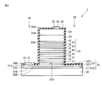
最初に本願発明の実施態様を列記して説明する。本願の半導体積層体は、InP(インジウムリン)からなる基板と、基板上に配置され、1×1021cm-3未満のSbを含むInPからなる第一バッファ層と、第一バッファ層上に配置され、InGaAs(インジウムガリウム砒素)からなる第二バッファ層と、を備える。第一バッファ層は、基板側の主面である第1主面を含むように配置され、基板よりもSbの濃度が高い第一の層を含む。第二バッファ層は、第一バッファ層側の主面である第2主面を含むように配置され、第一の層よりもSbの濃度が低い第二の層を含む。
含んでいる。そのため、受光層の結晶性を優れたものとすることができる。その結果、受光素子の暗電流を低減することができる。したがって、本願の受光素子によれば、高感度な受光素子を得ることができる。
次に、本発明にかかる半導体積層体の実施の形態を、以下に図面を参照しつつ説明する。なお、以下の図面において同一または相当する部分には同一の参照番号を付しその説明は繰返さない。
図1を参照して、実施の形態1における半導体積層体10は、基板20と、バッファ層30と、受光層40と、ブロック層50と、コンタクト層60とを備えている。
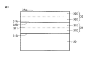
第一の層31Dは、第一バッファ層31全体に形成される他、厚み方向の一部分に形成されるようにしてもよい。図3は、本実施の形態における半導体積層体10の変形例を示す。図3を参照して、第一の層31Dが厚み方向の一部分に形成されている。第一バッファ層31において、第一の層31Dの、基板に面する側とは反対側の主面311上に接触するように、第一の層31DよりもSbの濃度が低い第三の層31Eが配置されている。上述のように第一バッファ層31の表面平坦性を向上させる観点から、基板20に接触する領域にSbの濃度が高い第一の層31Dを配置することが重要である。したがって、第一バッファ層31の全体が第一の層31Dであることは必ずしも必要ではなく、第一の層31Dを基板20に接触する部分に形成する構造を採用した場合でも、表面平坦性に優れた第一バッファ層31を形成することができる。
次に、本発明にかかる半導体装置の他の実施の形態である実施の形態2における受光素子について説明する。図11および図2を参照して、実施の形態2の赤外線受光素子1は、図2に示す構造を単位構造とし、当該単位構造が、基板20の一方の主面20Aに沿う方向に複数繰り返される構造を有している。そして、赤外線受光素子1は、画素に対応する複数のp側電極92を有する。一方、n側電極91は1つだけ配置される。
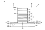
次に、本願の受光素子の実施の形態3について説明する。実施の形態3の赤外線受光素子1は基本的には実施の形態2の赤外線受光素子1と同様の構造を有し、同様の効果を奏する。しかしながら、実施の形態3においては、赤外線受光素子1の画素に対応する単位構造がトレンチ99により分離される構造に代えて、不純物が拡散されていない領域により分離される構造が採用される点において、実施の形態2の場合とは異なっている。以下、実施の形態2の場合とは異なっている点について主に説明する。
10 半導体積層体
20 基板
20A,31A,32A,40A,50A,60A,83A,311 主面
30 バッファ層
31 第一バッファ層
31B 第1主面
31D 第一の層
32D 第二の層
31E 第三の層
32E 第四の層
32 第二バッファ層
32B 第2主面
40 受光層
41,131 第1要素層
42,132 第2要素層
50 ブロック層
60 コンタクト層
61 拡散領域
62 領域
70 読み出し回路
71 本体
72,73,76,77 バンプ
75 配線
80,85 パッシベーション膜
81,82,84,86 開口部
83 マスク層
91,94 n側電極
92,93 p側電極
98,99 トレンチ
98A,99A 側壁
98B,99B 底壁
100 赤外線センサ
Claims (10)
- InPからなる基板と、
前記基板上に配置され、1×1021cm-3未満のSbを含むInPからなる第一バッファ層と、
前記第一バッファ層上に配置され、InGaAsからなる第二バッファ層と、を備え、
前記第一バッファ層は、前記基板側の主面である第1主面を含むように配置され、前記基板よりもSbの濃度が高い第一の層を含み、
前記第二バッファ層は、前記第一バッファ層側の主面である第2主面を含むように配置され、前記第一の層よりもSbの濃度が低い第二の層を含む、半導体積層体。 - 前記第一の層のSbの濃度は、1×1016cm-3以上である、請求項1に記載の半導体積層体。
- 前記第一の層のSbの濃度は、1×1017cm-3以上である、請求項2に記載の半導体積層体。
- 前記第二の層のSbの濃度は、1×1020cm-3以下である、請求項1に記載の半導体積層体。
- 前記第一バッファ層の厚み方向におけるSbの濃度の分布において、Sbの濃度の最大値と最小値との差の前記最大値に対する割合が、50%以下である、請求項1から請求項4のいずれか1項に記載の半導体積層体。
- 前記第一バッファ層の厚みは、10nm以上50nm以下である、請求項1から請求項5のいずれか1項に記載の半導体積層体。
- 前記第二バッファ層上に配置され、III-V族化合物半導体からなる受光層をさらに備える、請求項1から請求項6のいずれか1項に記載の半導体積層体。
- 前記受光層は、タイプII量子井戸構造である、請求項7に記載の半導体積層体。
- 前記タイプII量子井戸構造は、InxGa1-xAs(xは0.38以上1以下)層とGaAs1-ySby(yは0.36以上1以下)層とのペア、またはGa1-uInuNvAs1-v(uは0.4以上0.8以下、vは0を超え0.2以下)層とGaAs1-ySby(yは0.36以上0.62以下)層とのペアを含む多重量子井戸構造である、請求項8に記載の半導体積層体。
- 請求項1から請求項9のいずれか1項に記載の半導体積層体と、
前記半導体積層体上に形成された電極と、を備える、受光素子。
Priority Applications (2)
| Application Number | Priority Date | Filing Date | Title |
|---|---|---|---|
| JP2019004259A JP7147570B2 (ja) | 2019-01-15 | 2019-01-15 | 半導体積層体および受光素子 |
| US16/676,942 US11152521B2 (en) | 2019-01-15 | 2019-11-07 | Semiconductor laminate and light-receiving element |
Applications Claiming Priority (1)
| Application Number | Priority Date | Filing Date | Title |
|---|---|---|---|
| JP2019004259A JP7147570B2 (ja) | 2019-01-15 | 2019-01-15 | 半導体積層体および受光素子 |
Publications (2)
| Publication Number | Publication Date |
|---|---|
| JP2020113668A JP2020113668A (ja) | 2020-07-27 |
| JP7147570B2 true JP7147570B2 (ja) | 2022-10-05 |
Family
ID=71517776
Family Applications (1)
| Application Number | Title | Priority Date | Filing Date |
|---|---|---|---|
| JP2019004259A Active JP7147570B2 (ja) | 2019-01-15 | 2019-01-15 | 半導体積層体および受光素子 |
Country Status (2)
| Country | Link |
|---|---|
| US (1) | US11152521B2 (ja) |
| JP (1) | JP7147570B2 (ja) |
Families Citing this family (1)
| Publication number | Priority date | Publication date | Assignee | Title |
|---|---|---|---|---|
| CN115662876A (zh) * | 2022-08-31 | 2023-01-31 | 珠海庞纳微半导体科技有限公司 | 外延结构及其制备方法 |
Citations (4)
| Publication number | Priority date | Publication date | Assignee | Title |
|---|---|---|---|---|
| US20100258894A1 (en) | 2009-04-08 | 2010-10-14 | Sumitomo Electric Industries, Ltd. | Photodiode array and image pickup device using the same |
| JP2011060853A (ja) | 2009-09-07 | 2011-03-24 | Sumitomo Electric Ind Ltd | Iii−v族化合物半導体受光素子、及びiii−v族化合物半導体受光素子を作製する方法 |
| JP2011100770A (ja) | 2009-11-04 | 2011-05-19 | Sumitomo Electric Ind Ltd | 受光素子アレイの製造方法及び受光素子アレイ、並びにエピタキシャルウェハの製造方法及びエピタキシャルウェハ |
| JP2015082573A (ja) | 2013-10-22 | 2015-04-27 | 住友電気工業株式会社 | エピタキシャルウエハおよびその製造方法 |
Family Cites Families (3)
| Publication number | Priority date | Publication date | Assignee | Title |
|---|---|---|---|---|
| JPH08250752A (ja) * | 1995-03-13 | 1996-09-27 | Advantest Corp | フォトコンダクタ |
| JP2009027046A (ja) * | 2007-07-21 | 2009-02-05 | Sumitomo Electric Ind Ltd | 受光素子 |
| JP4662188B2 (ja) | 2008-02-01 | 2011-03-30 | 住友電気工業株式会社 | 受光素子、受光素子アレイおよびそれらの製造方法 |
-
2019
- 2019-01-15 JP JP2019004259A patent/JP7147570B2/ja active Active
- 2019-11-07 US US16/676,942 patent/US11152521B2/en active Active
Patent Citations (4)
| Publication number | Priority date | Publication date | Assignee | Title |
|---|---|---|---|---|
| US20100258894A1 (en) | 2009-04-08 | 2010-10-14 | Sumitomo Electric Industries, Ltd. | Photodiode array and image pickup device using the same |
| JP2011060853A (ja) | 2009-09-07 | 2011-03-24 | Sumitomo Electric Ind Ltd | Iii−v族化合物半導体受光素子、及びiii−v族化合物半導体受光素子を作製する方法 |
| JP2011100770A (ja) | 2009-11-04 | 2011-05-19 | Sumitomo Electric Ind Ltd | 受光素子アレイの製造方法及び受光素子アレイ、並びにエピタキシャルウェハの製造方法及びエピタキシャルウェハ |
| JP2015082573A (ja) | 2013-10-22 | 2015-04-27 | 住友電気工業株式会社 | エピタキシャルウエハおよびその製造方法 |
Also Published As
| Publication number | Publication date |
|---|---|
| JP2020113668A (ja) | 2020-07-27 |
| US11152521B2 (en) | 2021-10-19 |
| US20200227576A1 (en) | 2020-07-16 |
Similar Documents
| Publication | Publication Date | Title |
|---|---|---|
| JP5975417B2 (ja) | 受光素子の製造方法 | |
| JP2014127499A (ja) | 受光デバイス、その製造法、およびセンシング装置 | |
| JP2016092037A (ja) | 半導体積層体、受光素子およびセンサ | |
| US10326034B2 (en) | Semiconductor laminate and light-receiving element | |
| JP2014236067A (ja) | 半導体素子およびその製造方法 | |
| JP6454981B2 (ja) | 半導体積層体および受光素子 | |
| US10790401B2 (en) | Semiconductor stacked body and light-receiving device | |
| US10158035B2 (en) | Semiconductor stack, light-receiving device, and method for producing semiconductor stack | |
| US9887310B2 (en) | Semiconductor layered structure, method for producing semiconductor layered structure, and method for producing semiconductor device | |
| JP6613923B2 (ja) | 半導体積層体、受光素子および半導体積層体の製造方法 | |
| JP6488855B2 (ja) | 半導体積層体、受光素子および半導体積層体の製造方法 | |
| US11282702B2 (en) | Method of forming a semiconductor device structure | |
| JP7147570B2 (ja) | 半導体積層体および受光素子 | |
| US9929301B2 (en) | Semiconductor stack and semiconductor device | |
| JP6488854B2 (ja) | 半導体積層体および受光素子 | |
| WO2016067996A1 (ja) | 半導体積層体、受光素子およびセンサ | |
| JP6233070B2 (ja) | 半導体積層体および半導体装置、ならびにそれらの製造方法 | |
| US11081605B2 (en) | Semiconductor laminate, light-receiving element, and method for manufacturing semiconductor laminate | |
| WO2012073934A1 (ja) | 受光素子、半導体エピタキシャルウエハ、これらの製造方法および検出装置 |
Legal Events
| Date | Code | Title | Description |
|---|---|---|---|
| A621 | Written request for application examination |
Free format text: JAPANESE INTERMEDIATE CODE: A621 Effective date: 20211021 |
|
| TRDD | Decision of grant or rejection written | ||
| A977 | Report on retrieval |
Free format text: JAPANESE INTERMEDIATE CODE: A971007 Effective date: 20220817 |
|
| A01 | Written decision to grant a patent or to grant a registration (utility model) |
Free format text: JAPANESE INTERMEDIATE CODE: A01 Effective date: 20220823 |
|
| A61 | First payment of annual fees (during grant procedure) |
Free format text: JAPANESE INTERMEDIATE CODE: A61 Effective date: 20220905 |
|
| R150 | Certificate of patent or registration of utility model |
Ref document number: 7147570 Country of ref document: JP Free format text: JAPANESE INTERMEDIATE CODE: R150 |
|
| R250 | Receipt of annual fees |
Free format text: JAPANESE INTERMEDIATE CODE: R250 |