JP7182906B2 - 表示装置及び電子機器 - Google Patents
表示装置及び電子機器 Download PDFInfo
- Publication number
- JP7182906B2 JP7182906B2 JP2018111851A JP2018111851A JP7182906B2 JP 7182906 B2 JP7182906 B2 JP 7182906B2 JP 2018111851 A JP2018111851 A JP 2018111851A JP 2018111851 A JP2018111851 A JP 2018111851A JP 7182906 B2 JP7182906 B2 JP 7182906B2
- Authority
- JP
- Japan
- Prior art keywords
- liquid crystal
- camera
- crystal panel
- guide plate
- pixel
- Prior art date
- Legal status (The legal status is an assumption and is not a legal conclusion. Google has not performed a legal analysis and makes no representation as to the accuracy of the status listed.)
- Active
Links
Images



Classifications
-
- G—PHYSICS
- G02—OPTICS
- G02F—OPTICAL DEVICES OR ARRANGEMENTS FOR THE CONTROL OF LIGHT BY MODIFICATION OF THE OPTICAL PROPERTIES OF THE MEDIA OF THE ELEMENTS INVOLVED THEREIN; NON-LINEAR OPTICS; FREQUENCY-CHANGING OF LIGHT; OPTICAL LOGIC ELEMENTS; OPTICAL ANALOGUE/DIGITAL CONVERTERS
- G02F1/00—Devices or arrangements for the control of the intensity, colour, phase, polarisation or direction of light arriving from an independent light source, e.g. switching, gating or modulating; Non-linear optics
- G02F1/01—Devices or arrangements for the control of the intensity, colour, phase, polarisation or direction of light arriving from an independent light source, e.g. switching, gating or modulating; Non-linear optics for the control of the intensity, phase, polarisation or colour
- G02F1/13—Devices or arrangements for the control of the intensity, colour, phase, polarisation or direction of light arriving from an independent light source, e.g. switching, gating or modulating; Non-linear optics for the control of the intensity, phase, polarisation or colour based on liquid crystals, e.g. single liquid crystal display cells
- G02F1/133—Constructional arrangements; Operation of liquid crystal cells; Circuit arrangements
- G02F1/13306—Circuit arrangements or driving methods for the control of single liquid crystal cells
- G02F1/13312—Circuits comprising photodetectors for purposes other than feedback
-
- G—PHYSICS
- G02—OPTICS
- G02F—OPTICAL DEVICES OR ARRANGEMENTS FOR THE CONTROL OF LIGHT BY MODIFICATION OF THE OPTICAL PROPERTIES OF THE MEDIA OF THE ELEMENTS INVOLVED THEREIN; NON-LINEAR OPTICS; FREQUENCY-CHANGING OF LIGHT; OPTICAL LOGIC ELEMENTS; OPTICAL ANALOGUE/DIGITAL CONVERTERS
- G02F1/00—Devices or arrangements for the control of the intensity, colour, phase, polarisation or direction of light arriving from an independent light source, e.g. switching, gating or modulating; Non-linear optics
- G02F1/01—Devices or arrangements for the control of the intensity, colour, phase, polarisation or direction of light arriving from an independent light source, e.g. switching, gating or modulating; Non-linear optics for the control of the intensity, phase, polarisation or colour
- G02F1/13—Devices or arrangements for the control of the intensity, colour, phase, polarisation or direction of light arriving from an independent light source, e.g. switching, gating or modulating; Non-linear optics for the control of the intensity, phase, polarisation or colour based on liquid crystals, e.g. single liquid crystal display cells
- G02F1/133—Constructional arrangements; Operation of liquid crystal cells; Circuit arrangements
- G02F1/1333—Constructional arrangements; Manufacturing methods
- G02F1/1335—Structural association of cells with optical devices, e.g. polarisers or reflectors
- G02F1/133553—Reflecting elements
-
- F—MECHANICAL ENGINEERING; LIGHTING; HEATING; WEAPONS; BLASTING
- F21—LIGHTING
- F21S—NON-PORTABLE LIGHTING DEVICES; SYSTEMS THEREOF; VEHICLE LIGHTING DEVICES SPECIALLY ADAPTED FOR VEHICLE EXTERIORS
- F21S2/00—Systems of lighting devices, not provided for in main groups F21S4/00 - F21S10/00 or F21S19/00, e.g. of modular construction
-
- G—PHYSICS
- G02—OPTICS
- G02F—OPTICAL DEVICES OR ARRANGEMENTS FOR THE CONTROL OF LIGHT BY MODIFICATION OF THE OPTICAL PROPERTIES OF THE MEDIA OF THE ELEMENTS INVOLVED THEREIN; NON-LINEAR OPTICS; FREQUENCY-CHANGING OF LIGHT; OPTICAL LOGIC ELEMENTS; OPTICAL ANALOGUE/DIGITAL CONVERTERS
- G02F1/00—Devices or arrangements for the control of the intensity, colour, phase, polarisation or direction of light arriving from an independent light source, e.g. switching, gating or modulating; Non-linear optics
- G02F1/01—Devices or arrangements for the control of the intensity, colour, phase, polarisation or direction of light arriving from an independent light source, e.g. switching, gating or modulating; Non-linear optics for the control of the intensity, phase, polarisation or colour
- G02F1/13—Devices or arrangements for the control of the intensity, colour, phase, polarisation or direction of light arriving from an independent light source, e.g. switching, gating or modulating; Non-linear optics for the control of the intensity, phase, polarisation or colour based on liquid crystals, e.g. single liquid crystal display cells
- G02F1/133—Constructional arrangements; Operation of liquid crystal cells; Circuit arrangements
- G02F1/1333—Constructional arrangements; Manufacturing methods
- G02F1/13338—Input devices, e.g. touch panels
-
- G—PHYSICS
- G02—OPTICS
- G02F—OPTICAL DEVICES OR ARRANGEMENTS FOR THE CONTROL OF LIGHT BY MODIFICATION OF THE OPTICAL PROPERTIES OF THE MEDIA OF THE ELEMENTS INVOLVED THEREIN; NON-LINEAR OPTICS; FREQUENCY-CHANGING OF LIGHT; OPTICAL LOGIC ELEMENTS; OPTICAL ANALOGUE/DIGITAL CONVERTERS
- G02F1/00—Devices or arrangements for the control of the intensity, colour, phase, polarisation or direction of light arriving from an independent light source, e.g. switching, gating or modulating; Non-linear optics
- G02F1/01—Devices or arrangements for the control of the intensity, colour, phase, polarisation or direction of light arriving from an independent light source, e.g. switching, gating or modulating; Non-linear optics for the control of the intensity, phase, polarisation or colour
- G02F1/13—Devices or arrangements for the control of the intensity, colour, phase, polarisation or direction of light arriving from an independent light source, e.g. switching, gating or modulating; Non-linear optics for the control of the intensity, phase, polarisation or colour based on liquid crystals, e.g. single liquid crystal display cells
- G02F1/133—Constructional arrangements; Operation of liquid crystal cells; Circuit arrangements
- G02F1/1333—Constructional arrangements; Manufacturing methods
- G02F1/1335—Structural association of cells with optical devices, e.g. polarisers or reflectors
- G02F1/133509—Filters, e.g. light shielding masks
- G02F1/133514—Colour filters
-
- G—PHYSICS
- G02—OPTICS
- G02F—OPTICAL DEVICES OR ARRANGEMENTS FOR THE CONTROL OF LIGHT BY MODIFICATION OF THE OPTICAL PROPERTIES OF THE MEDIA OF THE ELEMENTS INVOLVED THEREIN; NON-LINEAR OPTICS; FREQUENCY-CHANGING OF LIGHT; OPTICAL LOGIC ELEMENTS; OPTICAL ANALOGUE/DIGITAL CONVERTERS
- G02F1/00—Devices or arrangements for the control of the intensity, colour, phase, polarisation or direction of light arriving from an independent light source, e.g. switching, gating or modulating; Non-linear optics
- G02F1/01—Devices or arrangements for the control of the intensity, colour, phase, polarisation or direction of light arriving from an independent light source, e.g. switching, gating or modulating; Non-linear optics for the control of the intensity, phase, polarisation or colour
- G02F1/13—Devices or arrangements for the control of the intensity, colour, phase, polarisation or direction of light arriving from an independent light source, e.g. switching, gating or modulating; Non-linear optics for the control of the intensity, phase, polarisation or colour based on liquid crystals, e.g. single liquid crystal display cells
- G02F1/133—Constructional arrangements; Operation of liquid crystal cells; Circuit arrangements
- G02F1/1333—Constructional arrangements; Manufacturing methods
- G02F1/1335—Structural association of cells with optical devices, e.g. polarisers or reflectors
- G02F1/133524—Light-guides, e.g. fibre-optic bundles, louvered or jalousie light-guides
-
- G—PHYSICS
- G02—OPTICS
- G02F—OPTICAL DEVICES OR ARRANGEMENTS FOR THE CONTROL OF LIGHT BY MODIFICATION OF THE OPTICAL PROPERTIES OF THE MEDIA OF THE ELEMENTS INVOLVED THEREIN; NON-LINEAR OPTICS; FREQUENCY-CHANGING OF LIGHT; OPTICAL LOGIC ELEMENTS; OPTICAL ANALOGUE/DIGITAL CONVERTERS
- G02F1/00—Devices or arrangements for the control of the intensity, colour, phase, polarisation or direction of light arriving from an independent light source, e.g. switching, gating or modulating; Non-linear optics
- G02F1/01—Devices or arrangements for the control of the intensity, colour, phase, polarisation or direction of light arriving from an independent light source, e.g. switching, gating or modulating; Non-linear optics for the control of the intensity, phase, polarisation or colour
- G02F1/13—Devices or arrangements for the control of the intensity, colour, phase, polarisation or direction of light arriving from an independent light source, e.g. switching, gating or modulating; Non-linear optics for the control of the intensity, phase, polarisation or colour based on liquid crystals, e.g. single liquid crystal display cells
- G02F1/133—Constructional arrangements; Operation of liquid crystal cells; Circuit arrangements
- G02F1/1333—Constructional arrangements; Manufacturing methods
- G02F1/1335—Structural association of cells with optical devices, e.g. polarisers or reflectors
- G02F1/133528—Polarisers
-
- G—PHYSICS
- G03—PHOTOGRAPHY; CINEMATOGRAPHY; ANALOGOUS TECHNIQUES USING WAVES OTHER THAN OPTICAL WAVES; ELECTROGRAPHY; HOLOGRAPHY
- G03B—APPARATUS OR ARRANGEMENTS FOR TAKING PHOTOGRAPHS OR FOR PROJECTING OR VIEWING THEM; APPARATUS OR ARRANGEMENTS EMPLOYING ANALOGOUS TECHNIQUES USING WAVES OTHER THAN OPTICAL WAVES; ACCESSORIES THEREFOR
- G03B17/00—Details of cameras or camera bodies; Accessories therefor
- G03B17/18—Signals indicating condition of a camera member or suitability of light
-
- H—ELECTRICITY
- H04—ELECTRIC COMMUNICATION TECHNIQUE
- H04M—TELEPHONIC COMMUNICATION
- H04M1/00—Substation equipment, e.g. for use by subscribers
- H04M1/02—Constructional features of telephone sets
- H04M1/0202—Portable telephone sets, e.g. cordless phones, mobile phones or bar type handsets
- H04M1/026—Details of the structure or mounting of specific components
- H04M1/0264—Details of the structure or mounting of specific components for a camera module assembly
-
- H—ELECTRICITY
- H04—ELECTRIC COMMUNICATION TECHNIQUE
- H04M—TELEPHONIC COMMUNICATION
- H04M1/00—Substation equipment, e.g. for use by subscribers
- H04M1/02—Constructional features of telephone sets
- H04M1/0202—Portable telephone sets, e.g. cordless phones, mobile phones or bar type handsets
- H04M1/026—Details of the structure or mounting of specific components
- H04M1/0266—Details of the structure or mounting of specific components for a display module assembly
-
- H—ELECTRICITY
- H04—ELECTRIC COMMUNICATION TECHNIQUE
- H04N—PICTORIAL COMMUNICATION, e.g. TELEVISION
- H04N23/00—Cameras or camera modules comprising electronic image sensors; Control thereof
Landscapes
- Physics & Mathematics (AREA)
- Nonlinear Science (AREA)
- General Physics & Mathematics (AREA)
- Optics & Photonics (AREA)
- Mathematical Physics (AREA)
- Chemical & Material Sciences (AREA)
- Crystallography & Structural Chemistry (AREA)
- Engineering & Computer Science (AREA)
- Signal Processing (AREA)
- Multimedia (AREA)
- Liquid Crystal (AREA)
- General Engineering & Computer Science (AREA)
- Devices For Indicating Variable Information By Combining Individual Elements (AREA)
- Planar Illumination Modules (AREA)
- Studio Devices (AREA)
- Indication In Cameras, And Counting Of Exposures (AREA)
Description
カメラと、
前記カメラに重畳する表示部を備えた液晶パネルと、
第1側面と、前記液晶パネルに対向する主面と、第1貫通孔と、を有する導光板と、
前記第1側面に対向する光源と、を備え、
前記カメラは、前記第1貫通孔に設けられている、電子機器が提供される。
本実施形態によれば、
カメラと、
前記カメラに重畳する表示部を備えた液晶パネルと、
第1側面と、前記第1側面の反対側の第2側面と、前記液晶パネルに対向する第1主面と、を有する第1導光板と、
前記第1側面に対向する第1光源と、
前記第2側面に対向する第3側面と、第4側面と、前記液晶パネルに対向する第2主面と、第1貫通孔と、を有する第2導光板と、
前記第4側面に対向する第2光源と、を備え、
前記第1側面、前記第2側面、及び、前記第3側面は、第1方向に沿って延出し、
前記第4側面は、前記第1方向と交差する第2方向に沿って延出し、
前記カメラは、前記第1貫通孔に設けられている、電子機器が提供される。
本実施形態によれば、
面状光源と、
前記面状光源上に配置される液晶素子と、
前記液晶素子を駆動する駆動部と、を備えた表示装置であって、
前記面状光源の一部には貫通孔が設けられ、
前記駆動部は、前記面状光源の前記貫通孔内または前記貫通孔を通して配置されるカメラに撮像光を導くように、前記貫通孔に対応する領域の前記液晶素子の透過率を制御する、表示装置が提供される。
このような表示装置DSPを組み込んだ電子機器100は、カメラ1を備えている。
第1絶縁基板10及び第2絶縁基板20は、ガラス基板や可撓性の樹脂基板などの透明基板である。配向膜AL1及びAL2は、液晶層LCに接している。
カラーフィルタ層CF、遮光層BMA、及び、透明層OCは、第2絶縁基板20と液晶層LCとの間に位置している。
遮光層BMAは、非表示部NDAに位置している。表示部DAと非表示部NDAとの境界Bは、遮光層BMAの内側端に相当する。シールSEは、遮光層BMAと重畳する位置に設けられている。
カラーフィルタ層CFの詳細については、ここでは省略するが、例えば、カラーフィルタ層CFは、赤色、緑色、青色のそれぞれのカラーフィルタを備えている。透明層OCは、カラーフィルタ層CF及び遮光層BMを覆っている。透明層OCは、例えば、透明な有機絶縁膜である。
第1画素PX1において、液晶層LCに電圧が印加されていないオフ状態では、液晶層LCに含まれる液晶分子LMは、配向膜AL1及びAL2の間で所定の方向に初期配向している。このようなオフ状態では、図1に示した光源EMから第1画素PX1に導光された光は、第1偏光板PL1及び第2偏光板PL2によって吸収される。このため、オフ状態の第1画素PX1は、黒を表示する。
一方、液晶層LCに電圧が印加されたオン状態では、液晶分子LMは、画素電極PEと共通電極CEとの間に形成された電界により初期配向方向とは異なる方向に配向し、その配向方向は電界によって制御される。このようなオン状態では、第1画素PX1に導光された光の一部は、第1偏光板PL1及び第2偏光板PL2を透過する。このため、オン状態の第1画素PX1は、カラーフィルタ層CFに応じた色を表示する。
一方、液晶層LCに電圧が印加されたオン状態では、第2画素PX2に導光された光の一部は、第1偏光板PL1及び第2偏光板PL2を透過する。オン状態の第2画素PX2は、最大透過率の場合に、白を表示する、あるいは、透明状態となる。また、上記の通り、第2画素PX2は、最小透過率と最大透過率との間の透過率となるように制御され、グレーを表示する場合もありうる。
尚、本実施形態では、第1領域A1と第2領域A2とに遮光層BMBが形成されているが、第2領域A2における遮光層BMBの幅を、第1領域A1における遮光層BMBの幅よりも狭くしてもよい。更には、第2領域A2に遮光層BMBを設けなくてもよい。遮光層BMBの幅を狭くする、或いは、遮光層BMBを設けないのは、第1方向X又は第2方向Yの一方だけでもよく、第1方向X及び第2方向Yの双方向であってもよい。
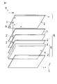
光学シートOSは、第1導光板LG1と液晶パネルPNLとの間、及び、第2導光板LG2と液晶パネルPNLとの間に延在している。光学シートOSは、第1貫通孔TH1に重畳する第2貫通孔TH2を有している。
第1導光板LG1及び第2導光板LG2は、反射シートRSと光学シートOSとの間に位置している。反射シートRSは、第1貫通孔TH1に重畳する第3貫通孔TH3を有している。
カメラ1は、図2を参照して説明したのと同様に、第1貫通孔TH1に設けられている。
第1領域A1に含まれる画素は、図4を参照して説明した第1画素PX1に相当し、カメラ1による撮影画像を表示する。
図8の(B)は、カメラ1を未使用時の表示例に相当する。第2領域A2には、数字、文字、記号、マークなどのキャラクタがモノクロ表示される。また、カメラ1に重畳する位置においても、キャラクタの表示が可能である。第1領域A1には、図示したようなホーム画面の他に、静止画、動画などがカラー表示される。
また、上記した実施形態では、光源EMとして白色の発光ダイオード(LED)を使用した例を示したが、赤、青、緑等の異なる発光色の発光ダイオード(LED)を並置して用いても良い。またこの場合は、各色の発光ダイオード(LED)を順次発光させ、これに合わせて各色表示を順次切り替えることで、カラー表示を実現する、所謂フィールドシーケンシャル方式を用いることもできる。これにより、表示部DAの第1領域A1及び第2領域A2共にカラーフィルタ層CFを配置することなく、いずれの領域もカラー表示を実現することができる。また、第1領域A1にはカラーフィルタ層CFが配置される一方で、第2領域A2にはカラーフィルタ層CFが配置されず、第2領域A2においてフィールドシーケンシャル方式を用いてカラー表示を実現してもよい。
Claims (7)
- カメラと、
前記カメラに重畳する表示部を備えた液晶パネルと、
第1側面と、前記第1側面の反対側の第2側面と、前記液晶パネルに対向する第1主面と、を有する第1導光板と、
前記第1側面に対向する第1光源と、
前記第2側面に対向する第3側面と、第4側面と、前記液晶パネルに対向する第2主面と、第1貫通孔と、を有する第2導光板と、
前記第4側面に対向する第2光源と、を備え、
前記第1側面、前記第2側面、及び、前記第3側面は、第1方向に沿って延出し、
前記第4側面は、前記第1方向と交差する第2方向に沿って延出し、
前記カメラは、前記第1貫通孔に設けられている、電子機器。 - さらに、前記第2側面と前記第3側面との間に位置する遮光層を備えた、請求項1に記載の電子機器。
- さらに、前記第1導光板と前記液晶パネルとの間、及び、前記第2導光板と前記液晶パネルとの間に延在する光学シートを備え、
前記光学シートは、前記第1貫通孔に重畳する第2貫通孔を有している、請求項1または2に記載の電子機器。 - さらに、反射シートを備え、
前記第1導光板及び前記第2導光板は、前記反射シートと前記光学シートとの間に位置し、
前記反射シートは、前記第1貫通孔に重畳する第3貫通孔を有している、請求項3に記載の電子機器。 - さらに、第1偏光板と、第2偏光板と、を備え、
前記液晶パネルは、前記第1偏光板と前記第2偏光板との間に位置し、
前記第1偏光板及び前記第2偏光板は、前記カメラに重畳している、請求項1乃至4のいずれか1項に記載の電子機器。 - 前記液晶パネルは、前記表示部において、
前記カメラに重畳しない第1画素と、
前記カメラに重畳する第2画素と、
前記第1画素に配置されたカラーフィルタ層と、を備え、
前記カラーフィルタ層は、前記第2画素に配置されていない、請求項1乃至5のいずれか1項に記載の電子機器。 - 前記液晶パネルは、さらに、
第1絶縁基板と、
第2絶縁基板と、
前記第1絶縁基板と前記第2絶縁基板との間に位置する液晶層と、
前記カラーフィルタ層を覆う透明層と、を備え、
前記カラーフィルタ層及び前記透明層は、前記第2絶縁基板と前記液晶層との間に位置し、
前記第2画素において、前記透明層は、前記第2絶縁基板に接している、請求項6に記載の電子機器。
Priority Applications (6)
| Application Number | Priority Date | Filing Date | Title |
|---|---|---|---|
| JP2018111851A JP7182906B2 (ja) | 2018-06-12 | 2018-06-12 | 表示装置及び電子機器 |
| DE112019002422.1T DE112019002422B4 (de) | 2018-06-12 | 2019-05-24 | Elektronisches Gerät |
| CN201980038964.6A CN112262340A (zh) | 2018-06-12 | 2019-05-24 | 显示装置及电子设备 |
| PCT/JP2019/020782 WO2019239861A1 (ja) | 2018-06-12 | 2019-05-24 | 表示装置及び電子機器 |
| US17/110,374 US11668972B2 (en) | 2018-06-12 | 2020-12-03 | Display device and electronic apparatus |
| US18/168,087 US11982900B2 (en) | 2018-06-12 | 2023-02-13 | Display device and electronic apparatus |
Applications Claiming Priority (1)
| Application Number | Priority Date | Filing Date | Title |
|---|---|---|---|
| JP2018111851A JP7182906B2 (ja) | 2018-06-12 | 2018-06-12 | 表示装置及び電子機器 |
Publications (2)
| Publication Number | Publication Date |
|---|---|
| JP2019215415A JP2019215415A (ja) | 2019-12-19 |
| JP7182906B2 true JP7182906B2 (ja) | 2022-12-05 |
Family
ID=68842988
Family Applications (1)
| Application Number | Title | Priority Date | Filing Date |
|---|---|---|---|
| JP2018111851A Active JP7182906B2 (ja) | 2018-06-12 | 2018-06-12 | 表示装置及び電子機器 |
Country Status (5)
| Country | Link |
|---|---|
| US (2) | US11668972B2 (ja) |
| JP (1) | JP7182906B2 (ja) |
| CN (1) | CN112262340A (ja) |
| DE (1) | DE112019002422B4 (ja) |
| WO (1) | WO2019239861A1 (ja) |
Families Citing this family (11)
| Publication number | Priority date | Publication date | Assignee | Title |
|---|---|---|---|---|
| CN111524932A (zh) * | 2019-02-01 | 2020-08-11 | Oppo广东移动通信有限公司 | 电子设备、像素结构及显示装置 |
| CN110441958A (zh) * | 2019-07-05 | 2019-11-12 | 武汉华星光电技术有限公司 | 一种显示面板模组 |
| CN111176018A (zh) * | 2020-02-12 | 2020-05-19 | 武汉华星光电技术有限公司 | 一种显示装置 |
| CN111198458A (zh) * | 2020-03-02 | 2020-05-26 | 武汉华星光电技术有限公司 | 显示装置 |
| CN111458935A (zh) * | 2020-04-23 | 2020-07-28 | 捷开通讯(深圳)有限公司 | 一种显示面板及终端 |
| KR20210137856A (ko) | 2020-05-11 | 2021-11-18 | 삼성전자주식회사 | 디스플레이 및 카메라를 포함하는 전자 장치 |
| CN111610665A (zh) * | 2020-06-30 | 2020-09-01 | 上海摩软通讯技术有限公司 | 显示组件与移动终端 |
| WO2022050566A1 (ko) * | 2020-09-03 | 2022-03-10 | 삼성전자 주식회사 | 슬라이더블 전자 장치 및 상기 전자 장치에서 투명 디스플레이를 이용하는 방법 |
| JP2022110490A (ja) * | 2021-01-18 | 2022-07-29 | ミネベアミツミ株式会社 | 面状照明装置 |
| WO2023221126A1 (zh) * | 2022-05-20 | 2023-11-23 | 京东方科技集团股份有限公司 | 显示基板及其制备方法、显示装置 |
| TWI903828B (zh) | 2024-10-25 | 2025-11-01 | 友達光電股份有限公司 | 顯示裝置 |
Citations (4)
| Publication number | Priority date | Publication date | Assignee | Title |
|---|---|---|---|---|
| JP2000075282A (ja) | 1998-09-02 | 2000-03-14 | Casio Comput Co Ltd | 液晶表示装置 |
| US20140096053A1 (en) | 2012-10-02 | 2014-04-03 | Lg Electronics Inc. | Mobile terminal and control method for the mobile terminal |
| WO2015022887A1 (ja) | 2013-08-12 | 2015-02-19 | シャープ株式会社 | 表示装置 |
| WO2018083817A1 (ja) | 2016-11-07 | 2018-05-11 | 京セラディスプレイ株式会社 | 画像表示装置 |
Family Cites Families (20)
| Publication number | Priority date | Publication date | Assignee | Title |
|---|---|---|---|---|
| TWI237144B (en) * | 2002-11-19 | 2005-08-01 | Benq Corp | Display apparatus and light guide unit thereof |
| JP2006350338A (ja) * | 2005-06-13 | 2006-12-28 | Samsung Electronics Co Ltd | バックライトアセンブリとこれを有する表示装置及びその輝度調節方法 |
| KR20070119227A (ko) * | 2006-06-14 | 2007-12-20 | 삼성전자주식회사 | 액정 표시 모듈 |
| US8154582B2 (en) | 2007-10-19 | 2012-04-10 | Eastman Kodak Company | Display device with capture capabilities |
| US7740390B2 (en) * | 2007-11-16 | 2010-06-22 | Avago Technologies Ecbu Ip (Singapore) Pte, Ltd. | Segmented light guide |
| US8104945B2 (en) * | 2007-12-27 | 2012-01-31 | Samsung Led Co., Ltd. | Backlight unit implementing local dimming for liquid crystal display device |
| JPWO2009098809A1 (ja) * | 2008-02-05 | 2011-05-26 | シャープ株式会社 | 照明装置および液晶表示装置 |
| US20110205453A1 (en) * | 2008-10-23 | 2011-08-25 | Sharp Kabushiki Kaisha | Illumination device, surface illuminant device, display device, and television receiver |
| JP2013061436A (ja) | 2011-09-13 | 2013-04-04 | Lenovo Singapore Pte Ltd | 液晶シャッタを備える電子機器 |
| US8867015B2 (en) * | 2012-01-11 | 2014-10-21 | Apple Inc. | Displays with liquid crystal shutters |
| WO2014103917A1 (ja) * | 2012-12-28 | 2014-07-03 | シャープ株式会社 | 液晶ディスプレイ |
| US9806219B2 (en) * | 2013-02-14 | 2017-10-31 | Apple Inc. | Displays with camera window openings |
| JP6365184B2 (ja) * | 2014-09-26 | 2018-08-01 | 日亜化学工業株式会社 | 液晶表示装置用バックライトユニット及びこれを用いた液晶表示装置 |
| KR102289904B1 (ko) * | 2015-01-23 | 2021-08-18 | 삼성디스플레이 주식회사 | 표시 장치 |
| KR101596848B1 (ko) * | 2015-03-02 | 2016-02-23 | 엘지전자 주식회사 | 디스플레이 패널 및 이동 단말기 |
| KR102485165B1 (ko) | 2015-08-21 | 2023-01-09 | 삼성디스플레이 주식회사 | 표시 장치 및 그 구동 방법 |
| KR20170052808A (ko) * | 2015-11-04 | 2017-05-15 | 삼성디스플레이 주식회사 | 백라이트 유닛 및 이를 포함한 표시장치 |
| KR102501111B1 (ko) * | 2015-12-28 | 2023-02-16 | 엘지디스플레이 주식회사 | 카메라 모듈 일체형 액정 표시 장치 및 그 제조 방법 |
| US10191577B2 (en) * | 2016-02-16 | 2019-01-29 | Samsung Electronics Co., Ltd. | Electronic device |
| CN107784989B (zh) * | 2017-10-27 | 2020-04-14 | 信利光电股份有限公司 | 一种带摄像模组的液晶显示装置 |
-
2018
- 2018-06-12 JP JP2018111851A patent/JP7182906B2/ja active Active
-
2019
- 2019-05-24 DE DE112019002422.1T patent/DE112019002422B4/de active Active
- 2019-05-24 WO PCT/JP2019/020782 patent/WO2019239861A1/ja not_active Ceased
- 2019-05-24 CN CN201980038964.6A patent/CN112262340A/zh active Pending
-
2020
- 2020-12-03 US US17/110,374 patent/US11668972B2/en active Active
-
2023
- 2023-02-13 US US18/168,087 patent/US11982900B2/en active Active
Patent Citations (4)
| Publication number | Priority date | Publication date | Assignee | Title |
|---|---|---|---|---|
| JP2000075282A (ja) | 1998-09-02 | 2000-03-14 | Casio Comput Co Ltd | 液晶表示装置 |
| US20140096053A1 (en) | 2012-10-02 | 2014-04-03 | Lg Electronics Inc. | Mobile terminal and control method for the mobile terminal |
| WO2015022887A1 (ja) | 2013-08-12 | 2015-02-19 | シャープ株式会社 | 表示装置 |
| WO2018083817A1 (ja) | 2016-11-07 | 2018-05-11 | 京セラディスプレイ株式会社 | 画像表示装置 |
Also Published As
| Publication number | Publication date |
|---|---|
| DE112019002422B4 (de) | 2023-06-29 |
| US20210088842A1 (en) | 2021-03-25 |
| US20230194920A1 (en) | 2023-06-22 |
| US11982900B2 (en) | 2024-05-14 |
| US11668972B2 (en) | 2023-06-06 |
| DE112019002422T5 (de) | 2021-04-08 |
| WO2019239861A1 (ja) | 2019-12-19 |
| JP2019215415A (ja) | 2019-12-19 |
| CN112262340A (zh) | 2021-01-22 |
Similar Documents
| Publication | Publication Date | Title |
|---|---|---|
| JP7182906B2 (ja) | 表示装置及び電子機器 | |
| CN112313567B (zh) | 显示装置、嵌入有显示装置的电子设备以及存储介质 | |
| US11422298B2 (en) | Electronic device | |
| JP7123758B2 (ja) | 電子機器 | |
| CN107615154B (zh) | 液晶显示装置及平视显示器装置 | |
| US11703722B2 (en) | Electronic device | |
| JP7229789B2 (ja) | 表示装置、及び、表示装置を組み込んだ電子機器 | |
| US11579499B2 (en) | Electronic apparatus | |
| WO2020202925A1 (ja) | 電子機器 | |
| WO2020202924A1 (ja) | 電子機器 | |
| JP2022087540A (ja) | 表示装置又は電子機器 | |
| JP2021162817A (ja) | 電子機器 | |
| WO2020137221A1 (ja) | 表示装置、及び、表示装置を組み込んだ電子機器 | |
| WO2021220846A1 (ja) | 表示装置 |
Legal Events
| Date | Code | Title | Description |
|---|---|---|---|
| A621 | Written request for application examination |
Free format text: JAPANESE INTERMEDIATE CODE: A621 Effective date: 20210517 |
|
| A131 | Notification of reasons for refusal |
Free format text: JAPANESE INTERMEDIATE CODE: A131 Effective date: 20220621 |
|
| A521 | Request for written amendment filed |
Free format text: JAPANESE INTERMEDIATE CODE: A523 Effective date: 20220812 |
|
| TRDD | Decision of grant or rejection written | ||
| A01 | Written decision to grant a patent or to grant a registration (utility model) |
Free format text: JAPANESE INTERMEDIATE CODE: A01 Effective date: 20221101 |
|
| A61 | First payment of annual fees (during grant procedure) |
Free format text: JAPANESE INTERMEDIATE CODE: A61 Effective date: 20221122 |
|
| R150 | Certificate of patent or registration of utility model |
Ref document number: 7182906 Country of ref document: JP Free format text: JAPANESE INTERMEDIATE CODE: R150 |
|
| S111 | Request for change of ownership or part of ownership |
Free format text: JAPANESE INTERMEDIATE CODE: R313113 |
|
| R350 | Written notification of registration of transfer |
Free format text: JAPANESE INTERMEDIATE CODE: R350 |
|
| R250 | Receipt of annual fees |
Free format text: JAPANESE INTERMEDIATE CODE: R250 |