JP7200460B2 - package structure - Google Patents
package structure Download PDFInfo
- Publication number
- JP7200460B2 JP7200460B2 JP2019100507A JP2019100507A JP7200460B2 JP 7200460 B2 JP7200460 B2 JP 7200460B2 JP 2019100507 A JP2019100507 A JP 2019100507A JP 2019100507 A JP2019100507 A JP 2019100507A JP 7200460 B2 JP7200460 B2 JP 7200460B2
- Authority
- JP
- Japan
- Prior art keywords
- substrate
- package structure
- stiffener
- reinforcing member
- interposer
- Prior art date
- Legal status (The legal status is an assumption and is not a legal conclusion. Google has not performed a legal analysis and makes no representation as to the accuracy of the status listed.)
- Active
Links
Images

Classifications
-
- H—ELECTRICITY
- H10—SEMICONDUCTOR DEVICES; ELECTRIC SOLID-STATE DEVICES NOT OTHERWISE PROVIDED FOR
- H10W—GENERIC PACKAGES, INTERCONNECTIONS, CONNECTORS OR OTHER CONSTRUCTIONAL DETAILS OF DEVICES COVERED BY CLASS H10
- H10W72/00—Interconnections or connectors in packages
- H10W72/01—Manufacture or treatment
- H10W72/0198—Manufacture or treatment batch processes
-
- H—ELECTRICITY
- H10—SEMICONDUCTOR DEVICES; ELECTRIC SOLID-STATE DEVICES NOT OTHERWISE PROVIDED FOR
- H10W—GENERIC PACKAGES, INTERCONNECTIONS, CONNECTORS OR OTHER CONSTRUCTIONAL DETAILS OF DEVICES COVERED BY CLASS H10
- H10W70/00—Package substrates; Interposers; Redistribution layers [RDL]
- H10W70/60—Insulating or insulated package substrates; Interposers; Redistribution layers
- H10W70/67—Insulating or insulated package substrates; Interposers; Redistribution layers characterised by their insulating layers or insulating parts
- H10W70/68—Shapes or dispositions thereof
-
- H—ELECTRICITY
- H10—SEMICONDUCTOR DEVICES; ELECTRIC SOLID-STATE DEVICES NOT OTHERWISE PROVIDED FOR
- H10W—GENERIC PACKAGES, INTERCONNECTIONS, CONNECTORS OR OTHER CONSTRUCTIONAL DETAILS OF DEVICES COVERED BY CLASS H10
- H10W74/00—Encapsulations, e.g. protective coatings
- H10W74/40—Encapsulations, e.g. protective coatings characterised by their materials
-
- H—ELECTRICITY
- H10—SEMICONDUCTOR DEVICES; ELECTRIC SOLID-STATE DEVICES NOT OTHERWISE PROVIDED FOR
- H10W—GENERIC PACKAGES, INTERCONNECTIONS, CONNECTORS OR OTHER CONSTRUCTIONAL DETAILS OF DEVICES COVERED BY CLASS H10
- H10W78/00—Detachable holders for supporting packaged chips in operation
Landscapes
- Structure Of Printed Boards (AREA)
- Combinations Of Printed Boards (AREA)
Description
本発明は、パッケージ構造物(Package Structure)に関する。 The present invention relates to package structures.
各種電子機器の使用が爆発的に増加するとともにデジタル技術及び半導体技術等の発達により、精密かつ複雑な電子機器の応用分野が広範囲になっている。電子機器の内部部品の密集度が高くなることにより、個々の部品(active、passive)を接続させるために必要なPCBの面積が大きくなっている。一方、バッテリーの大きさは大きくなる傾向にあり、このため、電子機器の限定された空間内にPCBを効率的に配置、装着する必要がある。 With the explosive increase in the use of various electronic devices and the development of digital technology and semiconductor technology, the fields of application of precision and complex electronic devices are expanding. Due to the high density of internal components in electronic equipment, the PCB area required to connect individual components (active and passive) is increasing. On the other hand, the size of batteries tends to increase, so there is a need to efficiently arrange and mount PCBs in the limited space of electronic devices.
本発明の一側面によれば、インターポーザで上下に結合された第1基板及び第2基板と、上記第1基板の上記第2基板と向かい合う一面に実装された第1素子と、上記第1基板の上記一面に上記第1素子から離隔して付着される補強材と、上記補強材の向かい側に位置するように、上記第2基板の一面に実装される第2素子と、を含むパッケージ構造物が提供される。 According to one aspect of the present invention, a first substrate and a second substrate vertically coupled by an interposer, a first element mounted on one surface of the first substrate facing the second substrate, and the first substrate. a reinforcing material attached to the one surface of the first element spaced apart from the first element; and a second element mounted on one surface of the second substrate opposite the reinforcing material. is provided.
本発明に係るパッケージ構造物の実施例を添付図面を参照して詳細に説明し、添付図面を参照して説明するに当たって、同一または対応する構成要素には同一の図面符号を付し、これに対する重複説明を省略する。 Embodiments of the package structure according to the present invention will be described in detail with reference to the accompanying drawings, and in describing the same or corresponding components with the same reference numerals, Duplicate explanation is omitted.
また、以下で使用する「第1」、「第2」等の用語は、同一または対応する構成要素を区別するための識別記号に過ぎず、同一または対応する構成要素が第1、第2等の用語により限定されることはない。 In addition, terms such as "first" and "second" used below are merely identification symbols for distinguishing the same or corresponding components, and the same or corresponding components are the first, second, etc. is not limited by the term
また、「結合」とは、各構成要素間の接触関係において、各構成要素間に物理的に直接接触する場合のみを意味するものではなく、他の構成が各構成要素の間に介在され、その他の構成に構成要素がそれぞれ接触している場合まで包括する概念として使用される。 In addition, in the contact relationship between each component, the term "bond" does not mean only the case where each component is in direct physical contact, but another configuration is interposed between each component, It is used as a comprehensive concept even when the constituent elements are in contact with other configurations.
スマートフォンを始めとした様々な電子機器に装着されるパッケージ構造物は、印刷回路基板と電子部品とを含む。印刷回路基板には、電子機器に必要な多くの電子部品が実装され、印刷回路基板には、回路が印刷されており、電子部品は印刷回路基板の回路を介して電気的に接続されることができる。 A package structure mounted on various electronic devices such as smartphones includes a printed circuit board and electronic components. Many electronic components required for electronic equipment are mounted on a printed circuit board, circuits are printed on the printed circuit board, and the electronic components are electrically connected through the circuits on the printed circuit board. can be done.
電子機器は、ハウジング、パッケージ構造物及びバッテリー(battery)等を含む。パッケージ構造物とバッテリーはハウジング内の空間に配置されるが、電子機器のディスプレイの大きさが大きくなっており、カメラが高解像度の機能を有する等、電子機器の仕様が高くなることにより、それによる電力消費量が増加するため、バッテリーの容量や大きさも大きくならなければならない。バッテリーの大きさが大きくなると、ハウジング内でのパッケージ構造物が占める面積が相対的に減少することになる。これは、逆に、パッケージ構造物が占める面積を小さくできれば、バッテリーに割り当てられる面積を大きくすることができるので、バッテリーの大型化が可能となることを意味する。 Electronic devices include housings, packaging structures, batteries, and the like. The package structure and the battery are placed in the space inside the housing, but as the specifications of electronic devices become higher, such as the display size of electronic devices becoming larger and the camera having a high resolution function, etc. As the power consumption of the battery increases, the capacity and size of the battery must also increase. As the size of the battery increases, the area occupied by the package structure within the housing is relatively reduced. Conversely, if the area occupied by the package structure can be reduced, the area allocated to the battery can be increased, which means that the size of the battery can be increased.
本発明の実施例に係るパッケージ構造物は、2つ以上の基板で形成された印刷回路基板を含み、印刷回路基板は、複層構造、スタック(stack)構造またはサンドイッチ(sandwich)構造を有する。印刷回路基板が2つ以上の基板を含む場合、印刷回路基板として使用できる面積は増加するものの、パッケージ構造物が電子機器のハウジング内で占める空間は最小化するので、さらにバッテリーが占める面積を大きくすることができる。 A package structure according to an embodiment of the present invention includes a printed circuit board formed of two or more substrates, and the printed circuit board has a multi-layer structure, a stack structure or a sandwich structure. When the printed circuit board includes two or more substrates, the area available for the printed circuit board is increased, but the package structure minimizes the space occupied within the housing of the electronic device, thus further increasing the area occupied by the battery. can do.
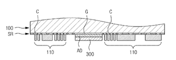
図1は、本発明の一実施例に係るパッケージ構造物を示す図であり、図2は、図1の一部を拡大した図である。 FIG. 1 is a diagram showing a package structure according to an embodiment of the present invention, and FIG. 2 is a partially enlarged diagram of FIG.
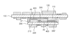
図1を参照すると、本発明の一実施例に係るパッケージ構造物は、第1基板100と、第2基板200と、インターポーザIPと、第1素子110と、補強材300と、第2素子210と、を含むことができる。
Referring to FIG. 1, a package structure according to an embodiment of the present invention includes a
第1基板100及び第2基板200は、電子素子が実装されて印刷回路基板としての実質的な役割を担い、インターポーザIPは、第1基板100と第2基板200とを上下に接続させ、第1基板100と第2基板200とはインターポーザIPで物理的に、電気的に接続される。
The
インターポーザIPは、絶縁層と貫通ビアを含むことができる。 The interposer IP can include insulating layers and through vias.
絶縁層は、単数または複数で形成されることができ、エポキシ樹脂、ポリイミド樹脂、BT樹脂等の絶縁物質で形成されることができる。具体的に、絶縁層は、PPG(prepreg)またはbuild up film(ex. Ajinomoto Build up Film)であり得る。この絶縁層は、繊維補強材、フィラー等を含むことができる。 The insulating layer may be formed of a single layer or a plurality of layers, and may be formed of an insulating material such as epoxy resin, polyimide resin, BT resin, or the like. Specifically, the insulating layer may be PPG (prepreg) or build up film (ex. Ajinomoto Build up Film). This insulating layer can include fiber reinforcements, fillers, and the like.
貫通ビアは、絶縁層を貫通し、インターポーザIPの上下面を接続する。インターポーザIPの上下面には、貫通ビアに接続される接続パッドが形成されることができる。この接続パッドは、第1基板100及び第2基板200に結合することができる。ここで、インターポーザIPは、ソルダー部材により第1基板100及び第2基板200に結合することができる。
The through via penetrates the insulating layer and connects the upper and lower surfaces of the interposer IP. Connection pads connected to the through vias may be formed on upper and lower surfaces of the interposer IP. The connection pads can be bonded to the
貫通ビアは、複数形成されることができ、複数の貫通ビアは、互いに離隔することができる。インターポーザIPは、内部に中空部を有するように環状に形成されることができる。この場合、複数の貫通ビアも環状のインターポーザIPに沿って、離隔して配置されることができる。 A plurality of through vias may be formed, and the plurality of through vias may be separated from each other. The interposer IP can be annularly formed to have a hollow inside. In this case, a plurality of through vias can also be spaced apart along the annular interposer IP.
第1基板100と第2基板200のそれぞれは、板状からなり、複数の絶縁材層と複数の回路層とで構成された多層基板であることができ、回路層を基準にして8層または10層の多層基板であることができる。
Each of the
第1基板100及び第2基板200の絶縁材層は、エポキシ樹脂、ポリイミド樹脂、BT樹脂、LCP(Liquid Crystal Polymer)等の絶縁物質で形成された層である。
The insulating material layers of the
回路層は、銅(Cu)のような金属等の伝導性物質で形成され、特定のパターンを有するように設計される。回路層は、絶縁材層の片面または両面に形成され、互いに異なる層の回路層は、絶縁材層を貫通するビア導体を介して電気的に接続されることができる。 The circuit layer is made of a conductive material such as a metal such as copper (Cu) and designed to have a specific pattern. A circuit layer is formed on one side or both sides of the insulating layer, and circuit layers in different layers can be electrically connected through via conductors penetrating the insulating layer.
第1基板100の一面には、第1素子110が実装される。ここで、第1基板100の一面は、第2基板200に向かい合う面である。第1素子110は、能動素子、受動素子、集積回路のうちの少なくとも1種であり、第1素子110は複数設けられることができ、複数の第1素子110は、能動素子、受動素子、集積回路のうちから多様に選択することができる。具体的に、第1素子110は、AP、Memory、BGA(Ball Grid Array)、CSP(Chip Scale Package)、LGA(Land Grid Array)等の多数の集積回路と、キャパシタ(capacitor)等の多数の受動素子と、を含むことができる。第1素子110は、ソルダー部材(図示せず)により第1基板100の表面に実装されることができる。
A
図2を参照すると、第1基板100の一面側の最外層の絶縁材層はソルダーレジストSRであり得る。すなわち、第1基板100の最外層には、ソルダーレジストSRが備えられることができる。この場合、ソルダーレジストSRは、第1基板100の回路層の一部を露出させながら回路層をカバーすることができる。特に、ソルダーレジストSRは、最外層の回路層をカバーする。最外層の回路層の一部は、有効な信号を伝達する信号伝逹回路Cであり、また他の一部は、グラウンドGであり得る。最外層の回路層のうちの信号伝逹回路Cの一部は、ソルダーレジストSRにより露出され、回路の露出された部分は、パッドとなり得る。ここで、ソルダーレジストSRには開口が形成され、最外層の回路層のうちの信号伝逹回路Cの一部は、ソルダーレジストSRの開口を介して露出される。
Referring to FIG. 2, the outermost insulation layer on one side of the
第1素子110は、ソルダー部材(図示せず)により上記パッドに実装されることができる。また、インターポーザIPも上記パッドに接合することができる。一方、グラウンドGもソルダーレジストSRによりカバーされ、グラウンドGの一部は、ソルダーレジストSRにより露出することができる。
The
インターポーザIPが内側に中空部を含む場合、第1素子110は、インターポーザIPの中空部内に位置することができる。ここで、インターポーザIPは、第1素子110を保護する機能をすることができる。
If the interposer IP includes a hollow inside, the
一方、第1基板100の他面には、第3素子120が実装されることができ、第3素子120は、複数設けられ、能動素子、受動素子、集積回路のうちから多様に選択することができる。第3素子120は、第1基板100の他面側の最外層の回路層に実装されることができる。第1素子110と第3素子120とは、第1基板100に形成された回路層及びビア導体を介して電気的に接続されることができる。
Meanwhile, the
再び、図1を参照すると、補強材300は、第1基板100の一面に付着され、第1基板100の反りを防止することができる。補強材300は、第1素子110から離隔する。
Referring to FIG. 1 again, the reinforcing
補強材300は、第1基板100の一面において第1素子110が実装された後の残った空間に形成されることができる。第1素子110が複数形成される場合、補強材300は、複数の第1素子110の間に形成され、すべての第1素子110から離隔することができる。補強材300は、第1素子110を取り囲むように形成されることができる。
The reinforcing
補強材300は、第1基板100の回路層に結合することができる。特に、補強材300は、第1基板100の一面側の最外層の回路層のうちのグラウンドGに結合することができる。すなわち、第1基板100の一面側の最外層の回路層のうちのグラウンドGの一部は、ソルダーレジストSRの開口により露出することができ、露出されたグラウンドGに補強材300が結合することができる。
The
補強材300は、第1基板100の反りを防止できるように、剛性が大きいか、歪み等の変形に耐える材質で形成することができる。補強材300は、インバー(invar)、SUS、タングステン、鉄、銅、アルミニウム等の金属で形成できるが、金属の種類が限定されることではない。一方、補強材300は、回路層よりも剛性の大きい金属を含む材質で形成されることができる。例えば、回路層は、銅で形成され、補強材300は、SUSで形成されることができる。
The reinforcing
また、補強材300は、ダイ(die)を含むことができる。ダイは、シリコンを含む材料で形成することができる。ここで、補強材300としてのダイは、ダミー(dummy)ダイであって、電子素子として機能するものではなくてもよい。すなわち、補強材300としてのダイは、第1基板100の一面側の最外層の回路層のうちの信号伝逹回路Cに電気的に接続されなくてもよい。一方、補強材300としてのダミーダイの厚さは、第1素子110の厚さよりも小さいことができる。
Also, the
補強材300は、接着部材ADで第1基板100の一面に付着されることができる。接着部材ADは、接着剤またはソルダーを含むことができる。すなわち、補強材300は、第1基板100の一面側のグラウンドGに接着剤またはソルダーで付着することができる。補強材300が金属である場合、接着剤が使用され、補強材300がダミーダイである場合、ソルダーが使用されることができるが、これに制限されない。
The reinforcing
具体的に、補強材300が金属である場合、第1基板100の一面に付着される補強材300の面は、平坦であることができ、補強材300と第1基板100の一面との間に接着剤が介在されることができる。接着剤は、液状タイプ、またはDAF(die attach film)、テープ等のフィルムタイプであり得る。接着剤の成分は、ポリウレタン、アクリル、EVA(ethylene co-vinyl acetate)、PVAc(polyvinyl acetate)等を含むことができるが、これらに制限されない。
Specifically, when the reinforcing
補強材300がダミーダイである場合、ダイは、複数の金属端子を含むことができ、金属端子には、ソルダーが結合され、ソルダーは、第1基板100の一面に結合することができる。特に、ソルダーは、第1基板100の一面側のソルダーレジストSRに直接付着されるよりも最外層の回路層のグラウンドGにさらに優れた密着力で付着されることができる。ただし、上述したように、補強材300がダミーダイである場合、必ずしもソルダーにより結合される必要はなく、接着剤により接着されることもできる。
When the
インターポーザIPが内側に中空部を含む場合、補強材300は、インターポーザIPの中空部内に位置することができる。
If the interposer IP includes a hollow inside, the reinforcing
第2基板200の一面には、第2素子210が実装される。ここで、第2基板200の一面は、第1基板100に向かい合う面である。特に、第2素子210は、補強材300の向かい側に配置される。これにより、第2素子210と補強材300とは、それぞれをいずれか1つの平面に投映したとき、重畳する領域が存在する。補強材300と第2素子210とは、印刷回路基板の厚さ方向(図面の上下方向)において互いに離隔することができる。
A
第2基板200の他面には、第4素子220が実装されることができる。この場合、第1基板100の2つの面と第2基板200の2つの面がすべて電子素子実装面として使用できるので、印刷回路基板としての使用面積が最大化することができる。
A
インターポーザIPが内側に中空部を含む場合、第2素子210は、インターポーザIPの中空部内に位置することができる。ここで、インターポーザIPは、第2素子210を保護する機能をすることができる。
If the interposer IP includes a hollow inside, the
本発明の一実施例に係るパッケージ構造物は、充填部材400をさらに含むことができる。
A package structure according to an embodiment of the present invention may further include a filling
充填部材400は、補強材300と第2素子210との間に介在され、補強材300及び第2素子210とそれぞれ接触する。上述したように、補強材300と第2素子210とは、上下方向において互いに離隔しており、離隔することにより形成された空間に充填部材400が形成できる。
The filling
充填部材400により、補強材300及び第2素子210が固定されることができ、これにより、第1基板100及び第2基板200の反りが効果的に低減することができる。
The reinforcing
充填部材400は、接着物質を含むことができ、ポリエステル、ポリウレタン、アクリル、EVA(ethylene co-vinyl acetate)、PVAc(polyvinyl acetate)等を含むことができる。
The
充填部材400は、第2素子210から発生する熱を放出、移動させることができるように、熱伝導素材(TIM、thermal interface material)を含むことができる。熱伝導素材は、空気よりも熱伝導率が50倍以上高いこともある。熱伝導素材(TIM、thermal interface material)は、サーマルコンパウンド(thermal compound)またはサーマルグリース(thermal grease)等のペーストからなることができる。サーマルコンパウンドまたはサーマルグリースは、シリコンを含むか、酸化アルミニウム(aluminium oxide)(Al2O3)、boron nitride(BN)、酸化亜鉛(zinc oxide)(ZnO)等のセラミック材を含むか、または金属(銅、銀等)粒子を含有するゲルを含むことができる。
The filling
熱伝導素材は、サーマルテープ(thermal tape)またはサーマルパッド(thermal pad)のように付着タイプであってもよく、これは補強材300と第2素子210との間に位置し、補強材300と第2素子210のそれぞれに付着されることができる。
The heat-conducting material may be of adhesive type, such as a thermal tape or thermal pad, which is located between the
充填部材400は補強材300と接触し、補強材300はグラウンドGと接触するので、第2素子210から発生する熱は、充填部材400、補強材300、グラウンドGを介して放出されることができる。
Since the
図3に示すように、インターポーザIPが内側に中空部を含む場合、充填部材400は、インターポーザIPの中空部全体を充填することができる。すなわち、充填部材400は、補強材300と第2素子210との間のみではなく、それ以外の領域も充填することができる。この場合、充填部材400の広い領域により、第1基板100及び第2基板200の反りが効果的に低減でき、充填部材400が熱伝導素材である場合は、充填部材400がサーマルコンパウンドまたはサーマルグリース等のペーストからなることができ、このように、充填部材400がインターポーザIPの中空部を充填すると、放熱效果も増大できる。ここで、充填部材400は、セラミック材を含む熱伝導素材であってもよい。
As shown in FIG. 3, when the interposer IP includes a hollow inside, the filling
一方、補強材は、第2基板200の一面にも形成されることができ、第2基板200の一面に形成された補強材300を第2の補強材300'と称し、上述した補強材300と区別する。第2の補強材300'は、第2基板200の反りを低減することができる。
Meanwhile, the reinforcing material may also be formed on one surface of the
第2の補強材300'は、第2素子210から離隔する。すなわち、第2の補強材300'は、第2基板200の一面に第2素子210が実装された後の残った空間に形成されることができ、第2素子210が複数である場合は、複数の第2素子210のすべてから離隔するように第2の補強材300'を形成することができる。第2の補強材300'は、第2素子210を取り囲むように形成されることができる。
The
第2の補強材300'は、第2基板200の回路層に結合することができる。特に、第2の補強材300'は、第2基板200の一面側の最外層の回路層のうちのグラウンドに結合することができる。すなわち、第2基板200の一面側の最外層の回路層のうちのグラウンドの一部は、ソルダーレジストの開口により露出することができ、露出されたグラウンドに第2の補強材300'が結合することができる。
A
第2の補強材300'は、接着部材ADにより第2基板200の一面に付着されることができる。接着部材ADは、接着剤またはソルダーを含むことができる。すなわち、第2の補強材300'は、第2基板200の一面側のグラウンドGに接着剤またはソルダーで付着されることができる。第2の補強材300'が金属である場合、液状タイプまたはフィルムタイプの接着剤が使用され、第2の補強材300'がダミーダイである場合、ソルダーを使用できるが、これに制限されない。
The second reinforcing member 300' may be attached to one surface of the
第2の補強材300'は、第2基板200の反りを防止できるように剛性が大きいか、歪み等の変形に耐える材質で形成することができる。第2の補強材300'は、インバー(invar)、SUS、タングステン、鉄、銅、アルミニウムなどの金属で形成することができるが、金属の種類に制限はない。
The second reinforcing
一方、第2の補強材300'は、回路層よりも剛性の大きい金属を含む材質で形成されることができる。例えば、回路層は、銅で形成され、第2の補強材300'は、SUSで形成されることができる。 On the other hand, the second reinforcing member 300' may be made of a material containing metal having higher rigidity than the circuit layer. For example, the circuit layer can be made of copper and the second stiffener 300' can be made of SUS.
また、第2の補強材300'は、ダイ(die)を含むことができる。ダイは、シリコンを含む材料で形成されることができる。ここで、第2の補強材300'としてのダイは、ダミー(dummy)ダイであって、電子素子として機能するものではなくてもよい。すなわち、第2の補強材300'としてのダイは、第2基板200の一面側の最外層の回路層のうちの信号伝逹回路Cに電気的に接続されなくてもよい。一方、補強材300としてのダミーダイの厚さは、第1素子110の厚さよりも小さいことができる。
Also, the second stiffener 300' may include a die. The die can be made of a material that includes silicon. Here, the die as the second reinforcing member 300' may be a dummy die and may not function as an electronic device. That is, the die as the second reinforcing
インターポーザIPが内側に中空部を含む場合、第2の補強材300'は、インターポーザIPの中空部内に位置することができる。 If the interposer IP includes a hollow inside, the second stiffener 300' can be located inside the hollow of the interposer IP.
第1基板100の一面に形成された第1素子110は、上記第2の補強材300'の向かい側に位置して互いに向かい合うことができ、第2の補強材300'と第1素子110 との間には、充填部材400が介在されることができる。すなわち、第2の補強材300'と第1素子110は、上下に離隔しており、充填部材400が第2の補強材300'と第1素子110との間に介在され、第2の補強材300及び第1素子110のそれぞれと接触することができる。充填部材400は、サーマルコンパウンドであってもよい。
The
その他に、上述した補強材300に関する説明を第2の補強材300'に同様に適用することができる。
In addition, the descriptions of the
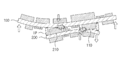
図4を参照すると、補強材300がない場合は、第1基板100及び第2基板200に反りが発生し、第1基板100及び第2基板200の反りにより、第2素子210が第1基板100にぶつかり、第1素子110が第2基板200にぶつかることがある。しかし、本発明によれば、補強材300が第1基板100及び第2基板200の反りを低減することができるので、充填部材400が素子と基板との衝突を防止することができる。
Referring to FIG. 4, if the reinforcing
以上、本発明の一実施例について説明したが、当該技術分野で通常の知識を有する者であれば、特許請求の範囲に記載された本発明の思想から逸脱しない範囲内で、構成要素の付加、変更、削除または追加等により本発明を多様に修正及び変更することができ、これも本発明の権利範囲内に含まれるものといえよう。 An embodiment of the present invention has been described above. However, those skilled in the art will be able to add components without departing from the spirit of the present invention described in the scope of claims. , alterations, deletions, additions, etc., can be variously modified and changed, which are also included in the scope of the invention.
100 第1基板
200 第2基板
IP インターポーザ
300、300' 補強材
400 充填部材
100
Claims (13)
前記第1基板の前記第2基板に向かい合う一面に実装された第1素子と、
前記第1基板の前記一面に、前記第1素子から離隔して付着される補強材と、
前記補強材の向かい側に位置するように、前記第2基板の一面に実装される第2素子と、を含むパッケージ構造物。 a first substrate and a second substrate vertically coupled with an interposer;
a first element mounted on one surface of the first substrate facing the second substrate;
a reinforcing material attached to the one surface of the first substrate and spaced apart from the first element;
a second element mounted on one surface of the second substrate opposite the stiffener.
前記第1素子、前記補強材及び前記第2素子は、前記中空部内に収容され、
前記充填部材が前記中空部を充填する請求項2又は3に記載のパッケージ構造物。 The interposer includes a hollow portion,
the first element, the reinforcing member and the second element are accommodated in the hollow portion;
4. A package structure according to claim 2 or 3, wherein said filling member fills said hollow portion.
前記第1素子、前記補強材及び前記第2素子は、前記中空部内に収容される請求項1~4の何れか一項に記載のパッケージ構造物。 The interposer includes a hollow portion,
5. The package structure according to any one of claims 1 to 4, wherein said first element, said reinforcing member and said second element are accommodated in said hollow portion.
前記ソルダーレジストは、前記第1基板の回路層を露出させ、
前記補強材が、露出された前記回路層に付着される請求項1~5の何れか一項に記載のパッケージ構造物。 The outermost layer of the first substrate is provided with a solder resist,
The solder resist exposes the circuit layer of the first substrate,
The package structure according to any one of claims 1 to 5, wherein the reinforcing material is attached to the exposed circuit layer.
前記補強材は、前記複数の第1素子の間に配置される請求項1~9の何れか一項に記載のパッケージ構造物。 The first element is composed of a plurality,
The package structure according to any one of claims 1 to 9, wherein the stiffener is arranged between the plurality of first elements.
前記第1素子と前記第2の補強材との間に介在され、前記第1素子及び前記第2の補強材のそれぞれと接触する充填部材をさらに含む請求項12に記載のパッケージ構造物。 the first element and the second stiffener are located opposite each other;
13. The package structure of claim 12, further comprising a filler member interposed between the first element and the second stiffener and in contact with each of the first element and the second stiffener.
Applications Claiming Priority (2)
| Application Number | Priority Date | Filing Date | Title |
|---|---|---|---|
| KR1020180139325A KR102561946B1 (en) | 2018-11-13 | 2018-11-13 | Package structure |
| KR10-2018-0139325 | 2018-11-13 |
Publications (2)
| Publication Number | Publication Date |
|---|---|
| JP2020080398A JP2020080398A (en) | 2020-05-28 |
| JP7200460B2 true JP7200460B2 (en) | 2023-01-10 |
Family
ID=70802507
Family Applications (1)
| Application Number | Title | Priority Date | Filing Date |
|---|---|---|---|
| JP2019100507A Active JP7200460B2 (en) | 2018-11-13 | 2019-05-29 | package structure |
Country Status (3)
| Country | Link |
|---|---|
| JP (1) | JP7200460B2 (en) |
| KR (1) | KR102561946B1 (en) |
| TW (1) | TWI793319B (en) |
Families Citing this family (1)
| Publication number | Priority date | Publication date | Assignee | Title |
|---|---|---|---|---|
| WO2025146949A1 (en) * | 2024-01-02 | 2025-07-10 | 삼성전자주식회사 | Electronic device comprising printed circuit board including thermal interface material |
Citations (8)
| Publication number | Priority date | Publication date | Assignee | Title |
|---|---|---|---|---|
| US20040089943A1 (en) | 2002-11-07 | 2004-05-13 | Masato Kirigaya | Electronic control device and method for manufacturing the same |
| JP2006173152A (en) | 2004-12-13 | 2006-06-29 | Matsushita Electric Ind Co Ltd | Relay board and three-dimensional wiring structure |
| JP2006210852A (en) | 2005-01-31 | 2006-08-10 | Toshiba Corp | Circuit board for mounting surface-mounted circuit components and manufacturing method thereof |
| JP2006261387A (en) | 2005-03-17 | 2006-09-28 | Matsushita Electric Ind Co Ltd | Module and its manufacturing method |
| JP2009176931A (en) | 2008-01-24 | 2009-08-06 | Panasonic Corp | Semiconductor device and electronic equipment |
| JP2013026346A (en) | 2011-07-19 | 2013-02-04 | Toshiba Corp | Semiconductor device |
| JP2014165481A (en) | 2013-02-28 | 2014-09-08 | Kyocer Slc Technologies Corp | Semiconductor device mounting body |
| US20180190622A1 (en) | 2014-03-07 | 2018-07-05 | Bridge Semiconductor Corporation | 3-d stacking semiconductor assembly having heat dissipation characteristics |
Family Cites Families (9)
| Publication number | Priority date | Publication date | Assignee | Title |
|---|---|---|---|---|
| JP2004158700A (en) | 2002-11-07 | 2004-06-03 | Denso Corp | Electronic control device and method of manufacturing the same |
| TWI460844B (en) * | 2009-04-06 | 2014-11-11 | 金龍國際公司 | Stacked package structure with embedded wafer and germanium via film and manufacturing method thereof |
| US8247900B2 (en) * | 2009-12-29 | 2012-08-21 | Taiwan Semiconductor Manufacturing Company, Ltd. | Flip chip package having enhanced thermal and mechanical performance |
| TW201314935A (en) * | 2011-09-23 | 2013-04-01 | Mke Technology Co Ltd | Solar cell package structure |
| KR20150009728A (en) * | 2013-07-17 | 2015-01-27 | 삼성전기주식회사 | Electric component module package and mounting structrue threrof |
| KR101324595B1 (en) | 2013-08-07 | 2013-11-01 | (주)드림텍 | Main board for mobil terminal with excellent assembling and mobility |
| JP2016025143A (en) | 2014-07-17 | 2016-02-08 | イビデン株式会社 | Circuit board and manufacturing method of the same |
| JP2016173152A (en) | 2015-03-17 | 2016-09-29 | Ntn株式会社 | Cage and rolling bearing |
| DE112016007565T5 (en) | 2016-12-30 | 2019-10-02 | Intel Corporation | MICROELECTRONIC COMPONENTS DESIGNED WITH 3D STACKED, ULTRADOUND HOUSING MODULES FOR HIGH FREQUENCY COMMUNICATIONS |
-
2018
- 2018-11-13 KR KR1020180139325A patent/KR102561946B1/en active Active
-
2019
- 2019-05-08 TW TW108115817A patent/TWI793319B/en active
- 2019-05-29 JP JP2019100507A patent/JP7200460B2/en active Active
Patent Citations (8)
| Publication number | Priority date | Publication date | Assignee | Title |
|---|---|---|---|---|
| US20040089943A1 (en) | 2002-11-07 | 2004-05-13 | Masato Kirigaya | Electronic control device and method for manufacturing the same |
| JP2006173152A (en) | 2004-12-13 | 2006-06-29 | Matsushita Electric Ind Co Ltd | Relay board and three-dimensional wiring structure |
| JP2006210852A (en) | 2005-01-31 | 2006-08-10 | Toshiba Corp | Circuit board for mounting surface-mounted circuit components and manufacturing method thereof |
| JP2006261387A (en) | 2005-03-17 | 2006-09-28 | Matsushita Electric Ind Co Ltd | Module and its manufacturing method |
| JP2009176931A (en) | 2008-01-24 | 2009-08-06 | Panasonic Corp | Semiconductor device and electronic equipment |
| JP2013026346A (en) | 2011-07-19 | 2013-02-04 | Toshiba Corp | Semiconductor device |
| JP2014165481A (en) | 2013-02-28 | 2014-09-08 | Kyocer Slc Technologies Corp | Semiconductor device mounting body |
| US20180190622A1 (en) | 2014-03-07 | 2018-07-05 | Bridge Semiconductor Corporation | 3-d stacking semiconductor assembly having heat dissipation characteristics |
Also Published As
| Publication number | Publication date |
|---|---|
| KR102561946B1 (en) | 2023-08-01 |
| JP2020080398A (en) | 2020-05-28 |
| KR20200055555A (en) | 2020-05-21 |
| TW202018881A (en) | 2020-05-16 |
| TWI793319B (en) | 2023-02-21 |
Similar Documents
| Publication | Publication Date | Title |
|---|---|---|
| US7242092B2 (en) | Substrate assembly with direct electrical connection as a semiconductor package | |
| US6525942B2 (en) | Heat dissipation ball grid array package | |
| CN101159254B (en) | Semiconductor device | |
| KR101476385B1 (en) | Mountable integrated circuit package-in-package system having adhesive spacing structures | |
| JP3110922B2 (en) | Multi-chip module | |
| US8553420B2 (en) | Enhanced stacked microelectronic assemblies with central contacts and improved thermal characteristics | |
| US8263871B2 (en) | Mount board and semiconductor module | |
| US8304922B2 (en) | Semiconductor package system with thermal die bonding | |
| TWI778236B (en) | semiconductor device | |
| JP5413971B2 (en) | Electronic component mounting apparatus and manufacturing method thereof | |
| KR100698526B1 (en) | A wiring board having a heat dissipation layer and a semiconductor package using the same | |
| US8970044B2 (en) | Integrated circuit packaging system with vertical interconnects and method of manufacture thereof | |
| KR20140057982A (en) | Semiconductor package and method of manufacturing the semiconductor package | |
| KR100768998B1 (en) | Chip Assembly Module of Bump Connection Type Using a Multi-layer Printed Circuit Substrate | |
| CN120432448B (en) | IC packaging structure and packaging method | |
| JP7200460B2 (en) | package structure | |
| TWI391084B (en) | Pcb structure having heat-dissipating member | |
| JP4627323B2 (en) | Semiconductor device | |
| JP4919689B2 (en) | Module board | |
| JP3024596B2 (en) | BGA type semiconductor device using film carrier tape | |
| KR20210035027A (en) | Electronic component module and manufacturing method thereof | |
| US20250379113A1 (en) | Semiconductor package and manufacturing method thereof | |
| JP3965867B2 (en) | Semiconductor package | |
| CN100505227C (en) | Substrate structure for direct electrical connection of semiconductor package | |
| JP2904754B2 (en) | Wiring board for mounting electronic components |
Legal Events
| Date | Code | Title | Description |
|---|---|---|---|
| A621 | Written request for application examination |
Free format text: JAPANESE INTERMEDIATE CODE: A621 Effective date: 20211104 |
|
| A977 | Report on retrieval |
Free format text: JAPANESE INTERMEDIATE CODE: A971007 Effective date: 20221110 |
|
| TRDD | Decision of grant or rejection written | ||
| A01 | Written decision to grant a patent or to grant a registration (utility model) |
Free format text: JAPANESE INTERMEDIATE CODE: A01 Effective date: 20221122 |
|
| A61 | First payment of annual fees (during grant procedure) |
Free format text: JAPANESE INTERMEDIATE CODE: A61 Effective date: 20221130 |
|
| R150 | Certificate of patent or registration of utility model |
Ref document number: 7200460 Country of ref document: JP Free format text: JAPANESE INTERMEDIATE CODE: R150 |
|
| R250 | Receipt of annual fees |
Free format text: JAPANESE INTERMEDIATE CODE: R250 |