JP7202802B2 - Semiconductor device manufacturing method - Google Patents
Semiconductor device manufacturing method Download PDFInfo
- Publication number
- JP7202802B2 JP7202802B2 JP2018138721A JP2018138721A JP7202802B2 JP 7202802 B2 JP7202802 B2 JP 7202802B2 JP 2018138721 A JP2018138721 A JP 2018138721A JP 2018138721 A JP2018138721 A JP 2018138721A JP 7202802 B2 JP7202802 B2 JP 7202802B2
- Authority
- JP
- Japan
- Prior art keywords
- resin layer
- adhesive resin
- adhesive
- semiconductor device
- manufacturing
- Prior art date
- Legal status (The legal status is an assumption and is not a legal conclusion. Google has not performed a legal analysis and makes no representation as to the accuracy of the status listed.)
- Active
Links
Images
Classifications
-
- H—ELECTRICITY
- H10—SEMICONDUCTOR DEVICES; ELECTRIC SOLID-STATE DEVICES NOT OTHERWISE PROVIDED FOR
- H10P—GENERIC PROCESSES OR APPARATUS FOR THE MANUFACTURE OR TREATMENT OF DEVICES COVERED BY CLASS H10
- H10P72/00—Handling or holding of wafers, substrates or devices during manufacture or treatment thereof
- H10P72/70—Handling or holding of wafers, substrates or devices during manufacture or treatment thereof for supporting or gripping
- H10P72/74—Handling or holding of wafers, substrates or devices during manufacture or treatment thereof for supporting or gripping using temporarily an auxiliary support
-
- H—ELECTRICITY
- H10—SEMICONDUCTOR DEVICES; ELECTRIC SOLID-STATE DEVICES NOT OTHERWISE PROVIDED FOR
- H10P—GENERIC PROCESSES OR APPARATUS FOR THE MANUFACTURE OR TREATMENT OF DEVICES COVERED BY CLASS H10
- H10P72/00—Handling or holding of wafers, substrates or devices during manufacture or treatment thereof
- H10P72/04—Apparatus for manufacture or treatment
- H10P72/0442—Apparatus for placing on an insulating substrate, e.g. tape
-
- C—CHEMISTRY; METALLURGY
- C09—DYES; PAINTS; POLISHES; NATURAL RESINS; ADHESIVES; COMPOSITIONS NOT OTHERWISE PROVIDED FOR; APPLICATIONS OF MATERIALS NOT OTHERWISE PROVIDED FOR
- C09J—ADHESIVES; NON-MECHANICAL ASPECTS OF ADHESIVE PROCESSES IN GENERAL; ADHESIVE PROCESSES NOT PROVIDED FOR ELSEWHERE; USE OF MATERIALS AS ADHESIVES
- C09J7/00—Adhesives in the form of films or foils
- C09J7/20—Adhesives in the form of films or foils characterised by their carriers
- C09J7/29—Laminated material
-
- C—CHEMISTRY; METALLURGY
- C09—DYES; PAINTS; POLISHES; NATURAL RESINS; ADHESIVES; COMPOSITIONS NOT OTHERWISE PROVIDED FOR; APPLICATIONS OF MATERIALS NOT OTHERWISE PROVIDED FOR
- C09J—ADHESIVES; NON-MECHANICAL ASPECTS OF ADHESIVE PROCESSES IN GENERAL; ADHESIVE PROCESSES NOT PROVIDED FOR ELSEWHERE; USE OF MATERIALS AS ADHESIVES
- C09J11/00—Features of adhesives not provided for in group C09J9/00, e.g. additives
- C09J11/02—Non-macromolecular additives
-
- C—CHEMISTRY; METALLURGY
- C09—DYES; PAINTS; POLISHES; NATURAL RESINS; ADHESIVES; COMPOSITIONS NOT OTHERWISE PROVIDED FOR; APPLICATIONS OF MATERIALS NOT OTHERWISE PROVIDED FOR
- C09J—ADHESIVES; NON-MECHANICAL ASPECTS OF ADHESIVE PROCESSES IN GENERAL; ADHESIVE PROCESSES NOT PROVIDED FOR ELSEWHERE; USE OF MATERIALS AS ADHESIVES
- C09J133/00—Adhesives based on homopolymers or copolymers of compounds having one or more unsaturated aliphatic radicals, each having only one carbon-to-carbon double bond, and at least one being terminated by only one carboxyl radical, or of salts, anhydrides, esters, amides, imides, or nitriles thereof; Adhesives based on derivatives of such polymers
- C09J133/04—Homopolymers or copolymers of esters
- C09J133/06—Homopolymers or copolymers of esters of esters containing only carbon, hydrogen and oxygen, the oxygen atom being present only as part of the carboxyl radical
- C09J133/08—Homopolymers or copolymers of acrylic acid esters
-
- C—CHEMISTRY; METALLURGY
- C09—DYES; PAINTS; POLISHES; NATURAL RESINS; ADHESIVES; COMPOSITIONS NOT OTHERWISE PROVIDED FOR; APPLICATIONS OF MATERIALS NOT OTHERWISE PROVIDED FOR
- C09J—ADHESIVES; NON-MECHANICAL ASPECTS OF ADHESIVE PROCESSES IN GENERAL; ADHESIVE PROCESSES NOT PROVIDED FOR ELSEWHERE; USE OF MATERIALS AS ADHESIVES
- C09J199/00—Adhesives based on natural macromolecular compounds or on derivatives thereof, not provided for in groups C09J101/00 -C09J107/00 or C09J189/00 - C09J197/00
-
- C—CHEMISTRY; METALLURGY
- C09—DYES; PAINTS; POLISHES; NATURAL RESINS; ADHESIVES; COMPOSITIONS NOT OTHERWISE PROVIDED FOR; APPLICATIONS OF MATERIALS NOT OTHERWISE PROVIDED FOR
- C09J—ADHESIVES; NON-MECHANICAL ASPECTS OF ADHESIVE PROCESSES IN GENERAL; ADHESIVE PROCESSES NOT PROVIDED FOR ELSEWHERE; USE OF MATERIALS AS ADHESIVES
- C09J7/00—Adhesives in the form of films or foils
- C09J7/20—Adhesives in the form of films or foils characterised by their carriers
-
- C—CHEMISTRY; METALLURGY
- C09—DYES; PAINTS; POLISHES; NATURAL RESINS; ADHESIVES; COMPOSITIONS NOT OTHERWISE PROVIDED FOR; APPLICATIONS OF MATERIALS NOT OTHERWISE PROVIDED FOR
- C09J—ADHESIVES; NON-MECHANICAL ASPECTS OF ADHESIVE PROCESSES IN GENERAL; ADHESIVE PROCESSES NOT PROVIDED FOR ELSEWHERE; USE OF MATERIALS AS ADHESIVES
- C09J9/00—Adhesives characterised by their physical nature or the effects produced, e.g. glue sticks
- C09J9/02—Electrically-conducting adhesives
-
- H—ELECTRICITY
- H10—SEMICONDUCTOR DEVICES; ELECTRIC SOLID-STATE DEVICES NOT OTHERWISE PROVIDED FOR
- H10P—GENERIC PROCESSES OR APPARATUS FOR THE MANUFACTURE OR TREATMENT OF DEVICES COVERED BY CLASS H10
- H10P52/00—Grinding, lapping or polishing of wafers, substrates or parts of devices
-
- H—ELECTRICITY
- H10—SEMICONDUCTOR DEVICES; ELECTRIC SOLID-STATE DEVICES NOT OTHERWISE PROVIDED FOR
- H10P—GENERIC PROCESSES OR APPARATUS FOR THE MANUFACTURE OR TREATMENT OF DEVICES COVERED BY CLASS H10
- H10P52/00—Grinding, lapping or polishing of wafers, substrates or parts of devices
- H10P52/40—Chemomechanical polishing [CMP]
- H10P52/402—Chemomechanical polishing [CMP] of semiconductor materials
-
- H—ELECTRICITY
- H10—SEMICONDUCTOR DEVICES; ELECTRIC SOLID-STATE DEVICES NOT OTHERWISE PROVIDED FOR
- H10P—GENERIC PROCESSES OR APPARATUS FOR THE MANUFACTURE OR TREATMENT OF DEVICES COVERED BY CLASS H10
- H10P72/00—Handling or holding of wafers, substrates or devices during manufacture or treatment thereof
- H10P72/70—Handling or holding of wafers, substrates or devices during manufacture or treatment thereof for supporting or gripping
- H10P72/74—Handling or holding of wafers, substrates or devices during manufacture or treatment thereof for supporting or gripping using temporarily an auxiliary support
- H10P72/7402—Wafer tapes, e.g. grinding or dicing support tapes
-
- H—ELECTRICITY
- H10—SEMICONDUCTOR DEVICES; ELECTRIC SOLID-STATE DEVICES NOT OTHERWISE PROVIDED FOR
- H10P—GENERIC PROCESSES OR APPARATUS FOR THE MANUFACTURE OR TREATMENT OF DEVICES COVERED BY CLASS H10
- H10P72/00—Handling or holding of wafers, substrates or devices during manufacture or treatment thereof
- H10P72/70—Handling or holding of wafers, substrates or devices during manufacture or treatment thereof for supporting or gripping
- H10P72/74—Handling or holding of wafers, substrates or devices during manufacture or treatment thereof for supporting or gripping using temporarily an auxiliary support
- H10P72/7402—Wafer tapes, e.g. grinding or dicing support tapes
- H10P72/7404—Wafer tapes, e.g. grinding or dicing support tapes the wafer tape being a laminate of three or more layers, e.g. including additional layers beyond a base layer and an uppermost adhesive layer
-
- C—CHEMISTRY; METALLURGY
- C08—ORGANIC MACROMOLECULAR COMPOUNDS; THEIR PREPARATION OR CHEMICAL WORKING-UP; COMPOSITIONS BASED THEREON
- C08K—Use of inorganic or non-macromolecular organic substances as compounding ingredients
- C08K2201/00—Specific properties of additives
- C08K2201/001—Conductive additives
-
- C—CHEMISTRY; METALLURGY
- C09—DYES; PAINTS; POLISHES; NATURAL RESINS; ADHESIVES; COMPOSITIONS NOT OTHERWISE PROVIDED FOR; APPLICATIONS OF MATERIALS NOT OTHERWISE PROVIDED FOR
- C09J—ADHESIVES; NON-MECHANICAL ASPECTS OF ADHESIVE PROCESSES IN GENERAL; ADHESIVE PROCESSES NOT PROVIDED FOR ELSEWHERE; USE OF MATERIALS AS ADHESIVES
- C09J2203/00—Applications of adhesives in processes or use of adhesives in the form of films or foils
- C09J2203/326—Applications of adhesives in processes or use of adhesives in the form of films or foils for bonding electronic components such as wafers, chips or semiconductors
-
- C—CHEMISTRY; METALLURGY
- C09—DYES; PAINTS; POLISHES; NATURAL RESINS; ADHESIVES; COMPOSITIONS NOT OTHERWISE PROVIDED FOR; APPLICATIONS OF MATERIALS NOT OTHERWISE PROVIDED FOR
- C09J—ADHESIVES; NON-MECHANICAL ASPECTS OF ADHESIVE PROCESSES IN GENERAL; ADHESIVE PROCESSES NOT PROVIDED FOR ELSEWHERE; USE OF MATERIALS AS ADHESIVES
- C09J2301/00—Additional features of adhesives in the form of films or foils
- C09J2301/30—Additional features of adhesives in the form of films or foils characterized by the chemical, physicochemical or physical properties of the adhesive or the carrier
- C09J2301/312—Additional features of adhesives in the form of films or foils characterized by the chemical, physicochemical or physical properties of the adhesive or the carrier parameters being the characterizing feature
-
- C—CHEMISTRY; METALLURGY
- C09—DYES; PAINTS; POLISHES; NATURAL RESINS; ADHESIVES; COMPOSITIONS NOT OTHERWISE PROVIDED FOR; APPLICATIONS OF MATERIALS NOT OTHERWISE PROVIDED FOR
- C09J—ADHESIVES; NON-MECHANICAL ASPECTS OF ADHESIVE PROCESSES IN GENERAL; ADHESIVE PROCESSES NOT PROVIDED FOR ELSEWHERE; USE OF MATERIALS AS ADHESIVES
- C09J2301/00—Additional features of adhesives in the form of films or foils
- C09J2301/40—Additional features of adhesives in the form of films or foils characterized by the presence of essential components
- C09J2301/408—Additional features of adhesives in the form of films or foils characterized by the presence of essential components additives as essential feature of the adhesive layer
-
- C—CHEMISTRY; METALLURGY
- C09—DYES; PAINTS; POLISHES; NATURAL RESINS; ADHESIVES; COMPOSITIONS NOT OTHERWISE PROVIDED FOR; APPLICATIONS OF MATERIALS NOT OTHERWISE PROVIDED FOR
- C09J—ADHESIVES; NON-MECHANICAL ASPECTS OF ADHESIVE PROCESSES IN GENERAL; ADHESIVE PROCESSES NOT PROVIDED FOR ELSEWHERE; USE OF MATERIALS AS ADHESIVES
- C09J2301/00—Additional features of adhesives in the form of films or foils
- C09J2301/40—Additional features of adhesives in the form of films or foils characterized by the presence of essential components
- C09J2301/416—Additional features of adhesives in the form of films or foils characterized by the presence of essential components use of irradiation
-
- H—ELECTRICITY
- H10—SEMICONDUCTOR DEVICES; ELECTRIC SOLID-STATE DEVICES NOT OTHERWISE PROVIDED FOR
- H10P—GENERIC PROCESSES OR APPARATUS FOR THE MANUFACTURE OR TREATMENT OF DEVICES COVERED BY CLASS H10
- H10P72/00—Handling or holding of wafers, substrates or devices during manufacture or treatment thereof
- H10P72/70—Handling or holding of wafers, substrates or devices during manufacture or treatment thereof for supporting or gripping
- H10P72/74—Handling or holding of wafers, substrates or devices during manufacture or treatment thereof for supporting or gripping using temporarily an auxiliary support
- H10P72/7416—Handling or holding of wafers, substrates or devices during manufacture or treatment thereof for supporting or gripping using temporarily an auxiliary support used during dicing or grinding
-
- H—ELECTRICITY
- H10—SEMICONDUCTOR DEVICES; ELECTRIC SOLID-STATE DEVICES NOT OTHERWISE PROVIDED FOR
- H10P—GENERIC PROCESSES OR APPARATUS FOR THE MANUFACTURE OR TREATMENT OF DEVICES COVERED BY CLASS H10
- H10P72/00—Handling or holding of wafers, substrates or devices during manufacture or treatment thereof
- H10P72/70—Handling or holding of wafers, substrates or devices during manufacture or treatment thereof for supporting or gripping
- H10P72/74—Handling or holding of wafers, substrates or devices during manufacture or treatment thereof for supporting or gripping using temporarily an auxiliary support
- H10P72/7422—Handling or holding of wafers, substrates or devices during manufacture or treatment thereof for supporting or gripping using temporarily an auxiliary support used to protect an active side of a device or wafer
-
- H—ELECTRICITY
- H10—SEMICONDUCTOR DEVICES; ELECTRIC SOLID-STATE DEVICES NOT OTHERWISE PROVIDED FOR
- H10P—GENERIC PROCESSES OR APPARATUS FOR THE MANUFACTURE OR TREATMENT OF DEVICES COVERED BY CLASS H10
- H10P72/00—Handling or holding of wafers, substrates or devices during manufacture or treatment thereof
- H10P72/70—Handling or holding of wafers, substrates or devices during manufacture or treatment thereof for supporting or gripping
- H10P72/74—Handling or holding of wafers, substrates or devices during manufacture or treatment thereof for supporting or gripping using temporarily an auxiliary support
- H10P72/744—Details of chemical or physical process used for separating the auxiliary support from a device or a wafer
-
- H—ELECTRICITY
- H10—SEMICONDUCTOR DEVICES; ELECTRIC SOLID-STATE DEVICES NOT OTHERWISE PROVIDED FOR
- H10W—GENERIC PACKAGES, INTERCONNECTIONS, CONNECTORS OR OTHER CONSTRUCTIONAL DETAILS OF DEVICES COVERED BY CLASS H10
- H10W72/00—Interconnections or connectors in packages
- H10W72/01—Manufacture or treatment
- H10W72/012—Manufacture or treatment of bump connectors, dummy bumps or thermal bumps
- H10W72/01204—Manufacture or treatment of bump connectors, dummy bumps or thermal bumps using temporary auxiliary members, e.g. using sacrificial coatings or handle substrates
-
- H—ELECTRICITY
- H10—SEMICONDUCTOR DEVICES; ELECTRIC SOLID-STATE DEVICES NOT OTHERWISE PROVIDED FOR
- H10W—GENERIC PACKAGES, INTERCONNECTIONS, CONNECTORS OR OTHER CONSTRUCTIONAL DETAILS OF DEVICES COVERED BY CLASS H10
- H10W72/00—Interconnections or connectors in packages
- H10W72/20—Bump connectors, e.g. solder bumps or copper pillars; Dummy bumps; Thermal bumps
- H10W72/251—Materials
- H10W72/252—Materials comprising solid metals or solid metalloids, e.g. PbSn, Ag or Cu
Landscapes
- Chemical & Material Sciences (AREA)
- Organic Chemistry (AREA)
- Mechanical Treatment Of Semiconductor (AREA)
- Adhesive Tapes (AREA)
- Adhesives Or Adhesive Processes (AREA)
Description
本発明は、半導体装置の製造方法に関する。 The present invention relates to a method of manufacturing a semiconductor device.
半導体装置の製造工程の中で、半導体ウェハを研削する工程においては、半導体ウェハの損傷を防止するために、半導体ウェハに粘着性フィルムが貼り付けられる。
このような粘着性フィルムには、一般的に、基材フィルムに紫外線硬化型の粘着性樹脂層を積層させたフィルムが用いられている。この粘着性フィルムは紫外線を照射することで、粘着性樹脂層が架橋して粘着性樹脂層の粘着力が低下するため、半導体ウェハから粘着性フィルムを容易に剥離することができる。
2. Description of the Related Art In the process of grinding a semiconductor wafer in the manufacturing process of a semiconductor device, an adhesive film is attached to the semiconductor wafer in order to prevent the semiconductor wafer from being damaged.
As such an adhesive film, a film obtained by laminating an ultraviolet curable adhesive resin layer on a base film is generally used. By irradiating the adhesive film with ultraviolet rays, the adhesive resin layer is crosslinked and the adhesive strength of the adhesive resin layer is lowered, so that the adhesive film can be easily peeled off from the semiconductor wafer.
一方で、このような粘着性フィルムを用いた半導体装置の製造工程では、半導体ウェハから粘着性フィルムを剥離する際に剥離帯電と呼ばれる静電気が発生してしまう場合があった。このようにして生じた静電気によって半導体ウェハに形成した回路が破壊されたり(静電破壊)、半導体ウェハに形成した回路へ埃等の異物が付着してしまったりする場合があった。
特に、近年の半導体ウェハの高密度化・配線の狭ピッチ化に伴って、半導体ウェハはこれまで以上に静電気による影響を受けやすくなってきている傾向にある。
こうした事情に鑑みて、近年、半導体装置の製造工程において半導体ウェハの損傷の防止のために使用する粘着性フィルムについても、帯電防止性能をさらに向上させることが要求されている。
On the other hand, in the manufacturing process of a semiconductor device using such an adhesive film, static electricity called peeling electrification may be generated when the adhesive film is peeled off from the semiconductor wafer. The static electricity generated in this way may destroy circuits formed on the semiconductor wafer (electrostatic breakdown), or foreign matter such as dust may adhere to the circuits formed on the semiconductor wafer.
In particular, as the density of semiconductor wafers increases and the pitch of wiring becomes narrower in recent years, semiconductor wafers tend to be more easily affected by static electricity than ever before.
In view of these circumstances, in recent years, it has been required to further improve the antistatic performance of adhesive films used for preventing damage to semiconductor wafers in the manufacturing process of semiconductor devices.
このような半導体ウェハ加工用粘着性フィルムに関する技術としては、例えば、特許文献1(特開2011-210944号公報)に記載のものが挙げられる。 Techniques related to such adhesive films for semiconductor wafer processing include, for example, those described in Patent Document 1 (Japanese Patent Application Laid-Open No. 2011-210944).
特許文献1には、基材フィルムと光硬化型の粘着剤層から構成される粘着テープであって、上記基材フィルムの少なくとも片面に導電性高分子を含有する帯電防止層、上記帯電防止層上にベースポリマーの分子内に光硬化性不飽和炭素結合を含有する粘着剤層を有し、紫外線硬化前後の上記粘着剤層側の表面抵抗率が1×10⁶~5×10¹²Ω/□であり、粘着剤層の厚みが20~250μmであり、粘着テープをシリコンミラーウェハに貼合した場合の粘着剤層の紫外線硬化後の90度引き剥がし粘着力(JIS Z 0237に準拠;剥離速度は50mm/min)が、0.15~0.25N/25mmであることを特徴とする帯電防止性半導体加工用粘着テープが記載されている。 Patent Document 1 discloses an adhesive tape composed of a base film and a photocurable adhesive layer, an antistatic layer containing a conductive polymer on at least one side of the base film, the antistatic layer It has an adhesive layer containing a photocurable unsaturated carbon bond in the molecule of the base polymer thereon, and the surface resistivity of the adhesive layer side before and after UV curing is 1×10 6 to 5×10 12 Ω/. □, the thickness of the adhesive layer is 20 to 250 μm, and the 90 degree peeling adhesive strength after UV curing of the adhesive layer when the adhesive tape is laminated to a silicon mirror wafer (based on JIS Z 0237; peeling It describes an antistatic pressure-sensitive adhesive tape for semiconductor processing, characterized in that the speed is 50 mm/min) and the speed is 0.15 to 0.25 N/25 mm.
上記背景技術の項に前述したように、近年、半導体ウェハ加工用粘着性フィルムの静電気対策という観点について要求される技術水準は、ますます高くなっている。
本発明者らの検討によれば、特許文献1に記載されているような、基材フィルムと帯電防止層と粘着剤層とがこの順番に積層された粘着性フィルムにおいて、帯電防止性が十分に満足するものではないことが明らかになった。
より具体的には、特許文献1に記載されているような粘着性フィルムは、紫外線硬化後に粘着剤層の飽和帯電圧が大幅に増加し、帯電防止性が大きく悪化してしまうことが明らかになった。
As described above in the Background Art section, in recent years, the technical level required from the standpoint of countermeasures against static electricity in adhesive films for processing semiconductor wafers is becoming higher and higher.
According to the studies of the present inventors, the adhesive film in which the base film, the antistatic layer and the adhesive layer are laminated in this order, as described in Patent Document 1, has sufficient antistatic properties. was found to be unsatisfactory.
More specifically, it is clear that the adhesive film described in Patent Document 1 significantly increases the saturation voltage of the adhesive layer after UV curing, and greatly deteriorates the antistatic property. became.
本発明は上記事情に鑑みてなされたものであり、半導体ウェハの研削を安定的におこなうことができるとともに回路の絶縁破壊を抑制でき、品質に優れた半導体装置を安定的に得ることが可能な半導体装置の製造方法を提供するものである。 The present invention has been made in view of the above circumstances, and can stably grind a semiconductor wafer, suppress dielectric breakdown of a circuit, and stably obtain a semiconductor device of excellent quality. A method of manufacturing a semiconductor device is provided.
本発明者らは、上記課題を達成するために鋭意検討を重ねた。その結果、粘着性フィルムの層構成を、基材層と、帯電防止層と、導電性添加剤を含む粘着性樹脂層と、をこの順番に備える層構成とすることにより、紫外線硬化後の粘着性フィルムの飽和帯電圧の上昇を抑制できることを見出して、本発明を完成させた。 The inventors of the present invention have made extensive studies in order to achieve the above object. As a result, by making the layer structure of the adhesive film into a layer structure comprising a substrate layer, an antistatic layer, and an adhesive resin layer containing a conductive additive in this order, the adhesive after UV curing can be obtained. The inventors have found that it is possible to suppress the increase in the saturation charge voltage of a flexible film, and completed the present invention.
本発明によれば、以下に示す半導体装置の製造方法が提供される。 According to the present invention, a method for manufacturing a semiconductor device as described below is provided.
[1]
回路形成面を有する半導体ウェハと、上記半導体ウェハの上記回路形成面側に貼り合わされた粘着性フィルムと、を備える構造体を準備する工程(A)と、
上記半導体ウェハの上記回路形成面側とは反対側の面をバックグラインドする工程(B)と、
上記粘着性フィルムに紫外線を照射した後に上記半導体ウェハから上記粘着性フィルムを除去する工程(C)と、
を少なくとも備える半導体装置の製造方法であって、
上記粘着性フィルムとして、
基材層と、帯電防止層と、導電性添加剤を含む粘着性樹脂層と、をこの順番に備え、上記粘着性樹脂層が上記半導体ウェハの上記回路形成面側となるように用いる粘着性フィルムを使用する半導体装置の製造方法。
[2]
上記[1]に記載の半導体装置の製造方法において、
上記半導体ウェハの上記回路形成面にはバンプ電極が形成されている半導体装置の製造方法。
[3]
上記[1]または[2]に記載の半導体装置の製造方法において、
上記粘着性樹脂層は紫外線硬化型粘着性樹脂を含む半導体装置の製造方法。
[4]
上記[3]に記載の半導体装置の製造方法において、
上記粘着性樹脂層における上記導電性添加剤の含有量が、上記紫外線硬化型粘着性樹脂100質量部に対し、0.01質量部以上10質量部以下である半導体装置の製造方法。
[5]
上記[1]乃至[4]いずれか一つに記載の半導体装置の製造方法において、
上記導電性添加剤はカチオン性界面活性剤、アニオン性界面活性剤、ノニオン性界面活性剤、両性界面活性剤、およびイオン液体から選択される一種または二種以上を含む半導体装置の製造方法。
[6]
上記[1]乃至[5]いずれか一つに記載の半導体装置の製造方法において、
上記粘着性樹脂層の厚みが5μm以上550μm以下である半導体装置の製造方法。
[7]
上記[1]乃至[6]いずれか一つに記載の半導体装置の製造方法において、
上記帯電防止層は導電性高分子を含む半導体装置の製造方法。
[8]
上記[1]乃至[7]いずれか一つに記載の半導体装置の製造方法において、
上記基材層と上記帯電防止層との間に凹凸吸収性樹脂層をさらに備える半導体装置の製造方法。
[9]
上記[1]乃至[8]いずれか一つに記載の半導体装置の製造方法において、
上記工程(C)では、上記粘着性フィルムに対し、300mJ/cm2以上の線量の紫外線を照射することによって、上記粘着性樹脂層を光硬化させて上記粘着性樹脂層の粘着力を低下させた後に、上記半導体ウェハから上記粘着性フィルムを除去する半導体装置の製造方法。
[10]
上記[1]乃至[9]いずれか一つに記載の半導体装置の製造方法において、
下記の方法で測定される、紫外線硬化後の上記粘着性樹脂層表面の飽和帯電圧V1が1.0kV以下である半導体装置の製造方法。
(方法)
上記粘着性樹脂層に対し、25℃の環境下で高圧水銀ランプを用いて主波長365nmの紫外線を照射強度100mW/cm2で紫外線量1080mJ/cm2照射して上記粘着性樹脂層を光硬化させる。次いで、印加電圧10kV、試料と電極との距離20mm、25℃、50%RHの条件下で上記粘着性樹脂層の表面に電圧の印加を30秒おこない、JIS L1094に準じて上記粘着性樹脂層の表面の飽和帯電圧(V1)を算出する。
[11]
上記[1]乃至[10]いずれか一つに記載の半導体装置の製造方法において、
下記の方法で測定される、紫外線硬化後の上記粘着性樹脂層の表面のタック力が0.1N/cm2以下である半導体装置の製造方法。
(方法)
上記粘着性フィルムの上記粘着性樹脂層をポリイミドフィルムに貼合し、25℃の環境下で上記粘着性フィルムの上記基材層側から高圧水銀ランプを用いて主波長365nmの紫外線を照射強度100mW/cm2で紫外線量1080mJ/cm2照射して上記粘着性樹脂層を光硬化させる。次いで、上記ポリイミドフィルムを上記粘着性フィルムから剥離し、測定装置としてプローブタックテスターを用いて、直径5mmのプローブと上記粘着性樹脂層の表面とを10mm/秒の速度で接触させ、0.98N/cm2の接触荷重で10秒間接触させた後、10mm/秒の速度で上記プローブを上記粘着性樹脂層の表面から垂直方向に剥離する方法で上記粘着性樹脂層の表面のタック力を測定する。
[1]
A step (A) of preparing a structure comprising a semiconductor wafer having a circuit forming surface and an adhesive film bonded to the circuit forming surface of the semiconductor wafer;
a step (B) of back-grinding the surface of the semiconductor wafer opposite to the circuit forming surface;
a step (C) of removing the adhesive film from the semiconductor wafer after irradiating the adhesive film with ultraviolet light;
A method for manufacturing a semiconductor device comprising at least
As the adhesive film,
A substrate layer, an antistatic layer, and an adhesive resin layer containing a conductive additive are provided in this order, and the adhesive used so that the adhesive resin layer is on the circuit formation surface side of the semiconductor wafer. A method for manufacturing a semiconductor device using a film.
[2]
In the method for manufacturing a semiconductor device according to [1] above,
A method of manufacturing a semiconductor device, wherein bump electrodes are formed on the circuit forming surface of the semiconductor wafer.
[3]
In the method for manufacturing a semiconductor device according to the above [1] or [2],
The method for manufacturing a semiconductor device, wherein the adhesive resin layer includes an ultraviolet curable adhesive resin.
[4]
In the method for manufacturing a semiconductor device according to [3] above,
A method for manufacturing a semiconductor device, wherein the content of the conductive additive in the adhesive resin layer is 0.01 parts by mass or more and 10 parts by mass or less with respect to 100 parts by mass of the ultraviolet curable adhesive resin.
[5]
In the method for manufacturing a semiconductor device according to any one of [1] to [4] above,
The method for manufacturing a semiconductor device, wherein the conductive additive contains one or more selected from cationic surfactants, anionic surfactants, nonionic surfactants, amphoteric surfactants, and ionic liquids.
[6]
In the method for manufacturing a semiconductor device according to any one of [1] to [5] above,
A method for manufacturing a semiconductor device, wherein the adhesive resin layer has a thickness of 5 μm or more and 550 μm or less.
[7]
In the method for manufacturing a semiconductor device according to any one of [1] to [6] above,
The method for manufacturing a semiconductor device, wherein the antistatic layer includes a conductive polymer.
[8]
In the method for manufacturing a semiconductor device according to any one of [1] to [7] above,
A method of manufacturing a semiconductor device further comprising an uneven absorbent resin layer between the substrate layer and the antistatic layer.
[9]
In the method for manufacturing a semiconductor device according to any one of [1] to [8] above,
In the step (C), the adhesive film is irradiated with ultraviolet rays at a dose of 300 mJ/cm 2 or more, thereby photocuring the adhesive resin layer and reducing the adhesive strength of the adhesive resin layer. and removing the adhesive film from the semiconductor wafer.
[10]
In the method for manufacturing a semiconductor device according to any one of [1] to [9] above,
A method for manufacturing a semiconductor device, wherein the saturation voltage V1 of the adhesive resin layer surface after UV curing is 1.0 kV or less, measured by the following method.
(Method)
The adhesive resin layer is irradiated with ultraviolet rays having a dominant wavelength of 365 nm using a high-pressure mercury lamp in an environment of 25° C. with an irradiation intensity of 100 mW/cm 2 and an ultraviolet dose of 1080 mJ/cm 2 to photocure the adhesive resin layer. Let Next, a voltage is applied to the surface of the adhesive resin layer for 30 seconds under conditions of an applied voltage of 10 kV, a distance between the sample and the electrode of 20 mm, 25° C., and 50% RH, and the adhesive resin layer is formed according to JIS L1094. Calculate the saturation voltage (V 1 ) of the surface of .
[11]
In the method for manufacturing a semiconductor device according to any one of [1] to [10] above,
A method for manufacturing a semiconductor device, wherein the tack force of the surface of the adhesive resin layer after ultraviolet curing is 0.1 N/cm 2 or less, measured by the following method.
(Method)
The adhesive resin layer of the adhesive film is laminated to the polyimide film, and the substrate layer side of the adhesive film is irradiated with ultraviolet light having a main wavelength of 365 nm using a high-pressure mercury lamp in an environment of 25 ° C. with an intensity of 100 mW. 1080 mJ/cm 2 of ultraviolet rays are irradiated at a rate of 1080 mJ/cm 2 to photo-cure the adhesive resin layer. Next, the polyimide film is peeled off from the adhesive film, and a probe tack tester is used as a measuring device, and a probe with a diameter of 5 mm is brought into contact with the surface of the adhesive resin layer at a speed of 10 mm / second, and 0.98 N / cm 2 for 10 seconds, and then peeling the probe vertically from the surface of the adhesive resin layer at a speed of 10 mm/s to measure the tack force of the surface of the adhesive resin layer. do.
本発明によれば、半導体ウェハの研削を安定的におこなうことができるとともに回路の絶縁破壊を抑制でき、品質に優れた半導体装置を安定的に得ることが可能な半導体装置の製造方法を提供することができる。 According to the present invention, there is provided a semiconductor device manufacturing method capable of stably grinding a semiconductor wafer, suppressing dielectric breakdown of a circuit, and stably obtaining a semiconductor device of excellent quality. be able to.
上述した目的、およびその他の目的、特徴および利点は、以下に述べる好適な実施の形態、およびそれに付随する以下の図面によってさらに明らかになる。 The above objectives, as well as other objectives, features and advantages, will become further apparent from the preferred embodiments described below and the accompanying drawings below.
以下、本発明の実施形態について、図面を用いて説明する。なお、すべての図面において、同様な構成要素には共通の符号を付し、適宜説明を省略する。また、図は概略図であり、実際の寸法比率とは一致していない。なお、数値範囲の「A~B」は特に断りがなければ、A以上B以下を表す。また、本実施形態において、「(メタ)アクリル」とは、アクリル、メタクリルまたはアクリルおよびメタクリルの両方を意味する。 BEST MODE FOR CARRYING OUT THE INVENTION Hereinafter, embodiments of the present invention will be described with reference to the drawings. In addition, in all the drawings, the same constituent elements are denoted by the same reference numerals, and the explanation thereof is omitted as appropriate. Also, the drawings are schematic diagrams and do not correspond to actual dimensional ratios. The numerical range "A to B" represents from A to B unless otherwise specified. Moreover, in this embodiment, "(meth)acryl" means acryl, methacryl, or both acryl and methacryl.
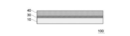
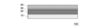
図1および2は、本発明に係る実施形態の粘着性フィルム100の構造の一例を模式的に示した断面図である。
本実施形態に係る半導体装置の製造方法は、以下の3つの工程を少なくとも備えている。
(A)回路形成面を有する半導体ウェハと、上記半導体ウェハの上記回路形成面側に貼り合わされた粘着性フィルム100と、を備える構造体を準備する工程。
(B)上記半導体ウェハの上記回路形成面側とは反対側の面をバックグラインドする工程。
(C)粘着性フィルム100に紫外線を照射した後に上記半導体ウェハから粘着性フィルム100を除去する工程。
そして、粘着性フィルム100として、基材層10と、帯電防止層30と、導電性添加剤を含む粘着性樹脂層40と、をこの順番に備え、粘着性樹脂層40が上記半導体ウェハの上記回路形成面側となるように用いる粘着性フィルムを使用する。
1 and 2 are cross-sectional views schematically showing an example of the structure of an
The method for manufacturing a semiconductor device according to this embodiment includes at least the following three steps.
(A) A step of preparing a structure comprising a semiconductor wafer having a circuit forming surface and an
(B) Backgrinding the surface of the semiconductor wafer opposite to the circuit forming surface.
(C) a step of removing the
The
1.粘着性フィルム
はじめに、本実施形態に係る半導体装置の製造方法で用いる粘着性フィルム100について説明する。
1. Adhesive Film First, the
上述したように、近年、半導体ウェハ加工用粘着性フィルムの静電気対策という観点について要求される技術水準は、ますます高くなっている。特に、高密度の回路を配した半導体ウェハの高密度回路上にはんだバンプや銅ピラーバンプ等のバンプ電極が形成された半導体ウェハを用いる場合は、静電気が原因で半導体ウェハに形成したバンプ電極を含む回路の破壊(ショート)が起きやすくなってきている傾向にあるため、このような要求がより顕著になっている。
このため、帯電防止性により優れた半導体ウェハ加工用粘着性フィルムを実現することが求められていた。
As described above, in recent years, the technical level required from the standpoint of countermeasures against static electricity in adhesive films for processing semiconductor wafers is becoming higher and higher. In particular, when using a semiconductor wafer on which bump electrodes such as solder bumps and copper pillar bumps are formed on the high-density circuit of a semiconductor wafer on which high-density circuits are arranged, static electricity causes the bump electrode formed on the semiconductor wafer to be damaged. Such a demand is becoming more conspicuous due to the tendency of circuit breakage (short circuit) to occur more easily.
Therefore, it has been desired to realize an adhesive film for semiconductor wafer processing which is more excellent in antistatic properties.
ここで、本発明者らの検討によれば、特許文献1に記載されているような、基材フィルムと帯電防止層と粘着剤層とがこの順番に積層された粘着性フィルムにおいて、帯電防止性が十分に満足するものではないことが明らかになった。
より具体的には、特許文献1に記載されているような粘着性フィルムは、紫外線硬化後に粘着剤層の飽和帯電圧が大幅に増加し、帯電防止性が大きく悪化してしまうことが明らかになった。
Here, according to the studies of the present inventors, in an adhesive film in which a base film, an antistatic layer, and an adhesive layer are laminated in this order, as described in Patent Document 1, antistatic It became clear that sex was not fully satisfying.
More specifically, it is clear that the adhesive film described in Patent Document 1 significantly increases the saturation voltage of the adhesive layer after UV curing, and greatly deteriorates the antistatic property. became.
本発明者らは、上記課題を達成するために鋭意検討を重ねた。その結果、粘着性フィルムの層構成を、基材層と、帯電防止層と、導電性添加剤を含む粘着性樹脂層と、をこの順番に備える層構成とすることにより、紫外線硬化後の粘着性フィルムの飽和帯電圧の上昇を抑制できることを初めて見出した。
すなわち、本実施形態に係る粘着性フィルム100は、上記層構成とすることで、紫外線硬化後の帯電防止性に優れ、半導体ウェハから剥離する際に発生する静電気の量を抑制でき、品質に優れた半導体部品を安定的に得ることができる。
The inventors of the present invention have made extensive studies in order to achieve the above object. As a result, by making the layer structure of the adhesive film into a layer structure comprising a substrate layer, an antistatic layer, and an adhesive resin layer containing a conductive additive in this order, the adhesive after UV curing can be obtained. It was found for the first time that an increase in the saturation charge voltage of a flexible film can be suppressed.
That is, the
本実施形態に係る粘着性フィルム100において、下記の方法で測定される、紫外線硬化後の粘着性樹脂層40の飽和帯電圧V1が好ましくは1.0kV以下であり、より好ましくは0.5kV以下である。
(方法)
粘着性樹脂層40に対し、25℃の環境下で高圧水銀ランプを用いて主波長365nmの紫外線を照射強度100mW/cm2で紫外線量1080mJ/cm2照射して粘着性樹脂層40を光硬化させる。次いで、印加電圧10kV、試料と電極との距離20mm、25℃、50%RHの条件下で粘着性樹脂層40の表面に電圧の印加を30秒おこない、JIS L1094に準じて粘着性樹脂層40の表面の飽和帯電圧(V1)を算出する。
In the
(Method)
The
紫外線硬化後の粘着性樹脂層40の飽和帯電圧V1を上記上限値以下とすることにより、半導体ウェハ表面への帯電防止性をより一層良好なものとすることができる。
紫外線硬化後の粘着性樹脂層40の飽和帯電圧V1の下限値は、例えば、0.01kV以上であり、好ましくは0kVである。
By setting the saturation voltage V1 of the
The lower limit of the saturation voltage V1 of the
本実施形態において、例えば、粘着性樹脂層40を構成する各成分の種類や配合割合、粘着性樹脂層40の厚み等を適切に調節することにより、紫外線硬化後の粘着性樹脂層40の飽和帯電圧V1を上記上限値以下に制御することが可能である。
これらの中でも、例えば粘着性樹脂層40中の導電性添加剤の有無や、粘着性樹脂層40の厚み等が、紫外線硬化後の粘着性樹脂層40の飽和帯電圧V1を所望の数値範囲とするための要素として挙げられる。
例えば、粘着性樹脂層40中の導電性添加剤の含有量を増やしたり、粘着性樹脂層40の厚みを薄くしたりすると、飽和帯電圧V1を低下させることができる。
In this embodiment, for example, by appropriately adjusting the type and blending ratio of each component constituting the
Among these, for example, the presence or absence of a conductive additive in the
For example, if the content of the conductive additive in the
本実施形態に係る粘着性フィルム100において、下記の方法で測定される、紫外線硬化後の粘着性樹脂層40の表面の飽和帯電圧をV2としたとき、V1/V2が好ましくは5.0以下であり、より好ましくは3.0以下であり、さらに好ましくは2.5以下である。V1/V2が上記上限値以下であると、半導体ウェハから剥離する際に発生する静電気の量をより安定的に抑制でき、品質に優れた半導体部品をより安定的に得ることができる。
(方法)
粘着性樹脂層40に対し、25℃の環境下で高圧水銀ランプを用いて主波長365nmの紫外線を照射強度100mW/cm2で紫外線量200mJ/cm2照射して粘着性樹脂層40を光硬化させる。次いで、印加電圧10kV、試料と電極との距離20mm、25℃、50%RHの条件下で粘着性樹脂層40の表面に電圧の印加を30秒おこない、JIS L1094に準じて粘着性樹脂層40の表面の飽和帯電圧(V2)を算出する。
In the
(Method)
The
本実施形態に係る粘着性フィルム100において、紫外線硬化後の粘着性樹脂層40の飽和帯電圧V1の半減期が、好ましくは20秒以下であり、より好ましくは10秒以下であり、さらに好ましくは5秒以下であり、特に好ましくは1秒以下である。
ここで、飽和帯電圧V1の半減期とは、飽和帯電圧V1の測定において、粘着性樹脂層40の表面への電圧の印加を終了してから帯電圧の値が半分に低下するまでの時間をいう。
本実施形態に係る粘着性フィルム100は、紫外線硬化後の粘着性樹脂層40の飽和帯電圧V1が上記上限値以下であるため、このような短い半減期を実現でき、帯電防止性に優れた粘着性フィルム100とすることができる。
In the
Here, the half -life of the saturated electrification voltage V1 means the period from when the voltage application to the surface of the
The
本実施形態に係る粘着性フィルム100において、下記の方法で測定される、紫外線硬化後の粘着性樹脂層40の表面のタック力が0.1N/cm2以下であることが好ましく、0.05N/cm2以下であることがより好ましく、0.01N/cm2以下であることがさらに好ましい。
紫外線硬化後の粘着性樹脂層40の表面のタック力が上記上限値以下であることにより、半導体ウェハ表面から粘着性フィルム100を剥離することがより容易になり、半導体ウェハ表面へ粘着性樹脂層40の一部が残ってしまうことや、粘着性フィルム100の剥離により半導体ウェハに不具合が発生してしまうこと等をより一層抑制することができる。
(方法)
粘着性フィルム100の粘着性樹脂層40をポリイミドフィルム(例えば、製品名:カプトン200H、東レ・デュポン社製)に貼合し、25℃の環境下で粘着性フィルム100の基材層10側から高圧水銀ランプを用いて主波長365nmの紫外線を照射強度100mW/cm2で紫外線量1080mJ/cm2照射して粘着性樹脂層40を光硬化させる。次いで、ポリイミドフィルムを粘着性フィルム100から剥離し、測定装置としてプローブタックテスター(例えば、「TESTING MACHINES Inc.社製プローブタックテスター:モデル80-02-01」)を用いて、直径5mmのプローブと粘着性樹脂層40の表面とを10mm/秒の速度で接触させ、0.98N/cm2の接触荷重で10秒間接触させた後、10mm/秒の速度で上記プローブを粘着性樹脂層40の表面から垂直方向に剥離する方法で粘着性樹脂層40の表面のタック力を測定する。
In the
When the tack force of the surface of the
(Method)
The
本実施形態に係る粘着性フィルム100全体の厚さは、機械的特性と取扱い性のバランスから、好ましくは25μm以上1000μm以下であり、より好ましくは50μm以上600μm以下である。
The thickness of the entire
本実施形態に係る粘着性フィルム100は、半導体装置の製造工程において、半導体ウェハの回路形成面を保護するために用いられ、より具体的には半導体装置の製造工程の一つであるバックグラインド工程において半導体ウェハの回路形成面(すなわち回路パターンを含む回路面)を保護するために使用するバックグラインドテープとして用いられる。
ここで、貼り付ける対象の半導体ウェハが表面にバンプ電極を含む微細配線の回路が施された半導体ウェハの場合、半導体ウェハから粘着性フィルムを剥離する際に発生する静電気が原因で半導体ウェハに形成した回路が破壊されるという静電破壊等が起きやすいが、本実施形態に係る粘着性フィルム100を用いることによって、このような表面にバンプ電極が形成された半導体ウェハに対しても静電破壊等をより確実に抑制することが可能となる。
The
Here, if the semiconductor wafer to be pasted is a semiconductor wafer on which fine wiring circuits including bump electrodes are applied to the surface, static electricity generated when the adhesive film is peeled off from the semiconductor wafer causes static electricity to form on the semiconductor wafer. However, by using the
本実施形態に係る粘着性フィルム100を適用できる半導体ウェハとしては特に限定されず、シリコンウェハ等が挙げられる。
A semiconductor wafer to which the
次に、本実施形態に係る粘着性フィルム100を構成する各層について説明する。
Next, each layer constituting the
(基材層)
基材層10は、粘着性フィルム100の取り扱い性や機械的特性、耐熱性等の特性をより良好にすることを目的として設けられる層である。
基材層10は、半導体ウェハを加工する際に加わる外力に耐えうる機械的強度があれば特に限定されないが、例えば、樹脂フィルムが挙げられる。
上記樹脂フィルムを構成する樹脂としては、公知の熱可塑性樹脂を用いることができる。例えば、ポリエチレン、ポリプロピレン、ポリ(4-メチル-1-ペンテン)、ポリ(1-ブテン)等のポリオレフィン;ポリエチレンテレフタレート、ポリブチレンテレフタレート等のポリエステル;ナイロン-6、ナイロン-66、ポリメタキシレンアジパミド等のポリアミド;ポリアクリレート;ポリメタアクリレート;ポリ塩化ビニル;ポリエーテルイミド;エチレン・酢酸ビニル共重合体;ポリアクリロニトリル;ポリカーボネート;ポリスチレン;アイオノマー;ポリスルホン;ポリエーテルスルホン;ポリフェニレンエーテル等から選択される一種または二種以上を挙げることができる。
これらの中でも、半導体ウェハ保護の観点から、ポリプロピレン、ポリエチレンテレフタレート、ポリアミド、エチレン・酢酸ビニル共重合体から選択される一種または二種以上が好ましく、ポリエチレンテレフタレート、エチレン・酢酸ビニル共重合体から選択される一種または二種以上がより好ましい。
(Base material layer)
The
The
A known thermoplastic resin can be used as the resin constituting the resin film. For example, polyolefins such as polyethylene, polypropylene, poly(4-methyl-1-pentene) and poly(1-butene); polyesters such as polyethylene terephthalate and polybutylene terephthalate; nylon-6, nylon-66, polymetaxylene adipate polymethacrylate; polyvinyl chloride; polyetherimide; ethylene-vinyl acetate copolymer; polyacrylonitrile; polycarbonate; 1 type, or 2 or more types can be mentioned.
Among these, from the viewpoint of semiconductor wafer protection, one or more selected from polypropylene, polyethylene terephthalate, polyamide, and ethylene/vinyl acetate copolymer is preferable, and polyethylene terephthalate and ethylene/vinyl acetate copolymer are selected. more preferably one or two or more.
基材層10は、単層であっても、二種以上の層であってもよい。
また、基材層10を形成するために使用する樹脂フィルムの形態としては、延伸フィルムであってもよいし、一軸方向または二軸方向に延伸したフィルムであってもよいが、基材層10の機械的強度を向上させる観点から、一軸方向または二軸方向に延伸したフィルムであることが好ましい。
The
The form of the resin film used to form the
基材層10の厚さは、良好なフィルム特性を得る観点から、好ましくは10μm以上500μm以下、より好ましくは20μm以上300μm以下、さらに好ましくは25μm以上150μm以下である。
基材層10は他の層との接着性を改良するために、表面処理を行ってもよい。具体的には、コロナ処理、プラズマ処理、アンダーコート処理、プライマーコート処理等を行ってもよい。
The thickness of the
The
(粘着性樹脂層)
本実施形態に係る粘着性フィルム100は粘着性樹脂層40を備えている。
粘着性樹脂層40は粘着性フィルム100を半導体ウェハに貼り付ける際に、半導体ウェハの表面に接触して粘着する層である。
(Adhesive resin layer)
The
The
粘着性樹脂層40は、紫外線硬化型粘着性樹脂を含む紫外線硬化型粘着剤により形成された層であることが好ましい。
紫外線硬化型粘着剤としては、例えば、(メタ)アクリル系粘着剤、シリコーン系粘着剤、ウレタン系粘着剤等が挙げられる。
(メタ)アクリル系粘着剤は、紫外線硬化型粘着性樹脂として(メタ)アクリル系粘着性樹脂を必須成分として含んでいる。シリコーン系粘着剤は、紫外線硬化型粘着性樹脂としてシリコーン系粘着性樹脂を必須成分として含んでいる。ウレタン系粘着剤は、紫外線硬化型粘着性樹脂としてウレタン系粘着性樹脂を必須成分として含んでいる。
これらの中でも粘着力の調整を容易にする観点等から、(メタ)アクリル系粘着剤が好ましい。
The
Examples of UV-curable adhesives include (meth)acrylic adhesives, silicone adhesives, urethane adhesives, and the like.
The (meth)acrylic pressure-sensitive adhesive contains a (meth)acrylic pressure-sensitive adhesive resin as an essential component as an ultraviolet curable pressure-sensitive adhesive resin. The silicone-based pressure-sensitive adhesive contains a silicone-based pressure-sensitive adhesive resin as an essential component as an ultraviolet-curable pressure-sensitive adhesive resin. The urethane-based adhesive contains a urethane-based adhesive resin as an essential component as an ultraviolet-curable adhesive resin.
Among these, the (meth)acrylic pressure-sensitive adhesive is preferable from the viewpoint of facilitating the adjustment of the adhesive force.
(メタ)アクリル系粘着剤としては、分子中に重合性炭素-炭素二重結合を有する(メタ)アクリル系粘着性樹脂と、分子内に重合性炭素-炭素二重結合を2個以上有する低分子量化合物と、光開始剤を含み、必要に応じて架橋剤により上記(メタ)アクリル系粘着性樹脂を架橋させて得られる粘着剤を例示することができる。 The (meth)acrylic adhesive includes a (meth)acrylic adhesive resin having a polymerizable carbon-carbon double bond in the molecule and a low polymerizable carbon-carbon double bond having two or more polymerizable carbon-carbon double bonds in the molecule. A pressure-sensitive adhesive obtained by cross-linking the above (meth)acrylic pressure-sensitive adhesive resin with a cross-linking agent, if necessary, may be exemplified.
分子中に重合性炭素-炭素二重結合を有する(メタ)アクリル系粘着性樹脂は、具体的には次のようにして得られる。まず、エチレン性二重結合を有するモノマーと官能基(P)を有する共重合性モノマーを共重合させる。次いで、この共重合体に含まれる官能基(P)と、該官能基(P)と付加反応、縮合反応等を起こしうる官能基(Q)を有するモノマーとを、該モノマー中の二重結合を残したまま反応させ、共重合体分子中に重合性炭素-炭素二重結合を導入する。 A (meth)acrylic adhesive resin having a polymerizable carbon-carbon double bond in the molecule is specifically obtained as follows. First, a monomer having an ethylenic double bond and a copolymerizable monomer having a functional group (P) are copolymerized. Next, a functional group (P) contained in this copolymer and a monomer having a functional group (Q) capable of undergoing an addition reaction, a condensation reaction, or the like with the functional group (P) are combined to form a double bond in the monomer. is left to react to introduce a polymerizable carbon-carbon double bond into the copolymer molecule.
上記エチレン性二重結合を有するモノマーとしては、例えば、(メタ)アクリル酸メチル、(メタ)アクリル酸-2-エチルヘキシル、(メタ)アクリル酸ブチル、(メタ)アクリル酸エチル等のアクリル酸アルキルエステル及びメタクリル酸アルキルエステルモノマー、酢酸ビニルの如きビニルエステル、(メタ)アクリロニトリル、(メタ)アクリルアミド、スチレン等のエチレン性二重結合を有するモノマーの中から、1種又は2種以上が用いられる。 Examples of monomers having an ethylenic double bond include alkyl acrylates such as methyl (meth)acrylate, 2-ethylhexyl (meth)acrylate, butyl (meth)acrylate, and ethyl (meth)acrylate. and methacrylic acid alkyl ester monomers, vinyl esters such as vinyl acetate, (meth)acrylonitrile, (meth)acrylamide, and monomers having an ethylenic double bond such as styrene.
上記官能基(P)を有する共重合性モノマーとしては、(メタ)アクリル酸、マレイン酸、(メタ)アクリル酸2-ヒドロキシエチル、(メタ)アクリル酸グリシジル、Nーメチロール(メタ)アクリルアミド、(メタ)アクリロイルオキシエチルイソシアネート等が挙げられる。これらは1種でもよく、2種以上組み合わせて使用してもよい。上記エチレン性二重結合を有するモノマーと官能基(P)を有する共重合性モノマーの割合は、前者70~99質量%に対し、後者30~1質量%が好ましい。さらに好ましくは、前者80~95質量%に対し、後者20~5質量%である。
上記官能基(Q)を有するモノマーとしては、例えば、上記官能基(P)を有する共重合性モノマーと同様のモノマーを挙げることができる。
Examples of copolymerizable monomers having the functional group (P) include (meth) acrylic acid, maleic acid, 2-hydroxyethyl (meth) acrylate, glycidyl (meth) acrylate, N-methylol (meth) acrylamide, (meth) ) acryloyloxyethyl isocyanate and the like. These may be used alone or in combination of two or more. The ratio of the monomer having an ethylenic double bond and the copolymerizable monomer having a functional group (P) is preferably 70 to 99% by mass for the former and 30 to 1% by mass for the latter. More preferably, the former is 80 to 95% by mass and the latter is 20 to 5% by mass.
Examples of the monomer having the functional group (Q) include monomers similar to the copolymerizable monomer having the functional group (P).
エチレン性二重結合を有するモノマーと官能基(P)を有する共重合性モノマーとの共重合体に、重合性炭素-炭素二重結合を導入する際に反応させる官能基(P)と官能基(Q)の組み合わせとして、カルボキシル基とエポキシ基、カルボキシル基とアジリジル基、水酸基とイソシアネート基等、容易に付加反応が起こる組み合わせが望ましい。又、付加反応に限らずカルボン酸基と水酸基との縮合反応等、重合性炭素-炭素二重結合が容易に導入できる反応であれば如何なる反応を用いてもよい。 A functional group (P) and a functional group to be reacted when introducing a polymerizable carbon-carbon double bond into a copolymer of a monomer having an ethylenic double bond and a copolymerizable monomer having a functional group (P) As the combination of (Q), a combination such as a carboxyl group and an epoxy group, a carboxyl group and an aziridyl group, a hydroxyl group and an isocyanate group, etc., in which an addition reaction easily occurs is desirable. In addition to the addition reaction, any reaction such as a condensation reaction between a carboxylic acid group and a hydroxyl group may be used as long as the reaction can easily introduce a polymerizable carbon-carbon double bond.
分子中に重合性炭素-炭素二重結合を2個以上有する低分子量化合物としては、トリプロピレングリコールジ(メタ)アクリレート、トリメチロールプロパントリ(メタ)アクリレート、テトラメチロールメタンテトラアクリレート、ペンタエリスリトールテトラ(メタ)アクリレート、ジペンタエリスリトールモノヒドロキシペンタ(メタ)アクリレート、ジペンタエリスリトールヘキサ(メタ)アクリレート等が挙げられる。これらは1種又は2種以上を用いてもよい。分子中に重合性炭素-炭素二重結合を2個以上有する低分子量化合物の添加量は、上記(メタ)アクリル系粘着性樹脂100質量部に対して、好ましくは0.1~20質量部であり、より好ましくは5~18質量部である。 Examples of low molecular weight compounds having two or more polymerizable carbon-carbon double bonds in the molecule include tripropylene glycol di(meth)acrylate, trimethylolpropane tri(meth)acrylate, tetramethylolmethane tetraacrylate, pentaerythritol tetra( meth)acrylate, dipentaerythritol monohydroxypenta(meth)acrylate, dipentaerythritol hexa(meth)acrylate and the like. These may use 1 type(s) or 2 or more types. The amount of the low molecular weight compound having two or more polymerizable carbon-carbon double bonds in the molecule is preferably 0.1 to 20 parts by mass with respect to 100 parts by mass of the (meth)acrylic adhesive resin. Yes, more preferably 5 to 18 parts by mass.
光開始剤としては、ベンゾイン、イソプロピルベンゾインエーテル、イソブチルベンゾインエーテル、ベンゾフェノン、ミヒラーケトン、クロロチオキサントン、ドデシルチオキサントン、ジメチルチオキサントン、ジエチルチオキサントン、アセトフェノンジエチルケタール、ベンジルジメチルケタール、1-ヒドロキシシクロヘキシルフェニルケトン、2-ヒドロキシ-2-メチル-1-フェニルプロパン-1-オン等が挙げられる。これらは1種又は2種以上用いてもよい。光開始剤の添加量は、上記(メタ)アクリル系粘着性樹脂100質量部に対して、好ましくは0.1~15質量部であり、より好ましくは5~10質量部である。 Photoinitiators include benzoin, isopropylbenzoin ether, isobutylbenzoin ether, benzophenone, Michler ketone, chlorothioxanthone, dodecylthioxanthone, dimethylthioxanthone, diethylthioxanthone, acetophenone diethyl ketal, benzyl dimethyl ketal, 1-hydroxycyclohexylphenyl ketone, 2-hydroxy -2-methyl-1-phenylpropan-1-one and the like. You may use these 1 type(s) or 2 or more types. The amount of the photoinitiator to be added is preferably 0.1 to 15 parts by mass, more preferably 5 to 10 parts by mass, based on 100 parts by mass of the (meth)acrylic adhesive resin.
上記紫外線硬化型粘着剤には架橋剤を添加してもよい。架橋剤として、ソルビトールポリグリシジルエーテル、ポリグリセロールポリグリシジルエーテル、ペンタエリスリトールポリグリシジルエーテル、ジグリセロールポリグリシジルエーテル等のエポキシ系化合物、テトラメチロールメタン-トリ-β-アジリジニルプロピオネート、トリメチロールプロパン-トリ-β-アジリジニルプロピオネート、N,N'-ジフェニルメタン-4,4'-ビス(1-アジリジンカルボキシアミド)、N,N'-ヘキサメチレン-1,6-ビス(1-アジリジンカルボキシアミド)等のアジリジン系化合物、テトラメチレンジイソシアネート、ヘキサメチレンジイソシアネート、ポリイソシアネート等のイソシアネート系化合物等が挙げられる。上記紫外線硬化型粘着剤は、溶剤タイプ、エマルションタイプ、ホットメルトタイプ等の何れでもよい。 A cross-linking agent may be added to the ultraviolet curable pressure-sensitive adhesive. As a cross-linking agent, epoxy compounds such as sorbitol polyglycidyl ether, polyglycerol polyglycidyl ether, pentaerythritol polyglycidyl ether, diglycerol polyglycidyl ether, tetramethylolmethane-tri-β-aziridinylpropionate, trimethylolpropane -tri-β-aziridinylpropionate, N,N'-diphenylmethane-4,4'-bis(1-aziridinecarboxamide), N,N'-hexamethylene-1,6-bis(1-aziridine aziridine compounds such as carboxamide), and isocyanate compounds such as tetramethylene diisocyanate, hexamethylene diisocyanate and polyisocyanate. The above UV curable pressure sensitive adhesive may be solvent type, emulsion type, hot melt type or the like.
架橋剤の含有量は、通常、架橋剤中の官能基数が(メタ)アクリル系粘着性樹脂中の官能基数よりも多くならない程度の範囲が好ましい。しかし、架橋反応で新たに官能基が生じる場合や、架橋反応が遅い場合等、必要に応じて過剰に含有してもよい。
(メタ)アクリル系粘着剤中の架橋剤の含有量は、粘着性樹脂層40の耐熱性や密着力とのバランスを向上させる観点から、(メタ)アクリル系粘着性樹脂100質量部に対し、0.1質量部以上15質量部以下であることが好ましい。
The content of the cross-linking agent is generally preferably within a range in which the number of functional groups in the cross-linking agent does not exceed the number of functional groups in the (meth)acrylic pressure-sensitive adhesive resin. However, if the cross-linking reaction newly generates a functional group, or if the cross-linking reaction is slow, it may be contained in an excessive amount, if necessary.
From the viewpoint of improving the balance between the heat resistance and adhesion of the
本実施形態に係る粘着性樹脂層40は導電性添加剤を含む。これにより、粘着性樹脂層40の帯電防止性を向上させることができる。さらに、紫外線硬化後の粘着性フィルム100の飽和帯電圧の上昇を抑制することができる。
導電性添加剤としては、例えば、カチオン性界面活性剤、アニオン性界面活性剤、ノニオン性界面活性剤、両性界面活性剤、イオン液体等が挙げられる。粘着性樹脂層40の帯電防止性をより向上できる観点からカチオン性界面活性剤およびアニオン性界面活性剤から選択される少なくとも一種が好ましく、カチオン性界面活性剤がより好ましい。
The
Examples of conductive additives include cationic surfactants, anionic surfactants, nonionic surfactants, amphoteric surfactants, and ionic liquids. From the viewpoint of further improving the antistatic property of the
カチオン性界面活性剤としては、例えば、ドデシルトリメチルアンモニウムクロライド、テトラデシルジメチルベンジルアンモニウムクロライド、セチルジメチルベンジルアンモニウムクロライド、ステアリルジメチルベンジルアンモニウムクロライド、テトラデシルトリメチルアンモニウムクロライド、ヘキサデシルトリメチルアンモニウムクロライド、オクタデシルトリメチルアンモニウムクロライド、ジドデシルジメチルアンモニウムクロライド、ジテトラデシルジメチルアンモニウムクロライド、ジヘキサデシルジメチルアンモニウムクロライド、ジオクタデシルジメチルアンモニウムクロライド、ドデシルベンジルジメチルアンモニウムクロライド、ヘキサデシルベンジルジメチルアンモニウムクロライド、オクタデシルベンジルジメチルアンモニウムクロライド、パルミチルトリメチルアンモニウムクロライド、オレイルトリメチルアンモニウムクロライド、ジバルミチルベンジルメチルアンモニウムクロライド、ジオレイルベンジルメチルアンモニウムクロライド等が挙げられる。
カチオン性界面活性剤としては第4級アンモニウム塩またはアミン塩型を挙げることができ、第4級アンモニウム塩が好ましい。
中でも、テトラデシルジメチルベンジルアンモニウムクロライド、セチルジメチルベンジルアンモニウムクロライド、およびステアリルジメチルベンジルアンモニウムクロライドから選択される少なくとも一種が好ましい。これらの中でも、テトラデシルジメチルベンジルアンモニウムクロライドが特に好ましい。
Examples of cationic surfactants include dodecyltrimethylammonium chloride, tetradecyldimethylbenzylammonium chloride, cetyldimethylbenzylammonium chloride, stearyldimethylbenzylammonium chloride, tetradecyltrimethylammonium chloride, hexadecyltrimethylammonium chloride, and octadecyltrimethylammonium chloride. , didodecyldimethylammonium chloride, ditetradecyldimethylammonium chloride, dihexadecyldimethylammonium chloride, dioctadecyldimethylammonium chloride, dodecylbenzyldimethylammonium chloride, hexadecylbenzyldimethylammonium chloride, octadecylbenzyldimethylammonium chloride, palmityltrimethylammonium chloride chloride, oleyltrimethylammonium chloride, divalmitylbenzylmethylammonium chloride, dioleylbenzylmethylammonium chloride and the like.
Cationic surfactants include quaternary ammonium salts or amine salt types, with quaternary ammonium salts being preferred.
Among them, at least one selected from tetradecyldimethylbenzylammonium chloride, cetyldimethylbenzylammonium chloride, and stearyldimethylbenzylammonium chloride is preferable. Among these, tetradecyldimethylbenzylammonium chloride is particularly preferred.
アニオン性界面活性剤としては、例えば、ドデシルジフェニルエーテルジスルホン酸ジアンモニウム、ドデシルジフェニルエーテルジスルホン酸ナトリウム、ドデシルジフェニルエーテルジスルホン酸カルシウム、アルキルジフェニルエーテルジスルホン酸ナトリウム等のアルキルジフェニルエーテルジスルホン酸塩;ドデシルベンゼンスルホン酸ナトリウム、ドデシルベンゼンスルホン酸アンモニウム等のアルキルベンゼンスルホン酸塩;ラウリル硫酸ナトリウム、ラウリル硫酸アンモニウム等のアルキル硫酸エステル塩;脂肪酸ナトリウム、オレイン酸カリウム等の脂肪族カルボン酸塩;ポリオキシアルキレン単位含有硫酸エステル塩(例えば、ポリオキシエチレンアルキルエーテル硫酸ナトリウム、ポリオキシエチレンアルキルエーテル硫酸アンモニウム等のポリオキシエチレンアルキルエーテル硫酸エステル塩;ポリオキシエチレンアルキルフェニルエーテル硫酸ナトリウム、ポリオキシエチレンアルキルフェニルエーテル硫酸アンモニウム等のポリオキシエチレンアルキルフェニルエーテル硫酸エステル塩;ポリオキシエチレン多環フェニルエーテル硫酸ナトリウム、ポリオキシエチレン多環フェニルエーテル硫酸アンモニウム等のポリオキシエチレン多環フェニルエーテル硫酸エステル塩等);ナフタレンスルホン酸ホルマリン縮合物ナトリウム等のナフタレンスルホン酸ホルマリン縮合物塩;ジアルキルスルホコハク酸ナトリウム、モノアルキルスルホコハク酸ジナトリウム等のアルキルスルホコハク酸塩;ポリオキシエチレン-ポリオキシプロピレングリコールエーテル硫酸塩;スルホン酸塩または硫酸エステル基と重合性の炭素-炭素(不飽和)二重結合とを分子中に有する界面活性剤等が挙げられる。 Examples of anionic surfactants include alkyl diphenyl ether disulfonates such as diammonium dodecyl diphenyl ether disulfonate, sodium dodecyl diphenyl ether disulfonate, calcium dodecyl diphenyl ether disulfonate, sodium alkyl diphenyl ether disulfonate; sodium dodecyl benzene sulfonate, dodecyl benzene Alkylbenzenesulfonates such as ammonium sulfonate; Alkyl sulfate ester salts such as sodium lauryl sulfate and ammonium lauryl sulfate; Aliphatic carboxylate salts such as fatty acid sodium and potassium oleate; Polyoxyethylene alkyl ether sulfate salts such as sodium ethylene alkyl ether sulfate and ammonium polyoxyethylene alkyl ether sulfate; polyoxyethylene alkyl phenyl ether sulfate salts such as sodium polyoxyethylene alkyl phenyl ether sulfate and ammonium polyoxyethylene alkyl phenyl ether sulfate polyoxyethylene polycyclic phenyl ether sulfate salts such as sodium polyoxyethylene polycyclic phenyl ether sulfate and ammonium polyoxyethylene polycyclic phenyl ether sulfate); naphthalene sulfonic acid formalin condensate salts such as sodium naphthalene sulfonic acid formalin condensate alkyl sulfosuccinates such as sodium dialkyl sulfosuccinate and disodium monoalkyl sulfosuccinate; polyoxyethylene-polyoxypropylene glycol ether sulfate; Examples thereof include surfactants having a heavy bond in the molecule.
ノニオン性界面活性剤としては、例えば、ポリオキシエチレンラウリルエーテル、ポリオキシエチレンステアリルエーテル、ポリオキシエチレントリデシルエーテル、ポリオキシエチレンオレイルエーテル等のポリオキシアルキレンアルキルエーテル化合物、ポリオキシエチレンオクチルフェニルエーテル、ポリオキシエチレンノニルフェニルエーテル等のポリオキシアルキレンアルキルフェニルエーテル化合物、ポリオキシエチレン多環フェニルエーテル等のポリオキシアルキレン多環フェニルエーテル化合物等のポリオキシアルキレン単位含有エーテル化合物;ポリオキシエチレンモノラウレート、ポリオキシエチレンモノステアレート、ポリオキシエチレンモノオレエート等のポリオキシアルキレンアルキルエステル化合物;ポリオキシエチレンアルキルアミン等のポリオキシアルキレンアルキルアミン化合物;ソルビタンモノラウレート、ソルビタンモノステアレート、ソルビタントリオレート、ポリオキシエチレンソルビタンモノラウレート、ポリオキシエチレンソルビタンモノオレート等のソルビタン化合物等が挙げられる。 Examples of nonionic surfactants include polyoxyalkylene alkyl ether compounds such as polyoxyethylene lauryl ether, polyoxyethylene stearyl ether, polyoxyethylene tridecyl ether, and polyoxyethylene oleyl ether, polyoxyethylene octylphenyl ether, Polyoxyalkylene alkylphenyl ether compounds such as polyoxyethylene nonylphenyl ether, polyoxyalkylene unit-containing ether compounds such as polyoxyalkylene polycyclic phenyl ether compounds such as polyoxyethylene polycyclic phenyl ether; polyoxyethylene monolaurate, polyoxyalkylene alkyl ester compounds such as polyoxyethylene monostearate and polyoxyethylene monooleate; polyoxyalkylene alkylamine compounds such as polyoxyethylene alkylamine; sorbitan monolaurate, sorbitan monostearate, sorbitan trioleate, Sorbitan compounds such as polyoxyethylene sorbitan monolaurate, polyoxyethylene sorbitan monooleate, and the like.
両性界面活性剤としては、ラウリルベタイン、ラウリルジメチルアミンオキサイド等が挙げられる。 Amphoteric surfactants include lauryl betaine, lauryldimethylamine oxide and the like.
これらの導電性添加剤は1種単独で使用してもよいし、2種以上を組み合わせて使用してもよい。
粘着性樹脂層40中の導電性添加剤の含有量は、紫外線硬化型粘着性樹脂100質量部に対し、0.01質量部以上10質量部以下であることが好ましく、0.1質量部以上5質量部以下であることがより好ましく、0.1質量部以上2質量部以下であることがさらに好ましい。
These conductive additives may be used singly or in combination of two or more.
The content of the conductive additive in the
粘着性樹脂層40は、例えば、帯電防止層30上に粘着剤塗布液を塗布することにより形成することができる。
粘着剤塗布液を塗布する方法としては、従来公知の塗布方法、例えば、ロールコーター法、リバースロールコーター法、グラビアロール法、バーコート法、コンマコーター法、ダイコーター法等が採用できる。塗布された粘着剤の乾燥条件には特に制限はないが、一般的には、80~200℃の温度範囲において、10秒~10分間乾燥することが好ましい。更に好ましくは、80~170℃において、15秒~5分間乾燥する。架橋剤と(メタ)アクリル系粘着性樹脂との架橋反応を十分に促進させるために、粘着剤塗布液の乾燥が終了した後、40~80℃において5~300時間程度加熱してもよい。
The
As a method for applying the adhesive coating liquid, conventionally known coating methods such as roll coater method, reverse roll coater method, gravure roll method, bar coater method, comma coater method and die coater method can be employed. Although there are no particular restrictions on the drying conditions for the applied pressure-sensitive adhesive, it is generally preferred to dry in a temperature range of 80 to 200° C. for 10 seconds to 10 minutes. More preferably, it is dried at 80 to 170°C for 15 seconds to 5 minutes. In order to sufficiently accelerate the cross-linking reaction between the cross-linking agent and the (meth)acrylic adhesive resin, the pressure-sensitive adhesive coating liquid may be heated at 40 to 80° C. for about 5 to 300 hours after drying.
本実施形態に係る粘着性フィルム100において、粘着性樹脂層40の厚みは通常5μm以上550μm以下であり、好ましくは10μm以上400μm以下であり、さらに好ましくは30μm以上300μm以下、特に好ましくは50μm以上250μm以下である。粘着性樹脂層40の厚みが上記範囲内であると、半導体ウェハ表面への粘着性と、取扱い性とのバランスが良好である。
また、本実施形態に係る粘着性フィルム100が後述の凹凸吸収性樹脂層20をさらに備える場合、粘着性樹脂層40の厚みは100μm以下が好ましく、50μm以下がより好ましく、30μm未満であることがさらに好ましく、25μm以下であることがよりさらに好ましく、20μm未満であることがよりさらに好ましく、15μm以下であることが特に好ましい。これにより、粘着性樹脂層40の表面と帯電防止層30との距離を小さくすることができ、その結果、粘着性フィルム100の帯電防止性をより良好にすることができる。また、本実施形態に係る粘着性フィルム100が後述の凹凸吸収性樹脂層20をさらに備える場合、粘着性樹脂層40の厚みの下限値は特に限定されないが、粘着力を良好にする観点から、0.5μm以上が好ましく、1.0μm以上がより好ましく、3.0μm以上がさらに好ましく、5.0μm以上が特に好ましい。
In the
Further, when the
(帯電防止層)
本実施形態に係る粘着性フィルム100は帯電防止層30を備えている。これにより、粘着性フィルム100の粘着性を維持したまま、粘着性フィルム100の帯電防止性を向上でき、半導体ウェハから粘着性フィルム100を剥離する際に発生する静電気の量を抑制することができる。
(Antistatic layer)
The
帯電防止層30を構成する材料は、帯電防止層30の表面抵抗値を低下させて剥離に伴う静電気の発生を抑制する観点から、導電性高分子を含むことが好ましい。
導電性高分子としては、例えば、ポリチオフェン系導電性高分子、ポリピロール系導電性高分子、ポリアニリン系導電性高分子、ポリ(p-フェニレンビニレン)系導電性高分子、ポリキノキサリン系導電性高分子等が挙げられる。
光学特性や外観、帯電防止性、塗工性、安定性等のバランスが良好であるという観点からポリチオフェン系導電性高分子が好ましい。ポリチオフェン系導電性高分子としては、例えば、ポリエチレンジオキシチオフェン、ポリチオフェンが挙げられる。
これらの導電性高分子は1種単独で使用してもよいし、2種以上を組み合わせて使用してもよい。
The material constituting the
Examples of conductive polymers include polythiophene-based conductive polymers, polypyrrole-based conductive polymers, polyaniline-based conductive polymers, poly(p-phenylene vinylene)-based conductive polymers, and polyquinoxaline-based conductive polymers. etc.
A polythiophene-based conductive polymer is preferable from the viewpoint of a good balance among optical properties, appearance, antistatic properties, coatability, stability, and the like. Examples of polythiophene-based conductive polymers include polyethylenedioxythiophene and polythiophene.
These conductive polymers may be used singly or in combination of two or more.
帯電防止層30を形成する材料は、例えば、ドーピング剤、バインダー樹脂等をさらに含むことができる。
ドーピング剤は、ドーパントとして機能して、導電性高分子に導電性をより確実に付与(ドーピング)するものであって、例えば、スルホン酸系化合物が挙げられる。
The material forming the
The doping agent functions as a dopant to more reliably impart (dope) conductivity to the conductive polymer, and examples thereof include sulfonic acid compounds.
スルホン酸系化合物は、例えば、p-トルエンスルホン酸、ベンゼンスルホン酸、エチルベンゼンスルホン酸、オクチルベンゼンスルホン酸、ドデシルベンゼンスルホン酸、メシチレンスルホン酸、m-キシレンスルホン酸、ポリスチレンスルホン酸、ポリビニルスルホン酸等が挙げられる。導電性高分子の溶解性や水分散性を向上させる観点から、ポリスチレンスルホン酸やポリビニルスルホン酸が好ましい。
スルホン酸系化合物は1種単独で使用してもよいし、2種以上を組み合わせて使用してもよい。
Sulfonic acid compounds include, for example, p-toluenesulfonic acid, benzenesulfonic acid, ethylbenzenesulfonic acid, octylbenzenesulfonic acid, dodecylbenzenesulfonic acid, mesitylenesulfonic acid, m-xylenesulfonic acid, polystyrenesulfonic acid, polyvinylsulfonic acid, and the like. is mentioned. Polystyrene sulfonic acid and polyvinyl sulfonic acid are preferred from the viewpoint of improving the solubility and water dispersibility of the conductive polymer.
The sulfonic acid compounds may be used singly or in combination of two or more.
このようドーピング剤を添加することにより、導電性高分子とスルホン酸系化合物とが一部反応してスルホン酸塩を形成し、このスルホン酸塩の作用により帯電防止層30の帯電防止機能がより一層向上する。
ドーピング剤の配合割合は、導電性高分子100質量部に対して、例えば、100~300質量部である。
導電性高分子とドーピング剤との組み合わせとしては、ポリエチレンジオキシチオフェン(PEDOT)とポリスチレンスルホン酸(PSS)との組み合わせが帯電防止性により優れるため好ましい。
By adding such a doping agent, the conductive polymer and the sulfonic acid compound partially react to form a sulfonate, and the action of this sulfonate enhances the antistatic function of the
The mixing ratio of the doping agent is, for example, 100 to 300 parts by mass with respect to 100 parts by mass of the conductive polymer.
As a combination of a conductive polymer and a doping agent, a combination of polyethylenedioxythiophene (PEDOT) and polystyrene sulfonic acid (PSS) is preferable because of its excellent antistatic properties.
帯電防止層30を構成する材料は、皮膜形成性や密着性等を向上させる観点から、バインダー樹脂をさらに含んでもよい。
バインダー樹脂としては、例えば、ポリウレタン系樹脂、ポリエステル系樹脂、(メタ)アクリル系樹脂、ポリエーテル系樹脂、セルロース系樹脂、ポリビニルアルコール系樹脂、エポキシ樹脂、ポリビニルピロリドン、ポリスチレン系樹脂、ポリエチレングリコール、ペンタエリスリトール等が挙げられる。
バインダー樹脂は1種単独で使用してもよいし、2種以上を組み合わせて使用してもよい。バインダー樹脂の含有量は、例えば、導電性高分子100質量部に対して10~500質量部である。
The material forming the
Examples of binder resins include polyurethane-based resins, polyester-based resins, (meth)acrylic-based resins, polyether-based resins, cellulose-based resins, polyvinyl alcohol-based resins, epoxy resins, polyvinylpyrrolidone, polystyrene-based resins, polyethylene glycol, penta erythritol and the like.
Binder resin may be used individually by 1 type, and may be used in combination of 2 or more type. The content of the binder resin is, for example, 10 to 500 parts by mass with respect to 100 parts by mass of the conductive polymer.
帯電防止層30の厚みは、帯電防止性能の観点から、0.01μm以上10μm以下であることが好ましく、0.01μm以上5μm以下であることがより好ましく、0.01μm以上1μm以下であることがさらに好ましい。
From the viewpoint of antistatic performance, the thickness of the
(凹凸吸収性樹脂層)
図2に示すように、本実施形態に係る粘着性フィルム100は、基材層10と帯電防止層30との間に凹凸吸収性樹脂層20をさらに備えることが好ましい。
これにより、粘着性フィルム100の凹凸吸収性を良好にしつつ粘着性樹脂層40の厚みを薄くすることが可能となり、粘着性樹脂層40の表面と帯電防止層30との距離を小さくすることができ、その結果、粘着性フィルム100の帯電防止性をより良好にすることができる。
(Uneven absorbent resin layer)
As shown in FIG. 2 , the
This makes it possible to reduce the thickness of the
凹凸吸収性樹脂層20の密度は、機械的強度と凹凸追従性とのバランスの観点から、800~990kg/m3が好ましく、830~980kg/m3がより好ましく、850~970kg/m3がさらに好ましい。
The density of the uneven
凹凸吸収性樹脂層20を構成する樹脂は、凹凸吸収性を示すものであれば特に限定されないが、例えば、熱可塑性樹脂を用いることができる。
より具体的には、オレフィン系樹脂、エチレン・極性モノマー共重合体、ABS樹脂、塩化ビニル樹脂、塩化ビニリデン樹脂、(メタ)アクリル系樹脂、ポリアミド系樹脂、フッ素系樹脂、ポリカーボネート系樹脂、ポリエステル系樹脂等が挙げられる。
これらの中でも、オレフィン系樹脂およびエチレン・極性モノマー共重合体から選択される少なくとも一種が好ましい。
The resin constituting the unevenness-absorbing
More specifically, olefin-based resins, ethylene/polar monomer copolymers, ABS resins, vinyl chloride resins, vinylidene chloride resins, (meth)acrylic resins, polyamide-based resins, fluorine-based resins, polycarbonate-based resins, polyester-based resins Resin etc. are mentioned.
Among these, at least one selected from olefin resins and ethylene/polar monomer copolymers is preferable.
オレフィン系樹脂としては、例えば、直鎖状低密度ポリエチレン(LLDPE)、低密度ポリエチレン、高密度ポリエチレン、ポリプロピレン、エチレンおよび炭素数3~12のα-オレフィンとを含むエチレン・α-オレフィン共重合体、プロピレンおよび炭素数4~12のα-オレフィンとを含むプロピレン・α-オレフィン共重合体、エチレン・環状オレフィン共重合体、エチレン・α-オレフィン・環状オレフィン共重合体等が挙げられる。
エチレン・極性モノマー共重合体としては、エチレン・(メタ)アクリル酸エチル共重合体、エチレン・(メタ)アクリル酸メチル共重合体、エチレン・(メタ)アクリル酸プロピル共重合体、エチレン・(メタ)アクリル酸ブチル共重合体等のエチレン・不飽和カルボン酸エステル共重合体;エチレン・酢酸ビニル共重合体、エチレン・プロピオン酸ビニル共重合体、エチレン・酪酸ビニル共重合体、エチレン・ステアリン酸ビニル共重合体等のエチレン・ビニルエステル共重合体等が挙げられる。
凹凸吸収性樹脂層20を構成する樹脂は単独で用いてもよいし、二種以上をブレンドして用いてもよい。
Examples of olefin-based resins include linear low-density polyethylene (LLDPE), low-density polyethylene, high-density polyethylene, polypropylene, ethylene, and ethylene/α-olefin copolymers containing α-olefins having 3 to 12 carbon atoms. , a propylene/α-olefin copolymer containing propylene and an α-olefin having 4 to 12 carbon atoms, an ethylene/cyclic olefin copolymer, an ethylene/α-olefin/cyclic olefin copolymer, and the like.
Examples of ethylene/polar monomer copolymers include ethylene/ethyl (meth)acrylate copolymer, ethylene/methyl (meth)acrylate copolymer, ethylene/propyl (meth)acrylate copolymer, and ethylene/(meth)acrylate copolymer. ) Ethylene/unsaturated carboxylic acid ester copolymer such as butyl acrylate copolymer; ethylene/vinyl acetate copolymer, ethylene/vinyl propionate copolymer, ethylene/vinyl butyrate copolymer, ethylene/vinyl stearate Examples thereof include ethylene-vinyl ester copolymers such as copolymers.
The resins constituting the uneven absorbing
エチレン・α-オレフィン共重合体における炭素原子数3~12のα-オレフィンは、例えば、プロピレン、1-ブテン、1-ペンテン、3-メチル-1-ブテン、1-ヘキセン、4-メチル-1-ペンテン、3-メチル-1-ペンテン、1-ヘプテン、1-オクテン、1-デセン、1-ドデセン等が挙げられ、好ましくはプロピレン、1-ブテン等である。 The α-olefins having 3 to 12 carbon atoms in the ethylene/α-olefin copolymer are, for example, propylene, 1-butene, 1-pentene, 3-methyl-1-butene, 1-hexene, 4-methyl-1 -pentene, 3-methyl-1-pentene, 1-heptene, 1-octene, 1-decene, 1-dodecene and the like, preferably propylene, 1-butene and the like.
これらの中でも、貼り付け時の凹凸追従性に優れる点で、低密度ポリエチレン;ポリプロピレン;エチレン・プロピレン共重合体、エチレン・1-ブテン共重合体、エチレン・プロピレン・炭素原子数4~12のα-オレフィンの三元共重合体等のエチレン・α-オレフィン共重合体;プロピレン・1-ブテン・炭素原子数5~12のα-オレフィンの三元共重合体;エチレン・酢酸ビニル共重合体等から選択される少なくとも一種が好ましく、エチレン・プロピレン共重合体およびエチレン・酢酸ビニル共重合体から選択される少なくとも一種がより好ましい。 Among these, low-density polyethylene; polypropylene; ethylene-propylene copolymer, ethylene-1-butene copolymer, ethylene-propylene-α having 4 to 12 carbon atoms are preferred in that they are excellent in conformability to irregularities during application. - ethylene/α-olefin copolymers such as olefin terpolymers; propylene/1-butene/α-olefin terpolymers having 5 to 12 carbon atoms; ethylene/vinyl acetate copolymers, etc. At least one selected from is preferable, and at least one selected from ethylene/propylene copolymers and ethylene/vinyl acetate copolymers is more preferable.
凹凸吸収性樹脂層20の厚みは、半導体ウェハの凹凸形成面の凹凸を埋め込むことができる厚みであれば、特に制限されないが、例えば、10μm以上500μm以下であることが好ましく、20μm以上400μm以下であることがより好ましく、30μm以上300μm以下であることがさらに好ましく、50μm以上250μm以下であることが特に好ましい。
The thickness of the irregularity absorbing
本実施形態に係る粘着性フィルム100は、各層の間に接着層(図示せず)を設けていてもよい。この接着層によれば、各層の間の接着性を向上させることができる。
また、本実施形態に係る粘着性フィルム100は、離型フィルムをさらに積層させてもよい。
The
Moreover, the
次に、本実施形態に係る粘着性フィルム100の製造方法の一例を説明する。
Next, an example of a method for manufacturing the
まず、基材層10の一方の面に凹凸吸収性樹脂層20を押出しラミネート法によって形成する。次いで、別途用意した離型フィルム上に所定の導電性材料を塗布し乾燥させることによって、帯電防止層30を形成し、この帯電防止層30を凹凸吸収性樹脂層20上に積層する。次いで、帯電防止層30上に粘着剤塗布液を塗布し乾燥させることによって、粘着性樹脂層40を形成し、粘着性フィルム100が得られる。
また、基材層10と凹凸吸収性樹脂層20とは共押出成形によって形成してもよいし、フィルム状の基材層10とフィルム状の凹凸吸収性樹脂層20とをラミネート(積層)して形成してもよい。
First, the uneven
Further, the
2.半導体装置の製造方法
次に、本実施形態に係る半導体装置の製造方法の各工程について説明する。
2. Method for Manufacturing Semiconductor Device Next, each step of the method for manufacturing a semiconductor device according to this embodiment will be described.
(工程(A))
はじめに、回路形成面を有する半導体ウェハと、半導体ウェハの回路形成面側に貼り合わされた粘着性フィルム100と、を備える構造体を準備する。
このような構造体は、例えば、粘着性フィルム100の粘着性樹脂層40から離型フィルムを剥離し、粘着性樹脂層40の表面を露出させ、その粘着性樹脂層40上に、半導体ウェハの回路形成面を貼り付けることにより作製することができる。
(Step (A))
First, a structure including a semiconductor wafer having a circuit formation surface and an
Such a structure can be obtained, for example, by peeling a release film from the
ここで、粘着性フィルム100に半導体ウェハの回路形成面を貼り付ける際の条件は特に限定されないが、例えば、温度は30~80℃、圧力は0.05~0.5MPaとすることができる。
Here, the conditions for attaching the circuit forming surface of the semiconductor wafer to the
工程(A)は、半導体ウェハの回路形成面に粘着性フィルム100を加温して貼り付けることにより構造体を作製する工程(A2)をさらに含むことが好ましい。これにより、粘着性樹脂層40と半導体ウェハとの接着状態を長時間にわたって良好にすることができる。加温温度としては特に限定されないが、例えば、60~80℃である。
The step (A) preferably further includes a step (A2) of fabricating a structure by heating and attaching the
粘着性フィルム100を半導体ウェハに貼着する操作は、人手により行われる場合もあるが、一般に、ロール状の粘着フィルムを取り付けた自動貼り機と称される装置によって行うことができる。
The operation of attaching the
回路形成面を有する半導体ウェハとしては特に限定されないが、例えば、表面に配線、キャパシタ、ダイオードまたはトランジスタ等の回路が形成されたシリコンウェハ、シリコンカーバイドウェハ、化合物半導体ウェハ、サファイアウェハ等が挙げられる。 The semiconductor wafer having a circuit-forming surface is not particularly limited, but examples thereof include silicon wafers, silicon carbide wafers, compound semiconductor wafers, sapphire wafers, etc. on which circuits such as wiring, capacitors, diodes or transistors are formed.
(工程(B))
次に、上記半導体ウェハの上記回路形成面側とは反対側の面(以下、裏面とも呼ぶ。)をバックグラインドする。
ここで、バックグラインドするとは、半導体ウェハを割ったり、破損したりすることなく、所定の厚みまで薄化加工することを意味する。
例えば、研削機のチャックテーブル等に上記構造体を固定し、半導体ウェハの裏面(回路非形成面)を研削する。
(Step (B))
Next, the surface of the semiconductor wafer opposite to the circuit forming surface (hereinafter also referred to as the back surface) is back ground.
Here, back grinding means thinning the semiconductor wafer to a predetermined thickness without breaking or damaging the wafer.
For example, the structure is fixed to a chuck table or the like of a grinding machine, and the back surface (non-circuit forming surface) of the semiconductor wafer is ground.
このような裏面研削操作において、半導体ウェハは、研削前の厚みが、通常500~1000μmであるのに対して、半導体チップの種類等に応じ、通常100~600μm程度まで研削される。必要に応じて、100μmより薄く削ることもある。研削する前の半導体ウェハの厚みは、半導体ウェハの直径、種類等により適宜決められ、研削後のウェハの厚みは、得られるチップのサイズ、回路の種類等により適宜決められる。 In such a backside grinding operation, the thickness of the semiconductor wafer before grinding is usually 500 to 1000 μm. If necessary, it may be shaved to a thickness of less than 100 μm. The thickness of the semiconductor wafer before grinding is appropriately determined according to the diameter and type of the semiconductor wafer, and the thickness of the wafer after grinding is determined appropriately according to the size of the chip to be obtained, the type of circuit, and the like.
裏面研削方式としては、スルーフィード方式、インフィード方式等の公知の研削方式が採用される。それぞれ研削は、水を半導体ウェハと砥石にかけて冷却しながら行われる。
裏面研削終了後、必要に応じてケミカルエッチングが行われる。ケミカルエッチングは、弗化水素酸、硝酸、硫酸、酢酸等の単独若しくは混合液からなる酸性水溶液、水酸化カリウム水溶液、水酸化ナトリウム水溶液等のアルカリ性水溶液からなる群から選ばれたエッチング液に、粘着性フィルム100を貼着した状態で半導体ウェハを浸漬する等の方法により行われる。該エッチングは、半導体ウェハ裏面に生じた歪みの除去、ウェハのさらなる薄層化、酸化膜等の除去、電極を裏面に形成する際の前処理等を目的として行われる。エッチング液は、上記の目的に応じて適宜選択される。
As the back surface grinding method, a known grinding method such as a through-feed method or an in-feed method is employed. Grinding is performed while cooling the semiconductor wafer and the grinding wheel with water.
After finishing the back surface grinding, chemical etching is performed as necessary. Chemical etching is performed by using an etchant selected from the group consisting of an acidic aqueous solution consisting of hydrofluoric acid, nitric acid, sulfuric acid, acetic acid, etc. alone or a mixed solution, an alkaline aqueous solution such as a potassium hydroxide aqueous solution, a sodium hydroxide aqueous solution, etc. It is carried out by a method such as immersing the semiconductor wafer with the
(工程(C))
次いで、粘着性フィルム100に紫外線を照射した後に上記半導体ウェハから粘着性フィルム100を除去する。
粘着性フィルム100に紫外線を照射することによって、粘着性樹脂層40が光硬化して粘着性樹脂層40の粘着力が低下する。これにより、半導体ウェハから粘着性フィルム100を剥離することができる。
紫外線は、例えば、粘着性フィルム100の基材層10側から照射される。
(Step (C))
Next, after irradiating the
By irradiating the
Ultraviolet rays are irradiated from the
粘着性フィルム100に対して照射する紫外線の線量は、300mJ/cm2以上が好ましく、350mJ/cm2以上がより好ましく、500mJ/cm2以上がさらに好ましい。
紫外線の線量が上記下限値以上であると、粘着性樹脂層40の粘着力を十分に低下させることができ、その結果、半導体ウェハの回路形成面に糊残りが発生することをより抑制することができる。
また、粘着性フィルム100に対して照射する紫外線の線量の上限は特に限定されないが、生産性の観点から、例えば、1500mJ/cm2以下であり、好ましくは1200mJ/cm2以下である。
The dose of ultraviolet rays with which the
When the dose of ultraviolet rays is equal to or higher than the above lower limit, the adhesive strength of the
The upper limit of the dose of ultraviolet rays irradiated to the
粘着性フィルム100に紫外線を照射し、粘着性樹脂層40の粘着力を低下させた後に、粘着性フィルム100を半導体ウェハから剥離する。
半導体ウェハの裏面の研削が完了した後、粘着性フィルム100を剥離する前にケミカルエッチング工程を経ることもある。また、必要に応じて粘着性フィルム100の剥離後に、半導体ウェハ表面に対して、水洗、プラズマ洗浄等の処理が施される。
After the
After the back surface of the semiconductor wafer has been completely ground, a chemical etching process may be performed before the
粘着性フィルム100の剥離は手により行われる場合もあるが、一般には自動剥がし機と称される装置によって行うことができる。
Peeling of the
粘着性フィルム100を剥離した後の半導体ウェハ表面は、必要に応じて洗浄される。洗浄方法としては、水洗浄、溶剤洗浄等の湿式洗浄、プラズマ洗浄等の乾式洗浄等が挙げられる。湿式洗浄の場合、超音波洗浄を併用してもよい。これらの洗浄方法は、半導体ウェハ表面の汚染状況により適宜選択される。
The surface of the semiconductor wafer after peeling off the
(その他の工程)
工程(A)~工程(C)を行った後、半導体ウェハをダイシングして個片化し、半導体チップを得る工程や、得られた半導体チップを回路基板に実装する工程等をさらに行ってもよい。これらの工程は、公知の情報に基づいておこなうことができる。
(Other processes)
After performing steps (A) to (C), a step of dicing the semiconductor wafer into individual pieces to obtain semiconductor chips, a step of mounting the obtained semiconductor chips on a circuit board, and the like may be further performed. . These steps can be performed based on publicly known information.
以上、本発明の実施形態について述べたが、これらは本発明の例示であり、上記以外の様々な構成を採用することもできる。 Although the embodiments of the present invention have been described above, these are examples of the present invention, and various configurations other than those described above can also be adopted.
以下、実施例および比較例により本発明を具体的に説明するが本発明はこれに限定されるものではない。 EXAMPLES The present invention will be specifically described below with reference to Examples and Comparative Examples, but the present invention is not limited thereto.
粘着性フィルムの作製に用いた材料の詳細は以下の通りである。 The details of the materials used to make the adhesive film are as follows.
<基材層>
ポリエチレンテレフタレートフィルム(厚さ50μm)
<Base material layer>
Polyethylene terephthalate film (thickness 50 μm)
<凹凸吸収性樹脂層形成用の樹脂>
凹凸吸収性樹脂1:エチレン・酢酸ビニル共重合体(密度:960kg/m3、三井デュポンポリケミカル社製「エバフレックスEV150」)
<Resin for forming uneven absorbent resin layer>
Concavo-convex absorbent resin 1: Ethylene-vinyl acetate copolymer (density: 960 kg/m 3 , “Evaflex EV150” manufactured by Mitsui DuPont Polychemicals)
<帯電防止層形成用の材料>
帯電防止層形成用材料1:ポリエチレンジオキシチオフェン/ポリスチレンスルホン酸(PEDOT/PSS)を含む導電性材料(ナガセケムテックス社製、商品名:デナトロンP-504CT)
<Material for forming antistatic layer>
Antistatic layer-forming material 1: Conductive material containing polyethylenedioxythiophene/polystyrenesulfonic acid (PEDOT/PSS) (manufactured by Nagase ChemteX Corporation, trade name: Denatron P-504CT)
<導電性添加剤>
導電性添加剤1:テトラデシルジメチルベンジルアンモニウムクロライド(日油社製、商品名:ニッサンカチオンM2-100)
<Conductive additive>
Conductive additive 1: Tetradecyldimethylbenzylammonium chloride (manufactured by NOF Corporation, trade name: Nissan Cation M 2-100 )
<光開始剤>
光開始剤1:ベンジルジメチルケタール(BASF社製、商品名:イルガキュア651)
<Photoinitiator>
Photoinitiator 1: benzyl dimethyl ketal (manufactured by BASF, trade name: Irgacure 651)
<粘着性樹脂層用塗布液1>
アクリル酸n-ブチル77質量部、メタクリル酸メチル16質量部、アクリル酸2-ヒドロキシエチル16質量部、および重合開始剤としてベンゾイルパーオキサイド0.5質量部を混合した。これを、トルエン20質量部、酢酸エチル80質量部が入った窒素置換フラスコ中に、撹拌しながら85℃で5時間かけて滴下し、さらに5時間撹拌して反応させた。反応終了後、この溶液を冷却し、これにトルエン10質量部、メタクリロイルオキシエチルイソシアネート(昭和電工(株)製、製品名:カレンズMOI)7質量部、およびジラウリル酸ジブチル錫0.02質量部を加え、空気を吹き込みながら85℃で12時間反応させ、重合性炭素-炭素二重結合が導入された粘着剤ポリマー1溶液を得た。
この溶液に、共重合体(固形分)100質量部に対して光開始剤としてベンジルジメチルケタール(BASF(株)製、イルガキュア651)7質量部、イソシアネート系架橋剤(三井化学(株)製、商品名:オレスターP49-75S)2質量部、1分子内に重合性炭素-炭素二重結合を2個以上有する低分子量化合物としてジペンタエリスリトールヘキサアクリレート(東亞合成(株)製、商品名:アロニックスM-400)12質量部、導電性添加剤1:テトラデシルジメチルベンジルアンモニウムクロライド(日油(株)製、ニッサンカチオンM2-100)0.5質量部を添加し、粘着性樹脂層用塗布液1を得た。
<Coating liquid 1 for adhesive resin layer>
77 parts by mass of n-butyl acrylate, 16 parts by mass of methyl methacrylate, 16 parts by mass of 2-hydroxyethyl acrylate, and 0.5 parts by mass of benzoyl peroxide as a polymerization initiator were mixed. This was dropped into a nitrogen-purging flask containing 20 parts by mass of toluene and 80 parts by mass of ethyl acetate with stirring at 85° C. over 5 hours, and the reaction was further stirred for 5 hours. After completion of the reaction, the solution was cooled, and 10 parts by mass of toluene, 7 parts by mass of methacryloyloxyethyl isocyanate (manufactured by Showa Denko K.K., product name: Karenz MOI), and 0.02 parts by mass of dibutyltin dilaurate were added. In addition, the mixture was reacted at 85° C. for 12 hours while air was blown thereinto to obtain a pressure-sensitive adhesive polymer 1 solution into which a polymerizable carbon-carbon double bond was introduced.
To this solution, 7 parts by mass of benzyl dimethyl ketal (manufactured by BASF Corporation, Irgacure 651) as a photoinitiator per 100 parts by mass of the copolymer (solid content), an isocyanate cross-linking agent (manufactured by Mitsui Chemicals, Inc., Product name: Orester P49-75S) 2 parts by mass, dipentaerythritol hexaacrylate (manufactured by Toagosei Co., Ltd., product name: 2 parts by mass) as a low molecular weight compound having two or more polymerizable carbon-carbon double bonds in one molecule Aronix M-400) 12 parts by mass, conductive additive 1: tetradecyldimethylbenzylammonium chloride (manufactured by NOF Corporation, Nissan Cation M 2 -100) 0.5 parts by mass was added to form an adhesive resin layer. A coating liquid 1 was obtained.
<粘着性樹脂層用塗布液2>
導電性添加剤1を添加しない以外は粘着性樹脂層用塗布液1と同様にして粘着性樹脂層用塗布液2を得た。
<Coating liquid 2 for adhesive resin layer>
Adhesive resin layer coating liquid 2 was obtained in the same manner as adhesive resin layer coating liquid 1 except that conductive additive 1 was not added.
<粘着性樹脂層用塗布液3>
アクリル酸エチル48質量部、アクリル酸-2-エチルヘキシル27質量部、アクリル酸メチル20質量部、メタクリル酸グリシジル5質量部、および重合開始剤としてベンゾイルパーオキサイド0.5質量部を混合した。これを、トルエン65質量部、酢酸エチル50質量部が入った窒素置換フラスコ中に、撹拌しながら80℃で5時間かけて滴下し、さらに5時間撹拌して反応させた。反応終了後、この溶液を冷却し、これにキシレン25質量部、アクリル酸2.5質量部、および導電性添加剤1:テトラデシルジメチルベンジルアンモニウムクロライド0.5質量部を加え、空気を吹き込みながら85℃で32時間反応させ、重合性炭素-炭素二重結合が導入された粘着剤ポリマー3溶液を得た。
この溶液に、共重合体(固形分)100質量部に対して光開始剤としてベンジルジメチルケタール(BASF(株)製、イルガキュア651)7質量部、イソシアネート系架橋剤(三井化学(株)製、商品名:オレスターP49-75S)2質量部、1分子内に重合性炭素-炭素二重結合を2個以上有する低分子量化合物としてジペンタエリスリトールヘキサアクリレート(東亞合成(株)製、商品名:アロニックスM-400)12質量部を添加し、粘着性樹脂層用塗布液3を得た。
<Coating liquid 3 for adhesive resin layer>
48 parts by mass of ethyl acrylate, 27 parts by mass of 2-ethylhexyl acrylate, 20 parts by mass of methyl acrylate, 5 parts by mass of glycidyl methacrylate, and 0.5 parts by mass of benzoyl peroxide as a polymerization initiator were mixed. This was dropped into a nitrogen-purging flask containing 65 parts by mass of toluene and 50 parts by mass of ethyl acetate with stirring at 80° C. over 5 hours, and the reaction was further stirred for 5 hours. After the reaction was completed, the solution was cooled, and 25 parts by mass of xylene, 2.5 parts by mass of acrylic acid, and 0.5 parts by mass of conductive additive 1: tetradecyldimethylbenzylammonium chloride were added thereto, and air was blown into the solution. A reaction was carried out at 85° C. for 32 hours to obtain a solution of adhesive polymer 3 into which a polymerizable carbon-carbon double bond was introduced.
To this solution, 7 parts by mass of benzyl dimethyl ketal (manufactured by BASF Corporation, Irgacure 651) as a photoinitiator per 100 parts by mass of the copolymer (solid content), an isocyanate cross-linking agent (manufactured by Mitsui Chemicals, Inc., Product name: Orester P49-75S) 2 parts by mass, dipentaerythritol hexaacrylate (manufactured by Toagosei Co., Ltd., product name: 2 parts by mass) as a low molecular weight compound having two or more polymerizable carbon-carbon double bonds in one molecule Aronix M-400) (12 parts by mass) was added to obtain a coating liquid 3 for an adhesive resin layer.
[実施例1]
基材層となるポリエチレンテレフタレートフィルム上に、凹凸吸収性樹脂層となる凹凸吸収性樹脂1を厚さ195μmで押出しラミネートして2層の積層フィルムを得た。
次いで、別途用意した離型フィルム上に帯電防止層形成用材料1を塗布し乾燥させることによって、帯電防止膜を形成し、この帯電防止膜を凹凸吸収性樹脂層上に積層することにより、厚さ0.1μmの帯電防止層を形成した。
次いで、得られた積層フィルムの帯電防止層上に、粘着性樹脂層用塗布液1を塗布した後、乾燥させて、厚み40μmの粘着性樹脂層を形成し、粘着性フィルムを得た。
得られた粘着性フィルムについて以下の評価をおこなった。得られた結果を表1に示す。
[Example 1]
On a polyethylene terephthalate film serving as a substrate layer, the uneven absorbent resin 1 serving as an uneven absorbent resin layer was extrusion-laminated to a thickness of 195 μm to obtain a two-layer laminated film.
Next, the antistatic layer forming material 1 is applied on a separately prepared release film and dried to form an antistatic film, and this antistatic film is laminated on the uneven absorbent resin layer to obtain a thickness An antistatic layer having a thickness of 0.1 μm was formed.
Subsequently, after coating the adhesive resin layer coating liquid 1 on the antistatic layer of the obtained laminated film, it was dried to form an adhesive resin layer having a thickness of 40 μm to obtain an adhesive film.
The obtained adhesive films were evaluated as follows. Table 1 shows the results obtained.
[実施例2および3、比較例1~4]
帯電防止層の形成の有無、粘着性樹脂層の厚み、粘着性樹脂層用塗布液の種類等を表1に示すように変更した以外は実施例1と同様にして粘着性フィルムをそれぞれ作製した。
得られた粘着性フィルムについて以下の評価をそれぞれおこなった。得られた結果を表1にそれぞれ示す。
[Examples 2 and 3, Comparative Examples 1 to 4]
Adhesive films were prepared in the same manner as in Example 1 except that the presence or absence of the antistatic layer, the thickness of the adhesive resin layer, the type of the adhesive resin layer coating liquid, etc. were changed as shown in Table 1. .
The following evaluations were performed on the obtained adhesive films. The obtained results are shown in Table 1, respectively.
<評価>
(1)飽和帯電圧の測定
粘着性フィルム中の粘着性樹脂層に対し、25℃の環境下で高圧水銀ランプ(ウシオ電機社製UVX-02528S1AJA02)を用いて主波長365nmの紫外線を照射強度100mW/cm2で紫外線量1080mJ/cm2照射して粘着性樹脂層を光硬化させた。次いで、測定装置としてシシド静電気社製スタティックオネストメーターH-0110-S4を用いて、印加電圧10kV、試料と電極との距離20mm、25℃、50%RHの条件下で粘着性樹脂層の表面に電圧の印加を30秒おこない、JIS L1094に準じて粘着性樹脂層の表面の飽和帯電圧(V1)および飽和帯電圧V1の半減期をそれぞれ算出した。
また、紫外線量を200~540mJ/cm2に変更する以外は、上記飽和帯電圧(V1)の測定と同じ手順で、粘着性樹脂層の表面の飽和帯電圧および飽和帯電圧の半減期をそれぞれ測定した。
<Evaluation>
(1) Measurement of Saturation Charge Voltage The adhesive resin layer in the adhesive film is irradiated with ultraviolet light having a dominant wavelength of 365 nm at an intensity of 100 mW using a high-pressure mercury lamp (UVX-02528S1AJA02 manufactured by Ushio Inc.) in an environment of 25°C. 1,080 mJ/cm 2 of ultraviolet rays were irradiated at a rate of 1,080 mJ/cm 2 to photo-cure the adhesive resin layer. Then, using a static honesty meter H-0110-S4 manufactured by Shishido Electrostatic Co., Ltd. as a measuring device, the surface of the adhesive resin layer was measured under the conditions of an applied voltage of 10 kV, a distance between the sample and the electrode of 20 mm, 25 ° C., and 50% RH. The voltage was applied for 30 seconds, and the saturation charge voltage (V 1 ) of the surface of the adhesive resin layer and the half-life of the saturation charge voltage V 1 were calculated according to JIS L1094.
In addition, the saturated charged voltage and the half-life of the saturated charged voltage on the surface of the adhesive resin layer were measured in the same procedure as the above measurement of the saturated charged voltage (V 1 ), except that the amount of ultraviolet rays was changed to 200 to 540 mJ/cm 2 . measured respectively.
(2)タック力の測定
粘着性フィルムの粘着性樹脂層をポリイミドフィルム(製品名:カプトン200H、東レ・デュポン社製)に貼合し、25℃の環境下で粘着性フィルムの基材層側から高圧水銀ランプを用いて主波長365nmの紫外線を照射強度100mW/cm2で紫外線量1080mJ/cm2照射して粘着性樹脂層を光硬化させた。次いで、ポリイミドフィルムを粘着性フィルムから剥離し、測定装置としてプローブタックテスター(「TESTING MACHINES Inc.社製プローブタックテスター:モデル80-02-01」)を用いて、直径5mmのプローブと粘着性樹脂層の表面とを10mm/秒の速度で接触させ、0.98N/cm2の接触荷重で10秒間接触させた後、10mm/秒の速度でプローブを粘着性樹脂層の表面から垂直方向に剥離する方法で粘着性樹脂層の表面のタック力を測定した。
また、紫外線量を200~540mJ/cm2に変更する以外は、上記タック力の測定と同じ手順で、粘着性樹脂層の表面のタック力をそれぞれ測定した。
(2) Measurement of tack strength The adhesive resin layer of the adhesive film was laminated to a polyimide film (product name: Kapton 200H, manufactured by Toray DuPont), and the substrate layer side of the adhesive film was placed in an environment of 25 ° C. Using a high-pressure mercury lamp, the adhesive resin layer was photocured by irradiating ultraviolet rays with a dominant wavelength of 365 nm at an irradiation intensity of 100 mW/cm 2 and an ultraviolet dose of 1080 mJ/cm 2 . Next, the polyimide film is peeled off from the adhesive film, and a probe tack tester (“TESTING MACHINES Inc. Probe tack tester: model 80-02-01”) is used as a measuring device to measure a probe with a diameter of 5 mm and an adhesive resin. Contact with the surface of the layer at a speed of 10 mm / sec, contact with a contact load of 0.98 N / cm 2 for 10 seconds, then peel the probe vertically from the surface of the adhesive resin layer at a speed of 10 mm / sec. The tack force on the surface of the adhesive resin layer was measured by the method described above.
Further, the tack force on the surface of the adhesive resin layer was measured in the same procedure as the measurement of the tack force, except that the amount of ultraviolet rays was changed from 200 to 540 mJ/cm 2 .
(3)帯電防止性の評価
粘着性フィルムの帯電防止性は以下の基準で評価した。
◎:飽和帯電圧V1が1.0kV以下であるもの
〇:飽和帯電圧V1が1.0kV超過2.0kV以下であるもの
×:飽和帯電圧V1が2.0kV超過のもの
(3) Evaluation of Antistatic Property The antistatic property of the adhesive film was evaluated according to the following criteria.
◎: Saturation band voltage V1 is 1.0 kV or less ○: Saturation band voltage V1 is more than 1.0 kV and 2.0 kV or less ×: Saturation band voltage V1 is more than 2.0 kV
(4)半導体ウェハ表面への粘着性の評価
半導体ウェハ表面への粘着性は以下の基準で評価した。
〇:紫外線を照射しなかった粘着性樹脂層(すなわち、紫外線量が0mJ/cm2のもの)のタック力が10N/cm2以上
×:紫外線量を照射しなかった粘着性樹脂層のタック力が10N/cm2未満
(4) Evaluation of Adhesiveness to Semiconductor Wafer Surface Adhesiveness to the semiconductor wafer surface was evaluated according to the following criteria.
○: The tack force of the adhesive resin layer not irradiated with ultraviolet rays (i.e., the one with an ultraviolet dose of 0 mJ/cm 2 ) is 10 N/cm 2 or more ×: The tack force of the adhesive resin layer that is not irradiated with ultraviolet rays is less than 10 N/cm 2
(5)半導体ウェハ表面への耐汚染性の評価
半導体ウェハ表面への耐汚染性は以下の基準で評価した。
〇:紫外線量1080mJ/cm2照射で光硬化させた粘着性樹脂層のタック力が0.1N/cm2以下
×:紫外線量1080mJ/cm2照射で光硬化させた粘着性樹脂層のタック力が0.1N/cm2を超える
(5) Evaluation of contamination resistance to the semiconductor wafer surface The contamination resistance to the semiconductor wafer surface was evaluated according to the following criteria.
◯: The tack force of the adhesive resin layer photocured with UV dose of 1080 mJ/ cm2 is 0.1 N/ cm2 or less ×: The tack power of the adhesive resin layer photocured with UV dose of 1080 mJ/ cm2 exceeds 0.1 N/cm 2
(6)凹凸吸収性の評価
〇:バンプ電極を有する半導体ウェハのバンプ電極形成面に貼り付けた際に、バンプ電極が割れず、かつ、半導体ウェハとの密着性が良好なもの
×:バンプ電極を有する半導体ウェハのバンプ電極形成面に貼り付けた際に、バンプ電極が割れる、あるいは、半導体ウェハとの密着性が不良なもの
凹凸吸収性の評価にはバンプ高さ80μm、バンプピッチ300μm、バンプ径150μmのバンプを配したバンプ付き半導体ウェハを用い、粘着フィルムの貼り付けは、ロールラミネーター(製品名:DR3000II 日東精機社製)を用いて、ロール速度:2mm/秒、ロール圧力:0.4MPa、テーブル温度:80℃の条件で行い、貼付後の凹凸吸収性を光学顕微鏡を用いて評価した。
(6) Evaluation of Absorption of Irregularities O: Bump electrodes do not crack when attached to the bump electrode formation surface of a semiconductor wafer having bump electrodes, and adhesion to the semiconductor wafer is good. X: Bump electrodes. When the bump electrode is attached to the bump electrode formation surface of a semiconductor wafer having A semiconductor wafer with bumps having a diameter of 150 μm was used, and the adhesive film was attached using a roll laminator (product name: DR3000II manufactured by Nitto Seiki Co., Ltd.), roll speed: 2 mm / sec, roll pressure: 0.4 MPa. , table temperature: 80° C., and the absorption of irregularities after application was evaluated using an optical microscope.

基材層と、帯電防止層と、粘着性樹脂層と、をこの順番に備え、粘着性樹脂層が導電性添加剤を含む実施例1~3の粘着性フィルムは半導体ウェハ表面への粘着性と耐汚染性とのバランスに優れるとともに帯電防止性にも優れていた。すなわち、本実施形態に係る粘着性フィルム100によれば、紫外線硬化後の帯電防止性に優れ、半導体ウェハから剥離する際に発生する静電気の量を抑制でき、品質に優れた半導体部品を安定的に得ることができることが理解できる。
これに対し、粘着性樹脂層が導電性添加剤を含まない比較例1~3の粘着性フィルムや、帯電防止層を備えない比較例3および4の粘着性フィルムは帯電防止性に劣っていた。
The adhesive films of Examples 1 to 3, which comprise a substrate layer, an antistatic layer, and an adhesive resin layer in this order, and in which the adhesive resin layer contains a conductive additive, have adhesiveness to the surface of a semiconductor wafer. and anti-staining resistance, and antistatic property. That is, according to the
In contrast, the adhesive films of Comparative Examples 1 to 3, in which the adhesive resin layer did not contain a conductive additive, and the adhesive films of Comparative Examples 3 and 4, in which the antistatic layer was not provided, were inferior in antistatic properties. .
この出願は、2016年7月26日に出願された日本出願特願2016-146134号を基礎とする優先権を主張し、その開示の全てをここに取り込む。 This application claims priority based on Japanese Patent Application No. 2016-146134 filed on July 26, 2016, and the entire disclosure thereof is incorporated herein.
Claims (9)
前記半導体ウェハの前記回路形成面側とは反対側の面をバックグラインドする工程(B)と、
前記粘着性フィルムに紫外線を照射した後に前記半導体ウェハから前記粘着性フィルムを除去する工程(C)と、
を少なくとも備える半導体装置の製造方法であって、
前記粘着性フィルムとして、
基材層と、帯電防止層と、導電性添加剤を含む粘着性樹脂層と、をこの順番に備え、前記粘着性樹脂層が前記半導体ウェハの前記回路形成面側となるように用いる粘着性フィルムを使用し、
前記帯電防止層は導電性高分子を含み、
前記導電性高分子は、ポリチオフェン系導電性高分子、ポリピロール系導電性高分子、ポリアニリン系導電性高分子、ポリ(p-フェニレンビニレン)系導電性高分子およびポリキノキサリン系導電性高分子からなる群から選択される一種または二種以上を含む半導体装置の製造方法。 A step (A) of preparing a structure comprising a semiconductor wafer having a circuit-forming surface and an adhesive film bonded to the circuit-forming surface of the semiconductor wafer;
a step (B) of back-grinding the surface of the semiconductor wafer opposite to the circuit forming surface;
a step (C) of removing the adhesive film from the semiconductor wafer after irradiating the adhesive film with ultraviolet light;
A method for manufacturing a semiconductor device comprising at least
As the adhesive film,
A substrate layer, an antistatic layer, and an adhesive resin layer containing a conductive additive are provided in this order, and the adhesive used so that the adhesive resin layer is on the circuit forming surface side of the semiconductor wafer using film
The antistatic layer contains a conductive polymer ,
The conductive polymer comprises a polythiophene-based conductive polymer, a polypyrrole-based conductive polymer, a polyaniline-based conductive polymer, a poly(p-phenylene vinylene)-based conductive polymer, and a polyquinoxaline-based conductive polymer. A method of manufacturing a semiconductor device containing one or more selected from the group .
前記半導体ウェハの前記回路形成面にはバンプ電極が形成されている半導体装置の製造方法。 In the method for manufacturing a semiconductor device according to claim 1,
A method of manufacturing a semiconductor device, wherein bump electrodes are formed on the circuit formation surface of the semiconductor wafer.
前記粘着性樹脂層は紫外線硬化型粘着性樹脂を含む半導体装置の製造方法。 3. In the method for manufacturing a semiconductor device according to claim 1,
The method for manufacturing a semiconductor device, wherein the adhesive resin layer includes an ultraviolet curable adhesive resin.
前記粘着性樹脂層における前記導電性添加剤の含有量が、前記紫外線硬化型粘着性樹脂100質量部に対し、0.01質量部以上10質量部以下である半導体装置の製造方法。 In the method for manufacturing a semiconductor device according to claim 3,
A method for manufacturing a semiconductor device, wherein the content of the conductive additive in the adhesive resin layer is 0.01 parts by mass or more and 10 parts by mass or less with respect to 100 parts by mass of the ultraviolet curable adhesive resin.
前記導電性添加剤はカチオン性界面活性剤、アニオン性界面活性剤、ノニオン性界面活性剤、両性界面活性剤、およびイオン液体から選択される一種または二種以上を含む半導体装置の製造方法。 In the method for manufacturing a semiconductor device according to any one of claims 1 to 4,
The method for manufacturing a semiconductor device, wherein the conductive additive contains one or more selected from cationic surfactants, anionic surfactants, nonionic surfactants, amphoteric surfactants, and ionic liquids.
前記粘着性樹脂層の厚みが5μm以上550μm以下である半導体装置の製造方法。 In the method for manufacturing a semiconductor device according to any one of claims 1 to 5,
A method for manufacturing a semiconductor device, wherein the adhesive resin layer has a thickness of 5 μm or more and 550 μm or less.
前記工程(C)では、前記粘着性フィルムに対し、300mJ/cm2以上の線量の紫外線を照射することによって、前記粘着性樹脂層を光硬化させて前記粘着性樹脂層の粘着力を低下させた後に、前記半導体ウェハから前記粘着性フィルムを除去する半導体装置の製造方法。 In the method for manufacturing a semiconductor device according to any one of claims 1 to 6,
In the step (C), the adhesive film is irradiated with ultraviolet rays at a dose of 300 mJ/cm 2 or more, thereby photocuring the adhesive resin layer and reducing the adhesive strength of the adhesive resin layer. and removing the adhesive film from the semiconductor wafer after removing the adhesive film from the semiconductor wafer.
下記の方法で測定される、紫外線硬化後の前記粘着性樹脂層表面の飽和帯電圧V1が1.0kV以下である半導体装置の製造方法。
(方法)
前記粘着性樹脂層に対し、25℃の環境下で高圧水銀ランプを用いて主波長365nmの紫外線を照射強度100mW/cm2で紫外線量1080mJ/cm2照射して前記粘着性樹脂層を光硬化させる。次いで、印加電圧10kV、試料と電極との距離20mm、25℃、50%RHの条件下で前記粘着性樹脂層の表面に電圧の印加を30秒おこない、JIS L1094に準じて前記粘着性樹脂層の表面の飽和帯電圧(V1)を算出する。 In the method for manufacturing a semiconductor device according to any one of claims 1 to 7,
A method for manufacturing a semiconductor device, wherein the saturation voltage V1 of the surface of the adhesive resin layer after ultraviolet curing, measured by the following method, is 1.0 kV or less.
(Method)
The adhesive resin layer is irradiated with ultraviolet rays having a dominant wavelength of 365 nm using a high-pressure mercury lamp in an environment of 25° C. with an irradiation intensity of 100 mW/cm 2 and an ultraviolet dose of 1080 mJ/cm 2 to photocure the adhesive resin layer. Let Next, a voltage is applied to the surface of the adhesive resin layer for 30 seconds under conditions of an applied voltage of 10 kV, a distance between the sample and the electrode of 20 mm, 25 ° C., and 50% RH, and the adhesive resin layer is formed according to JIS L1094. Calculate the saturation voltage (V 1 ) of the surface of .
下記の方法で測定される、紫外線硬化後の前記粘着性樹脂層の表面のタック力が0.1N/cm2以下である半導体装置の製造方法。
(方法)
前記粘着性フィルムの前記粘着性樹脂層をポリイミドフィルムに貼合し、25℃の環境下で前記粘着性フィルムの前記基材層側から高圧水銀ランプを用いて主波長365nmの紫外線を照射強度100mW/cm2で紫外線量1080mJ/cm2照射して前記粘着性樹脂層を光硬化させる。次いで、前記ポリイミドフィルムを前記粘着性フィルムから剥離し、測定装置としてプローブタックテスターを用いて、直径5mmのプローブと前記粘着性樹脂層の表面とを10mm/秒の速度で接触させ、0.98N/cm2の接触荷重で10秒間接触させた後、10mm/秒の速度で前記プローブを前記粘着性樹脂層の表面から垂直方向に剥離する方法で前記粘着性樹脂層の表面のタック力を測定する。 The method for manufacturing a semiconductor device according to any one of claims 1 to 8,
A method for manufacturing a semiconductor device, wherein the surface tack force of the adhesive resin layer after UV curing is 0.1 N/cm 2 or less, measured by the following method.
(Method)
The adhesive resin layer of the adhesive film is attached to the polyimide film, and the substrate layer side of the adhesive film is irradiated with ultraviolet rays having a main wavelength of 365 nm using a high-pressure mercury lamp in an environment of 25° C. with an intensity of 100 mW. 1080 mJ/cm 2 of ultraviolet rays are irradiated at a rate of 1080 mJ/cm 2 to photo-cure the adhesive resin layer. Next, the polyimide film is peeled from the adhesive film, and a probe tack tester is used as a measuring device, and a probe with a diameter of 5 mm is brought into contact with the surface of the adhesive resin layer at a speed of 10 mm / second, and 0.98 N Measure the tack force of the surface of the adhesive resin layer by a method of contacting for 10 seconds with a contact load of /cm 2 and then vertically peeling the probe from the surface of the adhesive resin layer at a speed of 10 mm/second. do.
Applications Claiming Priority (2)
| Application Number | Priority Date | Filing Date | Title |
|---|---|---|---|
| JP2016146134 | 2016-07-26 | ||
| JP2016146134 | 2016-07-26 |
Related Parent Applications (1)
| Application Number | Title | Priority Date | Filing Date |
|---|---|---|---|
| JP2017566431A Division JP6404501B2 (en) | 2016-07-26 | 2017-07-20 | Manufacturing method of semiconductor device |
Publications (2)
| Publication Number | Publication Date |
|---|---|
| JP2018195840A JP2018195840A (en) | 2018-12-06 |
| JP7202802B2 true JP7202802B2 (en) | 2023-01-12 |
Family
ID=61015895
Family Applications (2)
| Application Number | Title | Priority Date | Filing Date |
|---|---|---|---|
| JP2017566431A Active JP6404501B2 (en) | 2016-07-26 | 2017-07-20 | Manufacturing method of semiconductor device |
| JP2018138721A Active JP7202802B2 (en) | 2016-07-26 | 2018-07-24 | Semiconductor device manufacturing method |
Family Applications Before (1)
| Application Number | Title | Priority Date | Filing Date |
|---|---|---|---|
| JP2017566431A Active JP6404501B2 (en) | 2016-07-26 | 2017-07-20 | Manufacturing method of semiconductor device |
Country Status (6)
| Country | Link |
|---|---|
| US (1) | US10515839B2 (en) |
| JP (2) | JP6404501B2 (en) |
| KR (2) | KR20210008165A (en) |
| SG (1) | SG11201900617YA (en) |
| TW (1) | TWI756244B (en) |
| WO (1) | WO2018021145A1 (en) |
Families Citing this family (15)
| Publication number | Priority date | Publication date | Assignee | Title |
|---|---|---|---|---|
| JP6703597B2 (en) * | 2016-03-31 | 2020-06-03 | 三井化学東セロ株式会社 | Method of manufacturing semiconductor device |
| JP2018115333A (en) * | 2018-03-20 | 2018-07-26 | リンテック株式会社 | Adhesive tape and method for producing semiconductor device |
| JP7152233B2 (en) * | 2018-09-25 | 2022-10-12 | 日東電工株式会社 | Adhesive tape for semiconductor protection |
| KR102878493B1 (en) * | 2018-12-05 | 2025-10-30 | 린텍 가부시키가이샤 | Composite sheet for forming a protective film and method for manufacturing a semiconductor chip |
| KR102619310B1 (en) * | 2019-03-14 | 2024-01-03 | 미쓰이 가가쿠 토세로 가부시키가이샤 | Methods of manufacturing electronic devices |
| WO2021157441A1 (en) * | 2020-02-04 | 2021-08-12 | 三井化学東セロ株式会社 | Method for producing electronic device |
| WO2021251420A1 (en) * | 2020-06-10 | 2021-12-16 | 三井化学東セロ株式会社 | Method for producing electronic device |
| JP7744137B2 (en) * | 2021-01-29 | 2025-09-25 | 日東電工株式会社 | Adhesive sheet for transferring electronic components and method for processing electronic components using the adhesive sheet for transferring electronic components |
| JP2023141976A (en) * | 2022-03-24 | 2023-10-05 | リンテック株式会社 | Workpiece processing sheet |
| TWI832291B (en) | 2022-06-15 | 2024-02-11 | 南亞塑膠工業股份有限公司 | Protection tape and method of processing wafer |
| WO2025109901A1 (en) * | 2023-11-21 | 2025-05-30 | 三井化学Ictマテリア株式会社 | Adhesive film, method for producing adhesive film, and method for producing electronic device |
| WO2025127466A1 (en) * | 2023-12-11 | 2025-06-19 | 율촌화학 주식회사 | Adhesive film for semiconductor |
| KR102940500B1 (en) * | 2024-10-30 | 2026-03-18 | 율촌화학 주식회사 | System for fixing semiconductor wafer to electrostatic chuck and method for fixing semiconductor wafer to electrostatic chuck using the same |
| JP2025146025A (en) | 2024-03-22 | 2025-10-03 | リンテック株式会社 | PROTECTIVE SHEET FOR WORK PROCESSING AND METHOD FOR PRODUCING WORK INDUCED PRODUCT |
| JP2025146017A (en) | 2024-03-22 | 2025-10-03 | リンテック株式会社 | PROTECTIVE SHEET FOR WORK PROCESSING AND METHOD FOR PRODUCING WORK INDUCED PRODUCT |
Citations (4)
| Publication number | Priority date | Publication date | Assignee | Title |
|---|---|---|---|---|
| JP2009260332A (en) | 2008-03-26 | 2009-11-05 | Furukawa Electric Co Ltd:The | Adhesive tape with antistatic property for fixing semiconductor wafer |
| JP2011216513A (en) | 2010-03-31 | 2011-10-27 | Furukawa Electric Co Ltd:The | Adhesive tape for surface protection |
| WO2014069638A1 (en) | 2012-11-05 | 2014-05-08 | リンテック株式会社 | Adhesive sheet |
| JP2014133858A (en) | 2012-12-10 | 2014-07-24 | Nitto Denko Corp | Dicing tape integrated adhesive sheet, and manufacturing method of semiconductor device using dicing tape integrated adhesive sheet |
Family Cites Families (12)
| Publication number | Priority date | Publication date | Assignee | Title |
|---|---|---|---|---|
| JP2008255345A (en) | 2007-03-12 | 2008-10-23 | Furukawa Electric Co Ltd:The | Semiconductor fixing adhesive tape |
| JP2010177542A (en) * | 2009-01-30 | 2010-08-12 | Lintec Corp | Antistatic adhesive sheet |
| JP5534896B2 (en) | 2010-03-30 | 2014-07-02 | 古河電気工業株式会社 | Antistatic adhesive tape for semiconductor processing |
| JP5631082B2 (en) | 2010-07-07 | 2014-11-26 | 日東電工株式会社 | Active energy ray curable adhesive for re-peeling |
| TW201207070A (en) | 2010-07-05 | 2012-02-16 | Nitto Denko Corp | Active energy ray-curable pressure-sensitive adhesive for re-release and dicing die-bonding film |
| KR102108102B1 (en) * | 2012-12-10 | 2020-05-11 | 닛토덴코 가부시키가이샤 | Dicing tape integrated adhesive sheet, manufacturing method of semiconductor device using dicing tape integrated adhesive sheet, and semiconductor device |
| JPWO2015064574A1 (en) * | 2013-10-30 | 2017-03-09 | リンテック株式会社 | Adhesive sheet for semiconductor bonding and method for manufacturing semiconductor device |
| JP6140066B2 (en) | 2013-12-10 | 2017-05-31 | リンテック株式会社 | Semiconductor processing sheet |
| JP6559151B2 (en) | 2014-10-23 | 2019-08-14 | リンテック株式会社 | Surface protection sheet |
| CN107078042B (en) * | 2014-10-23 | 2021-05-04 | 琳得科株式会社 | Sheet for surface protection |
| JP6550270B2 (en) * | 2015-05-28 | 2019-07-24 | 日東電工株式会社 | Back grind tape |
| WO2018003893A1 (en) * | 2016-06-30 | 2018-01-04 | 三井化学東セロ株式会社 | Adhesive film for semiconductor wafer processing |
-
2017
- 2017-07-20 SG SG11201900617YA patent/SG11201900617YA/en unknown
- 2017-07-20 KR KR1020217001096A patent/KR20210008165A/en not_active Ceased
- 2017-07-20 JP JP2017566431A patent/JP6404501B2/en active Active
- 2017-07-20 US US16/319,874 patent/US10515839B2/en active Active
- 2017-07-20 WO PCT/JP2017/026294 patent/WO2018021145A1/en not_active Ceased
- 2017-07-20 KR KR1020197002365A patent/KR102259854B1/en active Active
- 2017-07-25 TW TW106124844A patent/TWI756244B/en active
-
2018
- 2018-07-24 JP JP2018138721A patent/JP7202802B2/en active Active
Patent Citations (4)
| Publication number | Priority date | Publication date | Assignee | Title |
|---|---|---|---|---|
| JP2009260332A (en) | 2008-03-26 | 2009-11-05 | Furukawa Electric Co Ltd:The | Adhesive tape with antistatic property for fixing semiconductor wafer |
| JP2011216513A (en) | 2010-03-31 | 2011-10-27 | Furukawa Electric Co Ltd:The | Adhesive tape for surface protection |
| WO2014069638A1 (en) | 2012-11-05 | 2014-05-08 | リンテック株式会社 | Adhesive sheet |
| JP2014133858A (en) | 2012-12-10 | 2014-07-24 | Nitto Denko Corp | Dicing tape integrated adhesive sheet, and manufacturing method of semiconductor device using dicing tape integrated adhesive sheet |
Also Published As
| Publication number | Publication date |
|---|---|
| US20190267273A1 (en) | 2019-08-29 |
| TW201804531A (en) | 2018-02-01 |
| JPWO2018021145A1 (en) | 2018-07-26 |
| KR20190021410A (en) | 2019-03-05 |
| JP2018195840A (en) | 2018-12-06 |
| WO2018021145A1 (en) | 2018-02-01 |
| KR102259854B1 (en) | 2021-06-01 |
| US10515839B2 (en) | 2019-12-24 |
| JP6404501B2 (en) | 2018-10-10 |
| SG11201900617YA (en) | 2019-02-27 |
| KR20210008165A (en) | 2021-01-20 |
| TWI756244B (en) | 2022-03-01 |
Similar Documents
| Publication | Publication Date | Title |
|---|---|---|
| JP7202802B2 (en) | Semiconductor device manufacturing method | |
| JP6703597B2 (en) | Method of manufacturing semiconductor device | |
| JP6715109B2 (en) | Adhesive film for semiconductor wafer processing | |
| JP6740346B2 (en) | Adhesive film for semiconductor wafer processing | |
| JP6703596B2 (en) | Adhesive film for semiconductor wafer processing | |
| JP6722527B2 (en) | Method of manufacturing semiconductor device | |
| KR20230008803A (en) | Methods of manufacturing electronic devices | |
| KR20230007493A (en) | Methods of manufacturing electronic devices | |
| CN107112230A (en) | Semiconductor crystal wafer processing adhesive tape | |
| KR20230031940A (en) | Method for manufacturing adhesive film for backgrind and electronic device | |
| KR20230031941A (en) | Methods of manufacturing electronic devices | |
| KR20230031942A (en) | Methods of manufacturing electronic devices |
Legal Events
| Date | Code | Title | Description |
|---|---|---|---|
| A521 | Request for written amendment filed |
Free format text: JAPANESE INTERMEDIATE CODE: A523 Effective date: 20180731 |
|
| A621 | Written request for application examination |
Free format text: JAPANESE INTERMEDIATE CODE: A621 Effective date: 20200513 |
|
| A977 | Report on retrieval |
Free format text: JAPANESE INTERMEDIATE CODE: A971007 Effective date: 20210330 |
|
| A131 | Notification of reasons for refusal |
Free format text: JAPANESE INTERMEDIATE CODE: A131 Effective date: 20210413 |
|
| A601 | Written request for extension of time |
Free format text: JAPANESE INTERMEDIATE CODE: A601 Effective date: 20210610 |
|
| A02 | Decision of refusal |
Free format text: JAPANESE INTERMEDIATE CODE: A02 Effective date: 20211221 |
|
| A521 | Request for written amendment filed |
Free format text: JAPANESE INTERMEDIATE CODE: A523 Effective date: 20220322 |
|
| C60 | Trial request (containing other claim documents, opposition documents) |
Free format text: JAPANESE INTERMEDIATE CODE: C60 Effective date: 20220322 |
|
| C11 | Written invitation by the commissioner to file amendments |
Free format text: JAPANESE INTERMEDIATE CODE: C11 Effective date: 20220405 |
|
| A911 | Transfer to examiner for re-examination before appeal (zenchi) |
Free format text: JAPANESE INTERMEDIATE CODE: A911 Effective date: 20220428 |
|
| C21 | Notice of transfer of a case for reconsideration by examiners before appeal proceedings |
Free format text: JAPANESE INTERMEDIATE CODE: C21 Effective date: 20220510 |
|
| A912 | Re-examination (zenchi) completed and case transferred to appeal board |
Free format text: JAPANESE INTERMEDIATE CODE: A912 Effective date: 20220624 |
|
| C211 | Notice of termination of reconsideration by examiners before appeal proceedings |
Free format text: JAPANESE INTERMEDIATE CODE: C211 Effective date: 20220628 |
|
| C22 | Notice of designation (change) of administrative judge |
Free format text: JAPANESE INTERMEDIATE CODE: C22 Effective date: 20220906 |
|
| C22 | Notice of designation (change) of administrative judge |
Free format text: JAPANESE INTERMEDIATE CODE: C22 Effective date: 20221004 |
|
| C23 | Notice of termination of proceedings |
Free format text: JAPANESE INTERMEDIATE CODE: C23 Effective date: 20221101 |
|
| C03 | Trial/appeal decision taken |
Free format text: JAPANESE INTERMEDIATE CODE: C03 Effective date: 20221129 |
|
| C30A | Notification sent |
Free format text: JAPANESE INTERMEDIATE CODE: C3012 Effective date: 20221129 |
|
| A61 | First payment of annual fees (during grant procedure) |
Free format text: JAPANESE INTERMEDIATE CODE: A61 Effective date: 20221226 |
|
| R150 | Certificate of patent or registration of utility model |
Ref document number: 7202802 Country of ref document: JP Free format text: JAPANESE INTERMEDIATE CODE: R150 |
|
| R250 | Receipt of annual fees |
Free format text: JAPANESE INTERMEDIATE CODE: R250 |
|
| S111 | Request for change of ownership or part of ownership |
Free format text: JAPANESE INTERMEDIATE CODE: R313111 |
|
| S533 | Written request for registration of change of name |
Free format text: JAPANESE INTERMEDIATE CODE: R313533 |
|
| R350 | Written notification of registration of transfer |
Free format text: JAPANESE INTERMEDIATE CODE: R350 |