JP7225112B2 - display device, electronic equipment - Google Patents
display device, electronic equipment Download PDFInfo
- Publication number
- JP7225112B2 JP7225112B2 JP2019551772A JP2019551772A JP7225112B2 JP 7225112 B2 JP7225112 B2 JP 7225112B2 JP 2019551772 A JP2019551772 A JP 2019551772A JP 2019551772 A JP2019551772 A JP 2019551772A JP 7225112 B2 JP7225112 B2 JP 7225112B2
- Authority
- JP
- Japan
- Prior art keywords
- transistor
- signal
- wiring
- electrode
- pixel
- Prior art date
- Legal status (The legal status is an assumption and is not a legal conclusion. Google has not performed a legal analysis and makes no representation as to the accuracy of the status listed.)
- Active
Links
Images




Classifications
-
- G—PHYSICS
- G09—EDUCATION; CRYPTOGRAPHY; DISPLAY; ADVERTISING; SEALS
- G09G—ARRANGEMENTS OR CIRCUITS FOR CONTROL OF INDICATING DEVICES USING STATIC MEANS TO PRESENT VARIABLE INFORMATION
- G09G3/00—Control arrangements or circuits, of interest only in connection with visual indicators other than cathode-ray tubes
- G09G3/20—Control arrangements or circuits, of interest only in connection with visual indicators other than cathode-ray tubes for presentation of an assembly of a number of characters, e.g. a page, by composing the assembly by combination of individual elements arranged in a matrix no fixed position being assigned to or needed to be assigned to the individual characters or partial characters
- G09G3/2007—Display of intermediate tones
-
- G—PHYSICS
- G09—EDUCATION; CRYPTOGRAPHY; DISPLAY; ADVERTISING; SEALS
- G09G—ARRANGEMENTS OR CIRCUITS FOR CONTROL OF INDICATING DEVICES USING STATIC MEANS TO PRESENT VARIABLE INFORMATION
- G09G3/00—Control arrangements or circuits, of interest only in connection with visual indicators other than cathode-ray tubes
- G09G3/20—Control arrangements or circuits, of interest only in connection with visual indicators other than cathode-ray tubes for presentation of an assembly of a number of characters, e.g. a page, by composing the assembly by combination of individual elements arranged in a matrix no fixed position being assigned to or needed to be assigned to the individual characters or partial characters
-
- G—PHYSICS
- G09—EDUCATION; CRYPTOGRAPHY; DISPLAY; ADVERTISING; SEALS
- G09G—ARRANGEMENTS OR CIRCUITS FOR CONTROL OF INDICATING DEVICES USING STATIC MEANS TO PRESENT VARIABLE INFORMATION
- G09G3/00—Control arrangements or circuits, of interest only in connection with visual indicators other than cathode-ray tubes
- G09G3/20—Control arrangements or circuits, of interest only in connection with visual indicators other than cathode-ray tubes for presentation of an assembly of a number of characters, e.g. a page, by composing the assembly by combination of individual elements arranged in a matrix no fixed position being assigned to or needed to be assigned to the individual characters or partial characters
- G09G3/2007—Display of intermediate tones
- G09G3/2074—Display of intermediate tones using sub-pixels
-
- G—PHYSICS
- G09—EDUCATION; CRYPTOGRAPHY; DISPLAY; ADVERTISING; SEALS
- G09G—ARRANGEMENTS OR CIRCUITS FOR CONTROL OF INDICATING DEVICES USING STATIC MEANS TO PRESENT VARIABLE INFORMATION
- G09G3/00—Control arrangements or circuits, of interest only in connection with visual indicators other than cathode-ray tubes
- G09G3/20—Control arrangements or circuits, of interest only in connection with visual indicators other than cathode-ray tubes for presentation of an assembly of a number of characters, e.g. a page, by composing the assembly by combination of individual elements arranged in a matrix no fixed position being assigned to or needed to be assigned to the individual characters or partial characters
- G09G3/22—Control arrangements or circuits, of interest only in connection with visual indicators other than cathode-ray tubes for presentation of an assembly of a number of characters, e.g. a page, by composing the assembly by combination of individual elements arranged in a matrix no fixed position being assigned to or needed to be assigned to the individual characters or partial characters using controlled light sources
- G09G3/30—Control arrangements or circuits, of interest only in connection with visual indicators other than cathode-ray tubes for presentation of an assembly of a number of characters, e.g. a page, by composing the assembly by combination of individual elements arranged in a matrix no fixed position being assigned to or needed to be assigned to the individual characters or partial characters using controlled light sources using electroluminescent panels
- G09G3/32—Control arrangements or circuits, of interest only in connection with visual indicators other than cathode-ray tubes for presentation of an assembly of a number of characters, e.g. a page, by composing the assembly by combination of individual elements arranged in a matrix no fixed position being assigned to or needed to be assigned to the individual characters or partial characters using controlled light sources using electroluminescent panels semiconductive, e.g. using light-emitting diodes [LED]
- G09G3/3208—Control arrangements or circuits, of interest only in connection with visual indicators other than cathode-ray tubes for presentation of an assembly of a number of characters, e.g. a page, by composing the assembly by combination of individual elements arranged in a matrix no fixed position being assigned to or needed to be assigned to the individual characters or partial characters using controlled light sources using electroluminescent panels semiconductive, e.g. using light-emitting diodes [LED] organic, e.g. using organic light-emitting diodes [OLED]
- G09G3/3225—Control arrangements or circuits, of interest only in connection with visual indicators other than cathode-ray tubes for presentation of an assembly of a number of characters, e.g. a page, by composing the assembly by combination of individual elements arranged in a matrix no fixed position being assigned to or needed to be assigned to the individual characters or partial characters using controlled light sources using electroluminescent panels semiconductive, e.g. using light-emitting diodes [LED] organic, e.g. using organic light-emitting diodes [OLED] using an active matrix
- G09G3/3233—Control arrangements or circuits, of interest only in connection with visual indicators other than cathode-ray tubes for presentation of an assembly of a number of characters, e.g. a page, by composing the assembly by combination of individual elements arranged in a matrix no fixed position being assigned to or needed to be assigned to the individual characters or partial characters using controlled light sources using electroluminescent panels semiconductive, e.g. using light-emitting diodes [LED] organic, e.g. using organic light-emitting diodes [OLED] using an active matrix with pixel circuitry controlling the current through the light-emitting element
-
- H—ELECTRICITY
- H10—SEMICONDUCTOR DEVICES; ELECTRIC SOLID-STATE DEVICES NOT OTHERWISE PROVIDED FOR
- H10B—ELECTRONIC MEMORY DEVICES
- H10B12/00—Dynamic random access memory [DRAM] devices
- H10B12/01—Manufacture or treatment
- H10B12/02—Manufacture or treatment for one transistor one-capacitor [1T-1C] memory cells
-
- H—ELECTRICITY
- H10—SEMICONDUCTOR DEVICES; ELECTRIC SOLID-STATE DEVICES NOT OTHERWISE PROVIDED FOR
- H10D—INORGANIC ELECTRIC SEMICONDUCTOR DEVICES
- H10D30/00—Field-effect transistors [FET]
- H10D30/60—Insulated-gate field-effect transistors [IGFET]
- H10D30/67—Thin-film transistors [TFT]
- H10D30/674—Thin-film transistors [TFT] characterised by the active materials
- H10D30/6755—Oxide semiconductors, e.g. zinc oxide, copper aluminium oxide or cadmium stannate
-
- H—ELECTRICITY
- H10—SEMICONDUCTOR DEVICES; ELECTRIC SOLID-STATE DEVICES NOT OTHERWISE PROVIDED FOR
- H10D—INORGANIC ELECTRIC SEMICONDUCTOR DEVICES
- H10D86/00—Integrated devices formed in or on insulating or conducting substrates, e.g. formed in silicon-on-insulator [SOI] substrates or on stainless steel or glass substrates
- H10D86/40—Integrated devices formed in or on insulating or conducting substrates, e.g. formed in silicon-on-insulator [SOI] substrates or on stainless steel or glass substrates characterised by multiple TFTs
- H10D86/421—Integrated devices formed in or on insulating or conducting substrates, e.g. formed in silicon-on-insulator [SOI] substrates or on stainless steel or glass substrates characterised by multiple TFTs having a particular composition, shape or crystalline structure of the active layer
- H10D86/423—Integrated devices formed in or on insulating or conducting substrates, e.g. formed in silicon-on-insulator [SOI] substrates or on stainless steel or glass substrates characterised by multiple TFTs having a particular composition, shape or crystalline structure of the active layer comprising semiconductor materials not belonging to the Group IV, e.g. InGaZnO
-
- H—ELECTRICITY
- H10—SEMICONDUCTOR DEVICES; ELECTRIC SOLID-STATE DEVICES NOT OTHERWISE PROVIDED FOR
- H10D—INORGANIC ELECTRIC SEMICONDUCTOR DEVICES
- H10D86/00—Integrated devices formed in or on insulating or conducting substrates, e.g. formed in silicon-on-insulator [SOI] substrates or on stainless steel or glass substrates
- H10D86/40—Integrated devices formed in or on insulating or conducting substrates, e.g. formed in silicon-on-insulator [SOI] substrates or on stainless steel or glass substrates characterised by multiple TFTs
- H10D86/481—Integrated devices formed in or on insulating or conducting substrates, e.g. formed in silicon-on-insulator [SOI] substrates or on stainless steel or glass substrates characterised by multiple TFTs integrated with passive devices, e.g. auxiliary capacitors
-
- H—ELECTRICITY
- H10—SEMICONDUCTOR DEVICES; ELECTRIC SOLID-STATE DEVICES NOT OTHERWISE PROVIDED FOR
- H10D—INORGANIC ELECTRIC SEMICONDUCTOR DEVICES
- H10D86/00—Integrated devices formed in or on insulating or conducting substrates, e.g. formed in silicon-on-insulator [SOI] substrates or on stainless steel or glass substrates
- H10D86/40—Integrated devices formed in or on insulating or conducting substrates, e.g. formed in silicon-on-insulator [SOI] substrates or on stainless steel or glass substrates characterised by multiple TFTs
- H10D86/60—Integrated devices formed in or on insulating or conducting substrates, e.g. formed in silicon-on-insulator [SOI] substrates or on stainless steel or glass substrates characterised by multiple TFTs wherein the TFTs are in active matrices
-
- G—PHYSICS
- G09—EDUCATION; CRYPTOGRAPHY; DISPLAY; ADVERTISING; SEALS
- G09G—ARRANGEMENTS OR CIRCUITS FOR CONTROL OF INDICATING DEVICES USING STATIC MEANS TO PRESENT VARIABLE INFORMATION
- G09G2300/00—Aspects of the constitution of display devices
- G09G2300/04—Structural and physical details of display devices
- G09G2300/0404—Matrix technologies
- G09G2300/0417—Special arrangements specific to the use of low carrier mobility technology
-
- G—PHYSICS
- G09—EDUCATION; CRYPTOGRAPHY; DISPLAY; ADVERTISING; SEALS
- G09G—ARRANGEMENTS OR CIRCUITS FOR CONTROL OF INDICATING DEVICES USING STATIC MEANS TO PRESENT VARIABLE INFORMATION
- G09G2300/00—Aspects of the constitution of display devices
- G09G2300/08—Active matrix structure, i.e. with use of active elements, inclusive of non-linear two terminal elements, in the pixels together with light emitting or modulating elements
- G09G2300/0809—Several active elements per pixel in active matrix panels
- G09G2300/0842—Several active elements per pixel in active matrix panels forming a memory circuit, e.g. a dynamic memory with one capacitor
- G09G2300/0852—Several active elements per pixel in active matrix panels forming a memory circuit, e.g. a dynamic memory with one capacitor being a dynamic memory with more than one capacitor
-
- G—PHYSICS
- G09—EDUCATION; CRYPTOGRAPHY; DISPLAY; ADVERTISING; SEALS
- G09G—ARRANGEMENTS OR CIRCUITS FOR CONTROL OF INDICATING DEVICES USING STATIC MEANS TO PRESENT VARIABLE INFORMATION
- G09G2300/00—Aspects of the constitution of display devices
- G09G2300/08—Active matrix structure, i.e. with use of active elements, inclusive of non-linear two terminal elements, in the pixels together with light emitting or modulating elements
- G09G2300/0809—Several active elements per pixel in active matrix panels
- G09G2300/0842—Several active elements per pixel in active matrix panels forming a memory circuit, e.g. a dynamic memory with one capacitor
- G09G2300/0861—Several active elements per pixel in active matrix panels forming a memory circuit, e.g. a dynamic memory with one capacitor with additional control of the display period without amending the charge stored in a pixel memory, e.g. by means of additional select electrodes
-
- G—PHYSICS
- G09—EDUCATION; CRYPTOGRAPHY; DISPLAY; ADVERTISING; SEALS
- G09G—ARRANGEMENTS OR CIRCUITS FOR CONTROL OF INDICATING DEVICES USING STATIC MEANS TO PRESENT VARIABLE INFORMATION
- G09G2320/00—Control of display operating conditions
- G09G2320/02—Improving the quality of display appearance
- G09G2320/0271—Adjustment of the gradation levels within the range of the gradation scale, e.g. by redistribution or clipping
-
- G—PHYSICS
- G09—EDUCATION; CRYPTOGRAPHY; DISPLAY; ADVERTISING; SEALS
- G09G—ARRANGEMENTS OR CIRCUITS FOR CONTROL OF INDICATING DEVICES USING STATIC MEANS TO PRESENT VARIABLE INFORMATION
- G09G2320/00—Control of display operating conditions
- G09G2320/02—Improving the quality of display appearance
- G09G2320/029—Improving the quality of display appearance by monitoring one or more pixels in the display panel, e.g. by monitoring a fixed reference pixel
- G09G2320/0295—Improving the quality of display appearance by monitoring one or more pixels in the display panel, e.g. by monitoring a fixed reference pixel by monitoring each display pixel
-
- G—PHYSICS
- G09—EDUCATION; CRYPTOGRAPHY; DISPLAY; ADVERTISING; SEALS
- G09G—ARRANGEMENTS OR CIRCUITS FOR CONTROL OF INDICATING DEVICES USING STATIC MEANS TO PRESENT VARIABLE INFORMATION
- G09G2320/00—Control of display operating conditions
- G09G2320/06—Adjustment of display parameters
- G09G2320/0686—Adjustment of display parameters with two or more screen areas displaying information with different brightness or colours
-
- G—PHYSICS
- G09—EDUCATION; CRYPTOGRAPHY; DISPLAY; ADVERTISING; SEALS
- G09G—ARRANGEMENTS OR CIRCUITS FOR CONTROL OF INDICATING DEVICES USING STATIC MEANS TO PRESENT VARIABLE INFORMATION
- G09G2340/00—Aspects of display data processing
- G09G2340/04—Changes in size, position or resolution of an image
- G09G2340/0407—Resolution change, inclusive of the use of different resolutions for different screen areas
- G09G2340/0428—Gradation resolution change
-
- H—ELECTRICITY
- H04—ELECTRIC COMMUNICATION TECHNIQUE
- H04N—PICTORIAL COMMUNICATION, e.g. TELEVISION
- H04N23/00—Cameras or camera modules comprising electronic image sensors; Control thereof
- H04N23/50—Constructional details
-
- H—ELECTRICITY
- H04—ELECTRIC COMMUNICATION TECHNIQUE
- H04N—PICTORIAL COMMUNICATION, e.g. TELEVISION
- H04N23/00—Cameras or camera modules comprising electronic image sensors; Control thereof
- H04N23/57—Mechanical or electrical details of cameras or camera modules specially adapted for being embedded in other devices
-
- H—ELECTRICITY
- H10—SEMICONDUCTOR DEVICES; ELECTRIC SOLID-STATE DEVICES NOT OTHERWISE PROVIDED FOR
- H10B—ELECTRONIC MEMORY DEVICES
- H10B99/00—Subject matter not provided for in other groups of this subclass
-
- H—ELECTRICITY
- H10—SEMICONDUCTOR DEVICES; ELECTRIC SOLID-STATE DEVICES NOT OTHERWISE PROVIDED FOR
- H10D—INORGANIC ELECTRIC SEMICONDUCTOR DEVICES
- H10D30/00—Field-effect transistors [FET]
- H10D30/60—Insulated-gate field-effect transistors [IGFET]
- H10D30/67—Thin-film transistors [TFT]
- H10D30/6729—Thin-film transistors [TFT] characterised by the electrodes
- H10D30/673—Thin-film transistors [TFT] characterised by the electrodes characterised by the shapes, relative sizes or dispositions of the gate electrodes
- H10D30/6733—Multi-gate TFTs
- H10D30/6734—Multi-gate TFTs having gate electrodes arranged on both top and bottom sides of the channel, e.g. dual-gate TFTs
-
- H—ELECTRICITY
- H10—SEMICONDUCTOR DEVICES; ELECTRIC SOLID-STATE DEVICES NOT OTHERWISE PROVIDED FOR
- H10D—INORGANIC ELECTRIC SEMICONDUCTOR DEVICES
- H10D86/00—Integrated devices formed in or on insulating or conducting substrates, e.g. formed in silicon-on-insulator [SOI] substrates or on stainless steel or glass substrates
- H10D86/40—Integrated devices formed in or on insulating or conducting substrates, e.g. formed in silicon-on-insulator [SOI] substrates or on stainless steel or glass substrates characterised by multiple TFTs
- H10D86/441—Interconnections, e.g. scanning lines
-
- H—ELECTRICITY
- H10—SEMICONDUCTOR DEVICES; ELECTRIC SOLID-STATE DEVICES NOT OTHERWISE PROVIDED FOR
- H10D—INORGANIC ELECTRIC SEMICONDUCTOR DEVICES
- H10D87/00—Integrated devices comprising both bulk components and either SOI or SOS components on the same substrate
Landscapes
- Engineering & Computer Science (AREA)
- Physics & Mathematics (AREA)
- Computer Hardware Design (AREA)
- General Physics & Mathematics (AREA)
- Theoretical Computer Science (AREA)
- Manufacturing & Machinery (AREA)
- Multimedia (AREA)
- Signal Processing (AREA)
- Control Of Indicators Other Than Cathode Ray Tubes (AREA)
- Control Of El Displays (AREA)
- Electroluminescent Light Sources (AREA)
- Devices For Indicating Variable Information By Combining Individual Elements (AREA)
Description
本発明の一態様は、表示装置、表示装置の駆動方法、および電子機器に関する。 One embodiment of the present invention relates to a display device, a driving method of the display device, and an electronic device.
画素内に記憶回路、演算処理回路、表示処理回路を内蔵し、複数の画像データの合成を行うことが可能な表示装置が知られている(例えば、特許文献1を参照)。 2. Description of the Related Art A display device that incorporates a memory circuit, an arithmetic processing circuit, and a display processing circuit in pixels and is capable of synthesizing a plurality of image data is known (see
表示装置は、高い画質であることが望まれる。高い画質を得るためには、表示する画像の階調数を増加させることが有効である。例えば特許文献2では、複数ビットから成る階調コードと各ビット数の重みに応じた駆動間隔とを用いて画素を駆動する駆動部を備えることで、画素の輝度が滑らかに変化するように補正することが可能な表示装置にについて開示している。 A display device is desired to have high image quality. In order to obtain high image quality, it is effective to increase the number of gradations of the image to be displayed. For example, in Japanese Unexamined Patent Application Publication No. 2004-100002, a driving unit that drives pixels using a gradation code composed of multiple bits and a driving interval corresponding to the weight of each bit is provided, thereby correcting the brightness of the pixels so that they change smoothly. Disclosed is a display device capable of
画素内の演算処理回路で画像の合成等を行う構成では、画像データの増大に伴い、演算処理量が膨大になるといった問題がある。加えて、画素に入力可能な信号の電圧振幅に上限があるため、高いダイナミックレンジでの表示を行うことが難しいといった問題がある。 In a configuration in which images are synthesized by an arithmetic processing circuit in each pixel, there is a problem that the amount of arithmetic processing becomes enormous as the amount of image data increases. In addition, since there is an upper limit to the voltage amplitude of signals that can be input to pixels, there is a problem that it is difficult to perform display with a high dynamic range.
また階調コードのような信号と駆動間隔とを組み合わせる構成では、表示装置の駆動が複雑になる。一方で、画素で表示可能な階調数はソースドライバが出力可能なビット数で決まる。そのため、ソースドライバが出力可能な信号を用いて、ソースドライバが出力可能なビット数以上の階調数での表示を画素で行うことが難しかった。 Further, in a configuration in which a signal such as a gradation code and a driving interval are combined, the driving of the display device becomes complicated. On the other hand, the number of gradations that can be displayed by a pixel is determined by the number of bits that can be output by the source driver. Therefore, it has been difficult to use a signal that can be output by the source driver to perform display with a number of gradations greater than or equal to the number of bits that the source driver can output.
本発明の一態様では、ソースドライバが出力可能なビット数以上の階調数での表示を行うことができる表示装置を提供することを課題の一つとする。または本発明の一態様では、演算処理量を膨大にすることなく、画素内での画像の合成を行うことができる表示装置を提供することを課題の一つとする。または本発明の一態様は、画素に入力可能な信号の電圧振幅を超えて画像の表示を可能にすることで高いダイナミックレンジでの表示を行うことができる表示装置を提供することを課題の一つとする。 An object of one embodiment of the present invention is to provide a display device that can perform display with the number of gradations that is greater than the number of bits that can be output by a source driver. Another object of one embodiment of the present invention is to provide a display device capable of synthesizing images in pixels without increasing the amount of arithmetic processing. Another object of one embodiment of the present invention is to provide a display device capable of displaying an image with a high dynamic range by allowing an image to be displayed with a voltage amplitude exceeding the voltage amplitude of a signal that can be input to a pixel. one.
なお、これらの課題の記載は、他の課題の存在を妨げるものではない。なお、本発明の一態様は、これらの課題の全てを解決する必要はないものとする。なお、これら以外の課題は、明細書、図面、請求項などの記載から、自ずと明らかとなるものであり、明細書、図面、請求項などの記載から、これら以外の課題を抽出することが可能である。 The description of these problems does not preclude the existence of other problems. Note that one embodiment of the present invention does not necessarily solve all of these problems. Problems other than these are self-evident from the descriptions of the specification, drawings, claims, etc., and it is possible to extract problems other than these from the descriptions of the specification, drawings, claims, etc. is.
本発明の一態様は、第1のメモリ回路と、第2のメモリ回路と、第1のトランジスタと、表示素子と、を有する画素を有し、画素は、第1の配線、第2の配線、および第3の配線と電気的に接続され、第1の配線は、第1の信号及び第2の信号を画素に与える機能を有し、第2の配線は、第3の信号および第4の信号を画素に与える機能を有し、第3の配線は、第5の信号を画素に与える機能を有し、第1のメモリ回路は、第1の信号を保持する機能を有し、第2のメモリ回路は、第3の信号を保持する機能を有し、第1のトランジスタは、第1の信号乃至第4の信号を足し合わせた電圧がゲートに印加され、表示素子に流れる電流を制御する機能を有する表示装置である。 One embodiment of the present invention includes a pixel including a first memory circuit, a second memory circuit, a first transistor, and a display element, and the pixel includes a first wiring and a second wiring. , and a third wiring, the first wiring has a function of applying a first signal and a second signal to a pixel, and the second wiring has a function of providing a third signal and a fourth signal. to the pixels, the third wiring has a function of applying a fifth signal to the pixels, the first memory circuit has a function of holding the first signal, and the first memory circuit has a function of holding the first signal. The
本発明の一態様において、第1のメモリ回路は、第2のトランジスタ、第3のトランジスタ、および第1の容量素子を有し、第2のメモリ回路は、第2のトランジスタ、第4のトランジスタ、および第2の容量素子を有し、第2のトランジスタ乃至第4のトランジスタは、チャネル形成領域に金属酸化物を有し、金属酸化物は、Inと、Znと、M(MはAl、Ti、Ga、Sn、Y、Zr、La、Ce、NdまたはHf)と、を有する表示装置が好ましい。 In one aspect of the present invention, the first memory circuit includes a second transistor, a third transistor, and a first capacitor, and the second memory circuit includes the second transistor and the fourth transistor. , and a second capacitor, and the second to fourth transistors each have a metal oxide in a channel formation region, and the metal oxide includes In, Zn, and M (M is Al, Ti, Ga, Sn, Y, Zr, La, Ce, Nd or Hf).
本発明の一態様において、第1の容量素子の一方の電極は、第2のトランジスタを介して第1の配線と電気的に接続され、第1の容量素子の他方の電極は、第3のトランジスタを介して第2の配線と電気的に接続され、第2の容量素子の一方の電極は、第2のトランジスタを介して第1の配線と電気的に接続され、第2の容量素子の他方の電極は、第4のトランジスタを介して第3の配線と電気的に接続される表示装置が好ましい。 In one embodiment of the present invention, one electrode of the first capacitor is electrically connected to the first wiring through the second transistor, and the other electrode of the first capacitor is connected to the third wiring. It is electrically connected to the second wiring through the transistor, one electrode of the second capacitor is electrically connected to the first wiring through the second transistor, and the second capacitor is electrically connected to the first wiring through the second transistor. A display device in which the other electrode is electrically connected to a third wiring through a fourth transistor is preferable.
本発明の一態様において、画素は、第3の容量素子を有し、第3の容量素子の一方の電極は、第1のトランジスタのゲートと電気的に接続され、第3の容量素子の他方の電極は、第1のトランジスタのソース又はドレインの一方と電気的に接続される表示装置が好ましい。 In one embodiment of the present invention, the pixel includes a third capacitor, one electrode of the third capacitor is electrically connected to the gate of the first transistor, and the other electrode of the third capacitor is electrically connected to the gate of the first transistor. is preferably a display device in which the electrode is electrically connected to one of the source or drain of the first transistor.
本発明の一態様において、画素は、発光素子に電流を流すための第4の配線と電気的に接続され、第1のトランジスタのソース又はドレインの他方は、第4の配線と電気的に接続される表示装置が好ましい。 In one aspect of the present invention, the pixel is electrically connected to a fourth wiring for passing a current to the light emitting element, and the other of the source and the drain of the first transistor is electrically connected to the fourth wiring. A display device that is
本発明の一態様において、画素は、定電位を与える機能を有する第5の配線に電気的に接続され、画素は、第5のトランジスタを有し、第5のトランジスタのソースまたはドレインの一方は、第1のトランジスタのソース又はドレインの一方と電気的に接続され、第5のトランジスタのソースまたはドレインの他方は、第5の配線と電気的に接続される表示装置が好ましい。 In one aspect of the present invention, the pixel is electrically connected to a fifth wiring having a function of applying a constant potential, the pixel has a fifth transistor, and one of the source and the drain of the fifth transistor is , one of the source and the drain of the first transistor is electrically connected, and the other of the source and the drain of the fifth transistor is preferably electrically connected to the fifth wiring.
本発明の一態様において、画素は、第6のトランジスタを有し、第6のトランジスタのソースまたはドレインの一方は、第1のトランジスタのソース又はドレインの一方と電気的に接続され、第6のトランジスタのソースまたはドレインの他方は、表示素子の一方の電極と電気的に接続される表示装置が好ましい。 In one aspect of the present invention, the pixel has a sixth transistor, one of the source and drain of the sixth transistor is electrically connected to one of the source and drain of the first transistor, and A display device in which the other of the source or drain of the transistor is electrically connected to one electrode of the display element is preferred.
本発明の一態様において、表示素子は、EL素子である表示装置が好ましい。 In one embodiment of the present invention, the display device is preferably an EL element as the display element.
本発明の一態様は、上記記載の表示装置と、カメラと、を有する電子機器である。 One embodiment of the present invention is an electronic device including the display device described above and a camera.
本発明の一態様は、表示素子と、第1のメモリ回路と、第2のメモリ回路と、第1のトランジスタと、が設けられた画素を有する表示装置の駆動方法であって、第1のメモリ回路に、第1の画像に応じた第1の信号を保持させ、第2のメモリ回路に、第2の画像に応じた第2の信号を保持させ、第1の信号が保持された第1のメモリ回路に、第3の画像に応じた第3の信号を供給することにより、第1の信号に第3の信号を付加し、第2の信号が保持された第2のメモリ回路に、第4の画像に応じた第4の信号を供給することにより、第2の信号に第4の信号を付加し、表示素子により、第1の信号乃至第4の信号に対応する第1の画像乃至第4の画像を重ね合わせた画像を表示する表示装置の駆動方法である。 One embodiment of the present invention is a driving method of a display device including a pixel provided with a display element, a first memory circuit, a second memory circuit, and a first transistor, wherein the first The memory circuit is caused to hold a first signal corresponding to the first image, the second memory circuit is caused to hold a second signal according to the second image, and the second signal holding the first signal is caused to be held. By supplying a third signal corresponding to a third image to one memory circuit, the third signal is added to the first signal, and the second signal is stored in the second memory circuit. , the fourth signal is added to the second signal by supplying a fourth signal corresponding to the fourth image, and the display element displays the first signal corresponding to the first signal to the fourth signal. This is a method of driving a display device that displays an image in which the image to the fourth image are superimposed.
本発明の一態様は、第1のメモリ回路と、第2のメモリ回路と、第1のトランジスタと、表示素子と、を有する画素を有し、画素は、第1の信号または第2の信号を与える第1の配線と電気的に接続され、画素は、参照電圧または第3の信号を与える第3の配線と電気的に接続され、画素は、参照電圧または第4の信号を与える第4の配線と電気的に接続され、第1のメモリ回路は、第1の信号を記憶する機能を有し、第2のメモリ回路は、第2の信号を記憶する機能を有し、第1のトランジスタは、第1乃至第4の信号を足し合わせた電圧がゲートに印加され、表示素子に流れる電流を制御する機能を有する表示装置である。 One embodiment of the present invention has a pixel including a first memory circuit, a second memory circuit, a first transistor, and a display element, the pixel receiving a first signal or a second signal. , the pixel is electrically connected to the third wiring that provides the reference voltage or the third signal, and the pixel is electrically connected to the fourth wiring that provides the reference voltage or the fourth signal. a first memory circuit having a function of storing a first signal; a second memory circuit having a function of storing a second signal; A transistor is a display device whose gate is applied with a voltage obtained by adding together the first to fourth signals and has a function of controlling current flowing through a display element.
本発明の一態様は、表示素子と、第1のメモリ回路と、第2のメモリ回路と、第1のトランジスタと、が設けられた画素を有する表示装置の駆動方法であって、第1のメモリ回路に、第1の信号を保持させ、第2のメモリ回路に、第2の信号を保持させ、第1の信号が保持された第1のメモリ回路に第3の信号を供給すること、第2の信号が保持された第2のメモリ回路に第4の信号を供給すること、および第1のメモリ回路および第2のメモリ回路のそれぞれが有するスイッチのオンまたはオフを制御することで、第1の信号、第1の信号および第2の信号を足し合わせた信号、第1の信号乃至第3の信号を足し合わせた信号、第1の信号乃至第4の信号を足し合わせた信号を組み合わせて画像を表示することを特徴とする表示装置の駆動方法である。 One embodiment of the present invention is a driving method of a display device including a pixel provided with a display element, a first memory circuit, a second memory circuit, and a first transistor, wherein the first causing a memory circuit to hold a first signal, causing a second memory circuit to hold a second signal, and providing a third signal to the first memory circuit holding the first signal; By supplying a fourth signal to the second memory circuit holding the second signal, and controlling on or off of the switch of each of the first memory circuit and the second memory circuit, A first signal, a signal obtained by adding the first signal and the second signal, a signal obtained by adding the first signal to the third signal, and a signal obtained by adding the first signal to the fourth signal A driving method of a display device characterized by displaying an image in combination.
なおその他の本発明の態様については、以下で述べる実施の形態における説明、および図面に記載されている。 Other aspects of the present invention are described in the description and drawings of the embodiments described below.
本発明の一態様では、ソースドライバが出力可能なビット数以上の階調数での表示を行うことができる表示装置を提供することができる。または本発明の一態様は、演算処理量を膨大にすることなく、画素内での画像の合成を行うことができる表示装置を提供することができる。または本発明の一態様は、画素に入力可能な信号の電圧振幅を超えて画像の表示を可能にすることで高いダイナミックレンジでの表示を行うことができる表示装置を提供することを目的の一つとする。 One embodiment of the present invention can provide a display device that can perform display with the number of gradations that is greater than the number of bits that can be output by a source driver. Alternatively, one embodiment of the present invention can provide a display device capable of synthesizing images in a pixel without increasing the amount of arithmetic processing. Another object of one embodiment of the present invention is to provide a display device that can display an image with a high dynamic range by allowing an image to be displayed with a voltage amplitude exceeding the voltage amplitude of a signal that can be input to a pixel. one.
なお、これらの効果の記載は、他の効果の存在を妨げるものではない。なお、本発明の一態様は、これらの効果の全てを有する必要はない。なお、これら以外の効果は、明細書、図面、請求項などの記載から、自ずと明らかとなるものであり、明細書、図面、請求項などの記載から、これら以外の効果を抽出することが可能である。 Note that the description of these effects does not preclude the existence of other effects. Note that one embodiment of the present invention does not need to have all of these effects. Effects other than these are self-evident from the descriptions of the specification, drawings, claims, etc., and it is possible to extract effects other than these from the descriptions of the specification, drawings, claims, etc. is.
以下、実施の形態について図面を参照しながら説明する。但し、実施の形態は多くの異なる態様で実施することが可能であり、趣旨およびその範囲から逸脱することなくその形態および詳細を様々に変更し得ることは当業者であれば容易に理解される。従って、本発明は、以下の実施の形態の記載内容に限定して解釈されるものではない。 Hereinafter, embodiments will be described with reference to the drawings. Those skilled in the art will readily appreciate, however, that the embodiments can be embodied in many different forms and that various changes in form and detail can be made therein without departing from the spirit and scope thereof. . Therefore, the present invention should not be construed as being limited to the description of the following embodiments.
なお本明細書等において、「第1」、「第2」、「第3」という序数詞は、構成要素の混同を避けるために付したものである。従って、構成要素の数を限定するものではない。また、構成要素の順序を限定するものではない。また例えば、本明細書等の実施の形態の一において「第1」に言及された構成要素が、他の実施の形態、あるいは特許請求の範囲において「第2」に言及された構成要素とすることもありうる。また例えば、本明細書等の実施の形態の一において「第1」に言及された構成要素を、他の実施の形態、あるいは特許請求の範囲において省略することもありうる。 In this specification and the like, the ordinal numbers "first", "second", and "third" are added to avoid confusion of constituent elements. Therefore, the number of components is not limited. Also, the order of the components is not limited. Also, for example, the component referred to as "first" in one of the embodiments of this specification etc. is the component referred to as "second" in another embodiment or the scope of claims It is possible. Further, for example, the component referred to as "first" in one of the embodiments of this specification etc. may be omitted in other embodiments or the scope of claims.
なお図面において、同一の要素または同様な機能を有する要素、同一の材質の要素、あるいは同時に形成される要素等には同一の符号を付す場合があり、その繰り返しの説明は省略する場合がある。 In the drawings, the same elements, elements having similar functions, elements made of the same material, elements formed at the same time, etc. may be denoted by the same reference numerals, and repeated description thereof may be omitted.
(実施の形態1)
本実施の形態では、本発明の一態様である表示装置について、図面を参照して説明する。(Embodiment 1)
In this embodiment, a display device that is one embodiment of the present invention will be described with reference to drawings.
図1(A)には、表示装置100のブロック図を示す。表示装置100は、複数の画素111を有する表示部110、ゲートドライバ130、およびデータドライバ140を有する。 FIG. 1A shows a block diagram of a
画素111は、メモリ回路112およびメモリ回路113を有する。図1(A)では図示を省略しているが、画素111は、表示素子および表示素子を駆動するためのトランジスタ等を有する。また画素111は、ゲートドライバ130から複数の配線GLを介して信号が与えられ、駆動が制御される。また、画素111は、データドライバ140から複数の配線DLを介して信号が与えられ、駆動が制御される。
複数の配線GLは、走査線としての機能を有する。配線GLが伝える信号は、走査信号としての機能を有する。走査信号は、制御信号ともいう。走査信号は、画素111内のスイッチとして機能するトランジスタの導通状態または非導通状態(オンまたはオフ)を制御するための信号である。配線GLが伝える信号は、ゲートドライバ130から出力される。 The multiple wirings GL function as scan lines. A signal transmitted through the wiring GL functions as a scanning signal. The scanning signal is also called a control signal. A scanning signal is a signal for controlling the conducting state or non-conducting state (on or off) of a transistor functioning as a switch in the
複数の配線DLは、データ線としての機能を有する。配線DLが伝える信号は、データ信号としての機能を有する。データ信号は、画像データあるいは画像信号ともいう。データ信号は、画像の表示を行うための信号である。データ信号は、メモリ回路112およびメモリ回路113で保持される信号の他、メモリ回路112およびメモリ回路113に信号が保持された状態で、後から与える信号がある。また配線DLは、画素111の駆動に必要な電圧、例えば参照電圧を与えるための配線としての機能を有する。配線DLが伝える信号は、データドライバ140から出力される。 The multiple wirings DL function as data lines. A signal transmitted through the wiring DL functions as a data signal. The data signal is also called image data or image signal. A data signal is a signal for displaying an image. Data signals include signals held in
メモリ回路112およびメモリ回路113は、容量素子およびトランジスタを有する。メモリ回路112およびメモリ回路113は、配線DLを介して与えられる信号を電荷(電位)として容量素子に保持する機能を有する。またメモリ回路112およびメモリ回路113は、配線DLを介して別の信号を与えることで、保持している電位に対して後から書き込んだ信号による電位を足し合わせた電圧を保持する機能を有する。具体的には、容量素子における容量結合を利用して信号の足し合わせを行うことができる。なおメモリ回路112およびメモリ回路113が配線DLを介して与えられる信号を電荷として容量素子に保持することを、信号を保持するともいう。 The
なお本明細書において画素とは、例えば、明るさを制御できる要素一つ分を示すものとする。よって、一例としては、一画素とは、一つの色要素を示すものとし、その色要素一つで明るさを表現する。従って、そのときは、R(赤)G(緑)B(青)の色要素からなるカラー表示装置の場合には、画像の最小単位は、Rの画素とGの画素とBの画素との三画素から構成されるものとする。この場合、RGBのそれぞれの画素は副画素(サブ画素)と呼び、RGBの画素を併せて画素と呼ぶ。 In this specification, a pixel indicates, for example, one element whose brightness can be controlled. Therefore, as an example, one pixel indicates one color element, and the single color element expresses brightness. Therefore, at that time, in the case of a color display device consisting of R (red), G (green) and B (blue) color elements, the minimum unit of an image is an R pixel, a G pixel and a B pixel. It shall consist of three pixels. In this case, each pixel of RGB is called a sub-pixel (sub-pixel), and the pixels of RGB are collectively called a pixel.
次いで図1(B)には、画素111の構成例について図示する。画素111は、トランジスタ114、トランジスタ117、トランジスタ118、トランジスタ120、トランジスタ121、トランジスタ122、容量素子115、容量素子116、容量素子119、および発光素子123を有する。また図1(B)では、トランジスタ120のゲートが接続されるノードを、ノードNMとして図示している。なお図1(B)に図示するトランジスタは、いずれもnチャネル型のトランジスタを図示しているが、pチャネル型を用いることもできる。 Next, FIG. 1B illustrates a structural example of the
トランジスタ120は、発光素子123に流す電流量を制御する機能を有する。トランジスタ120以外のトランジスタは、スイッチとしての機能を有する。メモリ回路112は容量素子115、トランジスタ114、およびトランジスタ117を有する。メモリ回路113は容量素子116、トランジスタ114、およびトランジスタ118を有する。なおメモリ回路112およびメモリ回路113は、容量素子の一方の電極に電荷を保持して信号の足しあわせを行うため、トランジスタ117およびトランジスタ118はメモリ回路112およびメモリ回路113に含めない場合もある。 The
また図1(B)では、図1(A)で図示した配線GLとして、配線GL_1、配線GL_2、および配線GL_3を図示している。配線GL_1、配線GL_2、および配線GL_3は、スイッチとして機能するトランジスタのオンまたはオフを制御するための信号を画素111に伝える機能を有する。 In addition, FIG. 1B illustrates a wiring GL_1, a wiring GL_2, and a wiring GL_3 as the wirings GL illustrated in FIG. The wiring GL_1, the wiring GL_2, and the wiring GL_3 have a function of transmitting to the pixel 111 a signal for controlling on/off of a transistor functioning as a switch.
また図1(B)では、図1(A)で図示した配線DLとして、配線DL_1、配線DL_2、および配線DL_Rを図示している。配線DL_1、配線DL_2は、画像の表示を行うための信号を画素111に伝える機能を有する。配線DL_Rは、画素111の駆動に必要な参照電圧を与えるための配線としての機能を有する。 In addition, FIG. 1B illustrates a wiring DL_1, a wiring DL_2, and a wiring DL_R as the wirings DL illustrated in FIG. The wiring DL_<b>1 and the wiring DL_<b>2 have a function of transmitting a signal for displaying an image to the
容量素子115または容量素子116は、メモリ回路112またはメモリ回路113に書き込まれる信号を電荷として保持する機能を有する。容量素子115または容量素子116の一方の電極または他方の電極に電気的に接続されるトランジスタ114、トランジスタ117、およびトランジスタ118は、オンとすることで、容量素子115または容量素子116の電極に信号に応じた電荷を保持する機能を有する。またトランジスタ114、トランジスタ117、およびトランジスタ118は、オフとすることで、容量素子115または容量素子116の電極に電荷を保持する機能を有する。またトランジスタ114、トランジスタ117、およびトランジスタ118は、オフとすることで、容量素子115または容量素子116の一方の電極のノードを電気的に浮遊状態(フローティング)にする機能を有する。 The
図1(B)に図示するように、容量素子115の一方の電極は、トランジスタ114を介して配線DL_Rと接続される。容量素子115の他方の電極は、トランジスタ117を介して配線DL_1と接続される。容量素子116の一方の電極は、トランジスタ114を介して配線DL_Rと接続される。容量素子116の他方の電極は、トランジスタ118を介して配線DL_2と接続される。 As illustrated in FIG. 1B, one electrode of the
トランジスタ114、トランジスタ117、およびトランジスタ118は、オフ時に流れる電流(オフ電流)が低いことが好適である。極めてオフ電流の低いトランジスタを用いることで、ノードNMの電位を長時間保持することができる。当該トランジスタには、例えば、金属酸化物をチャネル形成領域に用いたトランジスタ(以下、OSトランジスタ)を用いることができる。金属酸化物としては、Inと、Znと、M(MはAl、Ti、Ga、Sn、Y、Zr、La、Ce、NdまたはHf)と、を有する構成とする。OSトランジスタについては、後の実施の形態で詳述する。 The
容量素子119は、トランジスタ120のゲートとソースとの間の電圧を保持する機能を有する。容量素子119の一方の電極は、トランジスタ120のゲートと接続される。容量素子119の他方の電極は、トランジスタ120のソース又はドレインの一方の電極(ソース側)と接続される。トランジスタ120のソースまたはドレインの他方(ドレイン側)は、配線ALに接続される。配線ALは、発光素子123に電流を流すための電圧が与えられる。配線ALは、電流供給線、あるいはアノード線としての機能を有する。 The
トランジスタ121は、配線VLと、トランジスタ120のソースまたはドレインの一方(ソース側)との間の導通状態を制御するスイッチとしての機能を有する。トランジスタ121のソースまたはドレインの一方は、トランジスタ120のソース又はドレインの一方と接続される。トランジスタ121のソースまたはドレインの他方は、配線VLと接続される。配線VLは、定電位(V0)を与えるための配線である。また配線VLは、トランジスタ120に流れる電流を外部に出力するための機能を有する構成としてもよい。当該構成とすることで、定期的にトランジスタ120に流れる電流をモニターすることができるため、トランジスタ120のばらつきに応じた補正を行うことができる。 The
トランジスタ122は、トランジスタ120のソースまたはドレインの一方(ソース側)と、発光素子123の一方の電極と、の間の導通状態を制御するスイッチとしての機能を有する。トランジスタ122のソースまたはドレインの一方は、トランジスタ120のソース又はドレインの一方と接続される。トランジスタ122のソースまたはドレインの他方は、発光素子123の一方の電極と接続される。発光素子123の他方の電極は、配線124に接続される。配線124は、カソード線としての機能を有する。トランジスタ122は、ノードNMの電位がトランジスタ120のしきい値電圧(Vth)以上である場合に意図しない電流が流れるといった不具合がないようするための素子である。具体的にはトランジスタ122は、発光素子123に電流を流す期間(発光期間)以外の期間で電流が流れないようにするためのスイッチとして機能する。本発明の一態様に構成では、トランジスタ120のゲートに電荷を保持して信号の重ねあわせをする動作を行うため、ノードNMの電位が上昇しやすい。そのため、発光素子123が発光しないようにする構成が有効である。なお発光素子123は、流れる電流量に応じて輝度の制御が可能な表示素子であり、例えば有機EL素子を適用することができる。The
本発明の一態様は、画像を表示するための信号を画素に供給して複数のメモリ回路にそれぞれ保持しておき、別の画像を表示するための複数の信号を画素に供給する。図1(B)では、2つのメモリ回路に画像を表示するための信号をそれぞれ保持しておき、配線DL_1および配線DL_2から別の画像を表示するための複数の信号を画素に供給する構成とする。 In one embodiment of the present invention, a signal for displaying an image is supplied to a pixel and held in a plurality of memory circuits, and a plurality of signals for displaying another image is supplied to the pixel. In FIG. 1B, signals for displaying images are held in two memory circuits, respectively, and a plurality of signals for displaying different images are supplied to pixels from the wirings DL_1 and DL_2. do.
当該構成とすることで、予め2つの信号が保持されたメモリ回路に、別の2つの信号が付加され、4つの画像に基づく信号に応じた信号に基づいて、発光素子に流れる電流を制御する構成とすることができる。したがって、当該画素を備えた表示部では、4つの信号に基づく画像を重ね合わせて表示することができる。これにより、画素内に演算処理回路を設ける構成と比べて簡易な構成で、演算処理量を膨大にすることなく、画素内での画像の合成を行うことができる。加えて、ソースドライバ等が生成可能な電位より高い電位の画像信号に対応する画像を表示装置で表示することができるため、表示装置のダイナミックレンジを高めることができる。 With this configuration, another two signals are added to the memory circuit in which two signals are held in advance, and the current flowing through the light emitting element is controlled based on the signals corresponding to the signals based on the four images. can be configured. Therefore, in a display portion including the pixel, images based on four signals can be superimposed and displayed. As a result, images can be combined in pixels with a simpler configuration than a configuration in which an arithmetic processing circuit is provided in pixels, without increasing the amount of arithmetic processing. In addition, since the display device can display an image corresponding to an image signal having a potential higher than the potential that can be generated by the source driver or the like, the dynamic range of the display device can be increased.
図2(A)、(B)に示すタイミングチャートおよび図3(A)乃至(C)に示す回路図を用いて、画素111の駆動方法の一例を説明する。図2(A)では、メモリ回路112およびメモリ回路113に保持させる信号の書き込み動作について、図2(B)では、メモリ回路112およびメモリ回路113に保持された信号に、別の信号を付加して画像の重ねあわせを行う際の動作について図示している。なお図2(A)、(B)に示すタイミングチャートでは、配線GL_1乃至GL_3、DL_1、DL_2およびDL_Rに与える信号波形を図示している。 An example of a method for driving the
なお、配線DL_1に供給される信号をW1とし、信号によってメモリ回路112に保持される電圧をVw1とする。なお、配線DL_2に供給される信号をW2とし、信号によってメモリ回路113に保持される電圧をVw2とする。また、メモリ回路112に電圧Vw1を保持した状態で配線DL_1を介して画素111に書き込まれる信号をdata_1とし、信号によってメモリ回路112に付加される電圧をVdata1とする。また、メモリ回路113に電圧Vw2を保持した状態で配線DL_2を介して画素111に書き込まれる信号をdata_2とし、信号によってメモリ回路113に付加される電圧をVdata2とする。Note that the signal supplied to the wiring DL_1 is W1 , and the voltage held in the
まず、図2(A)を用いてメモリ回路112およびメモリ回路113に保持させる信号W1、W2の書き込み動作を説明する。また図2(A)、(B)の動作の説明については、説明を簡略化するため、図3(A)乃至(C)の回路図を参照して説明する。図3(A)乃至(C)は、図1(B)の回路図の主要部について抜き出して示したものであり、スイッチとして機能するトランジスタをスイッチSW1乃至SW4、容量素子115、116、119の容量(キャパシタンス)をC1,C2,C3として図示している。スイッチSW1乃至SW4は、図1(B)におけるトランジスタ117、トランジスタ118、トランジスタ114、トランジスタ121に相当する。First, writing operation of the signals W 1 and W 2 to be held in the
メモリ回路112およびメモリ回路113に信号W1、W2に基づく電圧Vw1、Vw2を書き込む場合、配線DL_1を電圧Vw1とし、配線DL_2を電圧Vw2とし、配線DL_RをVref(参照電圧)とし、配線VLを電圧V0とした状態とする。なお配線DL_Rに与えるVrefは、Vref-Vw1が正の値となるように値を決めておくことが好ましい。また電圧Vw1は画像データの場合、反転したデータを与えておくことで画像の反転を抑制することができる。各配線の電位を予定の電圧に設定した状態で、配線GL_1、配線GL_2に与える信号をHレベルとする。つまり図3(B)に図示するようにスイッチSW1乃至SW4をオンにする。すると、容量素子115の両端の電極には電圧Vref、Vw1が印加される。このとき容量素子115のノードNM側の電極に蓄積される電荷量をQ1とすると式(1)のようになる。When voltages Vw1 and Vw2 based on the signals W1 and W2 are written to the
Q1=C1(Vref-Vw1)(1) Q1=C1(Vref−Vw1) (1)
同様にしてこのとき容量素子115、容量素子119のノードNM側の電極に蓄積される電荷量をQ2、Q3とすると式(2)、(3)のようになる。 Similarly, when the amounts of charge accumulated in the electrodes of the
Q2=C2(Vref-Vw2)(2) Q2=C2(Vref−Vw2) (2)
Q3=C3(Vref-V0)(3) Q3=C3(Vref−V0) (3)
次いで図2(B)を用いてメモリ回路112およびメモリ回路113に信号W1、W2に基づく電圧Vw1、電圧Vw2を保持した状態で配線DL_1、DL_2を介して画素111に信号をdata_1、data_2を付加する動作を説明する。Next, with reference to FIG. 2B, signals data_1 and data_2 are supplied to the
メモリ回路112およびメモリ回路113に信号data_1、data_2を書き込む場合、配線DL_1をVdata1とし、配線DL_2をVdata2とし、配線DL_RをVSS等のLレベルとし、配線VLを電圧V0とした状態で、配線GL_1に与える信号をHレベル、配線GL_2に与える信号をLレベルとする。またメモリ回路112およびメモリ回路113に電圧Vdata1、Vdata2を書き込み期間では、配線GL_3に与える信号をLレベルとする。つまり図3(C)に図示するようにスイッチSW1、SW2、SW4をオンにし、スイッチSW3をオフにする。すると、容量素子115は、一方の電極が電気的に浮遊状態となり、他方の電極の電圧がVw1からvdata1に変化する。容量素子115のノードNMの電圧をVgとし、このときのノードNM側の電極に蓄積される電荷量をQ1’とすると、式(4)のようになる。Vgは容量結合によって変化する電圧である。 When the signals data_1 and data_2 are written to the
Q1’=C1(Vg-Vdata1)(4) Q1'=C1(Vg-Vdata1) (4)
同様にしてこのとき容量素子116、容量素子119のノードNM側の電極に蓄積される電荷量をQ2’、Q3’とすると式(5)、(6)のようになる。 Similarly, if the amounts of charge accumulated in the electrodes of the
Q2’=C2(Vg-Vdata2)(5) Q2'=C2(Vg-Vdata2) (5)
Q3’=C3(Vg-V0)(6) Q3'=C3(Vg-V0) (6)
図2(A)と図2(B)の動作の間でノードNMでは、スイッチSW1乃至SW3のオフ電流が極めて低いため、電荷保存則が成り立つ。つまり式(7)が成り立つ。 At the node NM between the operations in FIGS. 2A and 2B, the off-state current of the switches SW1 to SW3 is extremely low, so that the law of conservation of charge holds. That is, the formula (7) holds.
Q1+Q2+Q3=Q1’+Q2’+Q3’(7) Q1+Q2+Q3=Q1'+Q2'+Q3' (7)
式(7)をVgについて解くと、式(8)が成り立つ。 Solving equation (7) for Vg yields equation (8).
[数1][Number 1]
式(8)から電圧Vgは、電圧-Vw1、電圧-Vw2、電圧Vdata1、電圧Vdata2を合算した値で得られるため、メモリ回路に保持した信号と、後から信号とを用いて画像の重ねあわせを行うことができる。 Since the voltage Vg is obtained by adding the voltage −Vw1, voltage −Vw2, voltage Vdata1, and voltage Vdata2 from the equation (8), the image is superimposed using the signal held in the memory circuit and the signal later. It can be performed.
本発明の一態様の表示装置は、メモリ回路に保持させた信号W1、W2と、その後に書き込む信号data_1、data_2を用いることで、最大4枚の画像を重ねあわせて表示することができる。The display device of one embodiment of the present invention can display up to four images in an overlapping manner by using the signals W 1 and W 2 held in the memory circuit and the signals data_1 and data_2 written thereafter. .
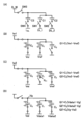
具体的には、図4に図示するように信号W1を画素に保持した後、その他の信号を書き込まない構成では、信号W1を可変(=variable)とし、その他の信号を固定あるいは書き込まない(=0)にすることで、信号W1に基づく画像を表示することができる。あるいは、信号W1、W2を可変(=variable)とし、その他の信号を固定あるいは書き込まない(=0)にすることで、信号W1、W2に基づく画像、つまり2つの画像を重ねあわせた表示をすることができる。あるいは、信号W1、W2、data_1を可変(=variable)とし、その他の信号を固定あるいは書き込まない(=0)にすることで、信号W1、W2、data_1に基づく画像、つまり3つの画像を重ねあわせた表示をすることができる。あるいは、信号W1、W2、data_1、data_2を可変(=variable)とすることで、信号W1、W2、data_1、data_2に基づく画像、つまり4つの画像を重ねあわせた表示をすることができる。なお信号W1、W2はメモリ回路112およびメモリ回路113に保持される信号のため、更新頻度の小さい画像データに基づく信号であることが好ましい。Specifically, as shown in FIG. 4, after the signal W1 is held in the pixel, in a configuration in which no other signals are written, the signal W1 is made variable and the other signals are fixed or not written. By setting (=0), an image based on the signal W1 can be displayed. Alternatively, by making the signals W 1 and W 2 variable and setting the other signals to be fixed or not written (=0), an image based on the signals W 1 and W 2 , that is, two images are superimposed. can be displayed. Alternatively, by making the signals W 1 , W 2 and data_1 variable and the other signals fixed or not written (=0), an image based on the signals W 1 , W 2 and data_1, that is, three Images can be superimposed and displayed. Alternatively, by making the signals W 1 , W 2 , data_1, and data_2 variable, it is possible to display an image based on the signals W 1 , W 2 , data_1, and data_2, that is, four images superimposed. can. Note that since the signals W 1 and W 2 are signals held in the
より具体的な構成例について図5、図6を参照して説明する。図5、図6では、画像データによって表示装置に表示される画像、および画像内で表示される表示物を用いて本発明の一態様の表示装置について説明する。図5、図6では、上記説明における信号の重ねあわせを、画像の重ねあわせとして説明する。 A more specific configuration example will be described with reference to FIGS. 5 and 6. FIG. 5 and 6, a display device of one embodiment of the present invention is described using an image displayed on the display device based on image data and a display object displayed in the image. 5 and 6, the superimposition of signals in the above description will be explained as the superimposition of images.
図5(A)には、画像160を図示している。画像160には、表示物161、表示物162、表示物163、および表示物164を図示している。また、図5(B)乃至(E)には、画像160A乃至160Dを図示している。画像160A乃至160Dは、図示するように、図5(A)で図示した表示物161乃至164が別々に表示された画像である。本発明の一態様の表示装置は、メモリ回路に保持させた信号W1、W2と、その後に書き込む信号data_1、data_2を用いることで、最大4枚の画像を重ねあわせて表示することができる。例えば、図5(B)、(C)に図示する画像160Aおよび160Bをメモリ回路112およびメモリ回路113に保持する信号W1およびW2によって予め保持しておき、信号data_1および信号data_2として図5(D)、(E)に図示する画像160Cおよび160Dを書き込むことで所望の画像である図5(A)の画像160を重ねあわせて表示することができる。An
また別の画像として、図5(F)には画像170を図示している。画像170には、表示物161、表示物162、表示物171、および表示物172を図示している。また、図5(G)および(H)には、画像170Aおよび170Bを図示している。画像170Aおよび170Bは、図示するように、図5(F)で図示した表示物171および172が別々に表示された画像である。本発明の一態様の表示装置は、メモリ回路に保持させた信号W1、W2と、その後に書き込む信号data_1、data_2を用いることで、最大4枚の画像を重ねあわせて表示することができる。例えば、図5(B)、(C)に図示する画像160Aおよび160Bをメモリ回路112およびメモリ回路113に保持する信号W1およびW2によって予め保持しておき、信号data_1および信号data_2として図5(G)、(H)に図示する画像170Aおよび170Bを書き込むことで所望の画像である図5(F)の画像170を重ねあわせて表示することができる。メモリ回路112およびメモリ回路113に保持する信号W1およびW2を用いることで、繰り返しの画像の書き込みを減らせるため、消費電力の低減に有効である。As another image, an
なお図5(A)乃至(H)で説明した例では、異なる表示物を重ねあわせて一枚の画像を表示させる構成について説明したが、本発明の一態様は他の構成においても有効である。例えば図6に図示するようにメモリ回路に保持する信号Wとして画像160Cの表示物163のように輝度が高い画像(例えば太陽の画像)の信号を保持する構成が有効である。そして後から書き込む信号dataとして画像160のように表示物161乃至164を含む信号を書き込み、重ねあわせた表示(data+W)を行うことで、得られる画像160HDの表示物163の輝度を高める(太線で輝度の向上を図示)ことができる。このように本発明の一態様は、ハイダイナミックレンジ(High-Dynamic Range:HDR)処理のような画像処理も簡便な構成で実現することができる。また重ねあわせた表示にテキストなどの情報を含めることも可能である。 Note that in the examples described with reference to FIGS. 5A to 5H, a structure in which different display objects are superimposed to display one image is described; however, one embodiment of the present invention is also effective in other structures. . For example, as shown in FIG. 6, it is effective to hold a signal of a high luminance image (for example, an image of the sun) such as the
次に、画素111の変形例について説明する。画素111は、図7(A)に示す画素111Aの構成とすることもできる。画素111Aは、画素111からトランジスタ122を省いた構成である。 Next, modified examples of the
前述したように、トランジスタ122はノードNMに書き込む信号がトランジスタ120のしきい値電圧(Vth)以上である場合に起こる不具合を解消するために設けられる。ただし、ノードNMに書き込まれる信号がVthより低い値に限定されていればトランジスタ122を省くことができる。As described above,
また、画素111は、図7(B)に示す画素111Bの構成とすることもできる。画素111Bは、それぞれのトランジスタにバックゲートを設けた構成を有する。当該バックゲートはフロントゲートと電気的に接続されており、オン電流を高める効果を有する。また、バックゲートにフロントゲートと異なる定電位を供給できる構成としてもよい。当該構成とすることで、トランジスタのしきい値電圧を制御することができる。なお、図7(B)においては、全てのトランジスタにバックゲートを設けた構成を図示しているが、バックゲートが設けられないトランジスタを有していてもよい。また、トランジスタがバックゲートを有する構成は、本実施の形態における他の画素回路にも有効である。 Alternatively, the
また、画素111は、図8(A)に示す画素111Cの構成とすることもできる。画素111Cの回路は、メモリ回路として機能するトランジスタ125および容量素子126を追加した構成である。画素111に追加した当該メモリ回路には、配線DL_3を介して信号が与えられる。図8(A)のようにメモリ回路を追加することで、3つ以上のメモリ回路を備えた画素を有する表示装置とすることができる。 Alternatively, the
また、画素111は、図8(B)に示す画素111Dの構成とすることもできる。画素111Dでは、配線GL_1の機能を配線GL_1Aおよび配線GL_1Bに分け、トランジスタ117およびトランジスタ118、トランジスタ121および追加したトランジスタ127を別々の信号で制御する構成を有する。当該構成とすることで、複数のメモリ回路に保持された信号を選択して画像の重ねあわせに用いることが可能になる。 Alternatively, the
図9(A)には、図1(A)で図示したブロック図の構成に加えて、信号変換回路150およびメモリ回路151を図示している。 FIG. 9A shows a
表示装置100で複数の画像を重ねあわた表示する場合、画素111内のメモリ回路112、113に保持するための信号W1、W2は、信号変換回路150でメモリ回路151を参照して変換し、表示装置100に出力する構成が好ましい。When a plurality of images are superimposed and displayed on the
また上記説明では、画素111について説明したが、カラー表示を行う場合、画素111は図9(B)に図示するようにRGB(赤、緑、青)の3原色の副画素111R、111G、111Bのそれぞれに相当し、複数の副画素を組み合わせて、ひとつの画素を構成する。なお副画素の数は、図9(B)に図示するRGBの3つに限らず、図9(C)に図示するようにRGBW(赤、緑、青、白)の副画素111R、111G、111B、111Wを組み合わせて、ひとつの画素を構成することも有効である。 In the above description, the
本実施の形態は、他の実施の形態等に記載した構成と適宜組み合わせて実施することが可能である。 This embodiment can be implemented in appropriate combination with the structures described in other embodiments and the like.
(実施の形態2)
本実施の形態では、上記実施の形態1で説明した構成とは異なる表示装置の構成例について図面を参照して説明する。本実施の形態では、上記実施の形態1と異なる点について詳細に説明し、重複する記載については説明を省略する場合がある。(Embodiment 2)
In this embodiment mode, a structural example of a display device which is different from the structure described in
図10には、図1(A)の画素111に適用可能な画素111Eの構成例について図示する。画素111Eは、トランジスタM1、トランジスタM2、トランジスタM4、トランジスタM5、容量素子C1、容量素子C2、容量素子C3、および発光素子OLEDを有する。また図10では、トランジスタM2のゲートが接続されるノードを、ノードNMとして図示している。なお図10に図示するトランジスタは、いずれもnチャネル型のトランジスタを図示しているが、pチャネル型を用いることもできる。 FIG. 10 illustrates a configuration example of a
トランジスタM2は、発光素子OLEDに流す電流量を制御する機能を有する。トランジスタM2以外のトランジスタは、スイッチとしての機能を有する。メモリ回路MEM1は容量素子C1、トランジスタM1、およびトランジスタM4を有する。メモリ回路MEM2は容量素子C2、トランジスタM4、およびトランジスタM5を有する。 The transistor M2 has a function of controlling the amount of current that flows through the light emitting element OLED. Transistors other than the transistor M2 function as switches. The memory circuit MEM1 has a capacitive element C1, a transistor M1, and a transistor M4. The memory circuit MEM2 has a capacitive element C2, a transistor M4, and a transistor M5.
また図10では、図1(A)で図示した配線GLとして、配線GL_1、配線GL_2、および配線GL_3を図示している。配線GL_1、配線GL_2、および配線GL_3は、スイッチとして機能するトランジスタのオンまたはオフを制御するための信号を画素111Eに伝える機能を有する。 In FIG. 10, a wiring GL_1, a wiring GL_2, and a wiring GL_3 are illustrated as the wirings GL illustrated in FIG. The wiring GL_1, the wiring GL_2, and the wiring GL_3 have a function of transmitting a signal for controlling on/off of a transistor functioning as a switch to the
また図10では、図1(A)で図示した配線DLとして、配線DL_1、配線DL_2、および配線DL_Wを図示している。配線DL_1、配線DL_2は、画像の表示を行うための信号および参照電圧を画素111Eに伝える機能を有する。配線DL_Wは、画像の表示を行うための信号を画素111Eに伝える機能を有する。 In FIG. 10, a wiring DL_1, a wiring DL_2, and a wiring DL_W are illustrated as the wirings DL illustrated in FIG. The wiring DL_1 and the wiring DL_2 have a function of transmitting a signal and a reference voltage for displaying an image to the
容量素子C1または容量素子C2は、メモリ回路MEM1またはメモリ回路MEM2に書き込まれる信号を電荷として保持する機能を有する。容量素子C1または容量素子C2の一方の電極または他方の電極に電気的に接続されるトランジスタM1、トランジスタM4、およびトランジスタM5は、オンとすることで、容量素子C1または容量素子C2の電極に信号に応じた電荷を与える機能を有する。またトランジスタM1、トランジスタM4、およびトランジスタM5は、オフとすることで、容量素子C1または容量素子C2の電極に電荷を保持する機能を有する。またトランジスタM1、トランジスタM4、およびトランジスタM5は、オフとすることで、容量素子C1または容量素子C2の一方の電極のノードを電気的に浮遊状態(フローティング)にする機能を有する。 The capacitor C1 or C2 has a function of holding a signal written to the memory circuit MEM1 or the memory circuit MEM2 as charge. By turning on the transistor M1, the transistor M4, and the transistor M5, which are electrically connected to one electrode or the other electrode of the capacitor C1 or the capacitor C2, a signal is applied to the electrode of the capacitor C1 or the capacitor C2. It has the function of giving an electric charge according to In addition, the transistor M1, the transistor M4, and the transistor M5 have a function of holding electric charge in the electrode of the capacitor C1 or the capacitor C2 by being turned off. The transistor M1, the transistor M4, and the transistor M5 have a function of electrically floating the node of one electrode of the capacitor C1 or the capacitor C2 by being turned off.
図10に図示するように、容量素子C1の一方の電極は、トランジスタM1を介して配線DL_1と接続される。容量素子C1の他方の電極は、トランジスタM4を介して配線DL_Wと接続される。容量素子C2の一方の電極は、トランジスタM5を介して配線DL_2と接続される。容量素子C2の他方の電極は、トランジスタM4を介して配線DL_Wと接続される。 As illustrated in FIG. 10, one electrode of the capacitor C1 is connected to the wiring DL_1 through the transistor M1. The other electrode of the capacitor C1 is connected to the wiring DL_W through the transistor M4. One electrode of the capacitor C2 is connected to the wiring DL_2 through the transistor M5. The other electrode of the capacitor C2 is connected to the wiring DL_W through the transistor M4.
トランジスタM1、トランジスタM4、およびトランジスタM5は、オフ時に流れる電流(オフ電流)が低いことが好適である。極めてオフ電流の低いトランジスタを用いることで、ノードNMの電位を長時間保持することができる。当該トランジスタには、例えば、OSトランジスタを用いることができる。 It is preferable that the transistor M1, the transistor M4, and the transistor M5 have low current (off current) when they are off. By using a transistor with extremely low off-state current, the potential of the node NM can be held for a long time. For example, an OS transistor can be used as the transistor.
容量素子C3は、トランジスタM2のゲートとソースとの間の電圧を保持する機能を有する。容量素子C3の一方の電極は、トランジスタM2のゲートと接続される。容量素子C3の他方の電極は、トランジスタM2のソース又はドレインの一方の電極(ソース側)と接続される。トランジスタM2のソースまたはドレインの他方(ドレイン側)は、配線ANOに接続される。配線ANOは、発光素子OLEDに電流を流すための電圧が与えられる。配線ANOは、電流供給線、あるいはアノード線としての機能を有する。なおトランジスタM2のソース又はドレインの一方は、固定電位が与えられた配線との間でスイッチとして機能するトランジスタが設けられることが好適である。当該構成とすることで、信号の書き込み期間において、トランジスタM2のソース又はドレインの一方における電位の変動を抑制することができる。 The capacitor C3 has a function of holding the voltage between the gate and source of the transistor M2. One electrode of the capacitive element C3 is connected to the gate of the transistor M2. The other electrode of the capacitor C3 is connected to one electrode (source side) of the source or drain of the transistor M2. The other (drain side) of the source and drain of the transistor M2 is connected to the wiring ANO. The wiring ANO is supplied with a voltage for causing current to flow through the light emitting element OLED. The wiring ANO functions as a current supply line or an anode line. Note that one of the source and the drain of the transistor M2 is preferably provided with a transistor functioning as a switch with a wiring to which a fixed potential is applied. With this structure, variation in the potential of one of the source and the drain of the transistor M2 can be suppressed in the signal writing period.
発光素子OLEDの一方の電極は、トランジスタM2のソースまたはドレインの一方(ソース側)に接続される。発光素子OLEDの他方の電極は、配線CATに接続される。配線CATは、共通電位線、あるいはカソード線としての機能を有する。なお発光素子OLEDは、流れる電流量に応じて輝度の制御が可能な表示素子であり、例えば有機EL素子を適用することができる。なおトランジスタM2のソースまたはドレインの一方と、発光素子OLEDの一方の電極の間には、非発光期間以外に発光素子OLEDに電流が流れて発光してしまうのを防ぐためにスイッチとして機能するトランジスタが設けられることが好適である。なお有機EL素子等の発光素子以外の表示素子としては、液晶素子を用いることも可能である。 One electrode of the light emitting element OLED is connected to one of the source and the drain (source side) of the transistor M2. The other electrode of the light emitting element OLED is connected to the wiring CAT. The wiring CAT functions as a common potential line or a cathode line. Note that the light emitting element OLED is a display element whose luminance can be controlled according to the amount of current that flows, and for example, an organic EL element can be applied. Note that a transistor functioning as a switch is provided between one of the source and drain of the transistor M2 and one electrode of the light-emitting element OLED to prevent current from flowing to the light-emitting element OLED and emitting light during periods other than the non-light-emitting period. is preferably provided. A liquid crystal element can also be used as a display element other than a light-emitting element such as an organic EL element.
本発明の一態様は、ソースドライバ140から出力される階調表示を行うための信号を画素に供給して複数のメモリ回路にそれぞれ保持しておき、複数のメモリ回路に保持した信号とは別の階調表示を行うための信号をソースドライバ140から画素に供給する。図10では、2つのメモリ回路にソースドライバ140から出力される階調表示を行うための信号をそれぞれ保持しておき、階調表示を行うための信号をソースドライバ140から配線DL_1および配線DL_2を介して画素に供給する構成とする。 In one embodiment of the present invention, a signal for performing gradation display output from the
当該構成とすることで、予め2つの信号が保持されたメモリ回路に、別の2つの信号が付加された4つの信号に基づいて、発光素子に流れる電流を制御する構成とすることができる。したがって、当該画素を備えた表示部では、4つの信号に基づく表示を行うことができる。これにより画素内の2つのメモリ回路にそれぞれ、ソースドライバが出力可能なビット数(例えば8bit:256階調)の信号を保持させることができるのに加えて、後から画素に書き込む2つの信号のそれぞれをソースドライバが出力可能なビット数(例えば8bit:256階調)の信号を画素に書き込む構成を実現することができる。そのため、4つの信号の階調数の合計である256+256+256+256=1024相当の階調数(10bit)の信号、つまりソースドライバが出力可能なビット数以上の階調数の書き込みによる表示を行う構成とすることができる。当該構成では、ソースドライバ等が生成可能な電位より高い電位の画像信号に対応する画像を表示装置で表示することができるため、表示装置のダイナミックレンジを高めることができる。 With this structure, the current flowing through the light-emitting element can be controlled based on four signals in which two signals are added to a memory circuit in which two signals are held in advance. Therefore, a display portion including the pixel can perform display based on four signals. This allows each of the two memory circuits in the pixel to hold a signal of the number of bits that the source driver can output (for example, 8 bits: 256 gradations). It is possible to realize a configuration in which a signal of the number of bits (for example, 8 bits: 256 gradations) that can be output by the source driver is written to the pixel. Therefore, display is performed by writing a signal with a number of gradations (10 bits) equivalent to 256+256+256+256=1024, which is the total number of gradations of the four signals, that is, a number of gradations greater than the number of bits that the source driver can output. be able to. With this structure, the display device can display an image corresponding to an image signal having a potential higher than the potential that can be generated by the source driver or the like; therefore, the dynamic range of the display device can be increased.
図11(A)、(B)に示すタイミングチャートおよび図12(A)乃至(D)に示す回路図を用いて、画素111Eの駆動方法の一例を説明する。図11(A)では、メモリ回路MEM1およびメモリ回路MEM2に保持させる信号の書き込み動作について、図11(B)では、メモリ回路MEM1およびメモリ回路MEM2に保持された信号に、別の信号を付加して表示を行う際の動作について図示している。なお図11(A)、(B)に示すタイミングチャートでは、配線GL_1乃至GL_3、DL_1、DL_2およびDL_Wに与える信号波形を図示している。 An example of a method for driving the
なお、配線DL_Wに供給される信号をW1、W2とし、信号によってメモリ回路MEM1に保持される電圧をVw1、信号によってメモリ回路MEM2に保持される電圧をVw2とする。また、メモリ回路MEM1に電圧Vw1を保持した状態で配線DL_1を介して画素111Eに書き込まれる信号をdata1とし、信号によってメモリ回路MEM1に付加される電圧をVdata1とする。また、メモリ回路MEM2に電圧Vw2を保持した状態で配線DL_2を介して画素111Eに書き込まれる信号をdata2とし、信号によってメモリ回路MEM2に付加される電圧をVdata2とする。 Note that the signals supplied to the wirings DL_W are W1 and W2, the voltage held in the memory circuit MEM1 by the signals is Vw1, and the voltage held in the memory circuit MEM2 by the signals is Vw2. A signal written to the
まず、図11(A)を用いてメモリ回路MEM1およびメモリ回路MEM2に保持させる信号W1、W2の書き込み動作を説明する。また図11(A)、(B)の動作の説明については、説明を簡略化するため、図12(A)乃至(D)の回路図を参照して説明する。図12(A)乃至(D)は、図10の回路図の主要部について抜き出して示したものである。図12(A)では、図10に対応する構成としてスイッチとして機能するトランジスタをスイッチSW1乃至SW4、容量素子C1、C2、C3を図示している。なお容量素子C1、C2、C3の容量(キャパシタンス)はC1,C2,C3として図示する。スイッチSW1乃至SW3は、図10におけるトランジスタM1、トランジスタM4、トランジスタM5に相当する。スイッチSW4は、信号書き込み時に、トランジスタM2のソース又はドレインの一方における電位の変動を抑制するためのスイッチである。スイッチSW4は、信号書き込み時にオンとするスイッチである。スイッチSW4に接続される配線LELは、固定電位Velを与える配線である。First, the write operation of the signals W1 and W2 held in the memory circuit MEM1 and the memory circuit MEM2 is described with reference to FIG. 11A and 11B will be described with reference to the circuit diagrams of FIGS. 12A to 12D in order to simplify the description. FIGS. 12A to 12D show the main parts extracted from the circuit diagram of FIG. FIG. 12A illustrates transistors functioning as switches as switches SW1 to SW4 and capacitors C1, C2, and C3 as a structure corresponding to FIG. Note that the capacitances of the capacitive elements C1, C2 and C3 are illustrated as C1 , C2 and C3 . The switches SW1 to SW3 correspond to the transistor M1, transistor M4, and transistor M5 in FIG. The switch SW4 is a switch for suppressing potential fluctuation at one of the source and the drain of the transistor M2 during signal writing. A switch SW4 is a switch that is turned on when a signal is written. A wiring LEL connected to the switch SW4 is a wiring for applying a fixed potential Vel.
メモリ回路MEM1およびメモリ回路MEM2に信号W1、W2に基づく電圧Vw1、Vw2を書き込む場合、まずは配線DL_Wを電圧Vw1とし、配線DL_1をVref(参照電圧)とした状態とする。配線DL_2の電位は特に設定されない。なお配線DL_1に与えるVrefは、Vw1-Vrefが正の値となるように値を決めておくことが好ましい。各配線の電位を所定の電圧に設定した状態で、図11(A)の時刻T1のように、配線GL_1、配線GL_3に与える信号をHレベルとする。つまり図12(B)に図示するようにスイッチSW1、SW3、SW4をオンにする。すると、容量素子C1の両端の電極には電圧Vref、Vw1が印加される。このとき容量素子C1のノードNM側の電極に蓄積される電荷量をQ1とすると式(9)のようになる。 When voltages Vw1 and Vw2 based on the signals W1 and W2 are written to the memory circuit MEM1 and the memory circuit MEM2, first, the wiring DL_W is set to the voltage Vw1 and the wiring DL_1 is set to Vref (reference voltage). The potential of the wiring DL_2 is not particularly set. Note that Vref applied to the wiring DL_1 is preferably determined so that Vw1-Vref is a positive value. With the potential of each wiring set to a predetermined voltage, the signal supplied to the wiring GL_1 and the wiring GL_3 is set to H level at time T1 in FIG. That is, the switches SW1, SW3, and SW4 are turned on as shown in FIG. 12(B). Then, voltages Vref and Vw1 are applied to the electrodes at both ends of the capacitive element C1. Assuming that the amount of charge accumulated in the electrode of the capacitive element C1 on the node NM side at this time is Q1, Equation (9) is obtained.
Q1=C1(Vw1-Vref)(9)Q1=C 1 (Vw1-Vref) (9)
次いで配線DL_Wを電圧Vw2とし、配線DL_2をVrefとした状態とする。配線DL_1の電位は特に設定されない。なお配線DL_2に与えるVrefは、Vw2-Vrefが正の値となるように値を決めておくことが好ましい。各配線の電位を所定の電圧に設定した状態で、図11(A)の時刻T2のように、配線GL_2、配線GL_3に与える信号をHレベルとする。つまり図12(C)に図示するようにスイッチSW2、SW3、SW4をオンにする。すると、容量素子C2の両端の電極には電圧Vref、Vw2が印加される。このとき容量素子C2のノードNM側の電極に蓄積される電荷量をQ2とすると式(10)のようになる。 Next, the wiring DL_W is set to the voltage Vw2, and the wiring DL_2 is set to Vref. The potential of the wiring DL_1 is not particularly set. Note that Vref applied to the wiring DL_2 is preferably determined so that Vw2-Vref is a positive value. With the potential of each wiring set to a predetermined voltage, the signals supplied to the wirings GL_2 and GL_3 are set to H level at time T2 in FIG. That is, the switches SW2, SW3, and SW4 are turned on as shown in FIG. 12(C). Then, voltages Vref and Vw2 are applied to the electrodes at both ends of the capacitive element C2. Assuming that the amount of charge accumulated in the electrode of the capacitive element C2 on the node NM side at this time is Q2, Equation (10) is obtained.
Q2=C2(Vw2-Vref)(10) Q2=C2(Vw2-Vref) (10)
時刻T2、つまり図12(C)の状態では、スイッチSW1はオフである。そのため、容量素子C1の一方の電極のノード(図12(C)のノードNr1)は、電気的に浮遊状態であり、電荷保存則が成り立つ。そのため、時刻T2、つまり図12(C)の状態では、容量素子C2の両端の電極に保持される電荷量Q1は、式(9)と同様に保持され続ける。At time T2, that is, in the state of FIG. 12(C), the switch SW1 is off. Therefore, the node of one electrode of the capacitor C1 (the node N r1 in FIG. 12C) is in an electrically floating state, and the law of conservation of charge is satisfied. Therefore, at time T2, that is, in the state of FIG. 12C, the charge amount Q1 held in the electrodes at both ends of the capacitive element C2 continues to be held in the same manner as in Equation (9).
なお図11(A)に図示する時刻T1、T2における信号W1、W2の書き込みは、フレーム期間毎に分けて書き込んでもよいし、1水平走査期間内に1値ずつ書き込む動作としてもよい。 The signals W1 and W2 at times T1 and T2 shown in FIG. 11A may be written separately for each frame period, or may be written one value at a time during one horizontal scanning period.
次いで図11(B)を用いてメモリ回路MEM1およびメモリ回路MEM2に信号W1、W2に基づく電圧Vw1、電圧Vw2を保持した状態で配線DL_1、DL_2を介して画素111Eに信号data1、data2を付加する動作を説明する。 Next, with reference to FIG. 11B, the signals data1 and data2 are applied to the
メモリ回路MEM1およびメモリ回路MEM2に信号data1、data2を書き込む場合、配線DL_1をVdata1とし、配線DL_2をVdata2とし、配線DL_WをVSS等のLレベルとした状態で、配線GL_1、GL_2に与える信号をHレベル、配線GL_3に与える信号をLレベルとする。つまり図12(D)に図示するようにスイッチSW1、SW2、SW4をオンにし、スイッチSW3をオフにする。すると、容量素子C1,C2,C3の一方の電極が電気的に浮遊状態となり、容量素子C1,C2の他方の電極の電圧がVw1、Vw2からVdata1、Vdata2にそれぞれ変化する。ノードNMの電圧をVgとし、容量素子C1でのノードNM側の電極に蓄積される電荷量をQ1’とすると、式(11)のようになる。Vgは容量結合によって変化する電圧である。 When the signals data1 and data2 are written to the memory circuit MEM1 and the memory circuit MEM2, the wiring DL_1 is set to Vdata1, the wiring DL_2 is set to Vdata2, and the wiring DL_W is set to L level such as VSS. A signal applied to the wiring GL_3 is set to L level. That is, as shown in FIG. 12(D), the switches SW1, SW2, and SW4 are turned on, and the switch SW3 is turned off. Then, one electrodes of the capacitive elements C1, C2 and C3 are electrically floating, and the voltages of the other electrodes of the capacitive elements C1 and C2 change from Vw1 and Vw2 to Vdata1 and Vdata2, respectively. Assuming that the voltage of the node NM is Vg and the amount of charge accumulated in the electrode of the capacitive element C1 on the node NM side is Q1', Equation (11) is obtained. Vg is a voltage that changes due to capacitive coupling.
Q1’=C1(Vdata1-Vg)(11)Q1′=C 1 (Vdata1−Vg) (11)
同様にしてこのとき容量素子C2、容量素子C3のノードNM側の電極に蓄積される電荷量をQ2’、Q3’とすると式(12)、(13)のようになる。 Similarly, if the amounts of charge accumulated in the electrodes of the capacitive elements C2 and C3 on the node NM side at this time are Q2' and Q3', equations (12) and (13) are obtained.
Q2’=C2(Vdata2-Vg)(12)Q2′=C 2 (Vdata2−Vg) (12)
Q3’=C3(Vg-Vel)(13)Q3′=C 3 (Vg−Vel) (13)
図11(A)と図11(B)の動作の間でノードNMでは、スイッチSW1乃至SW4のオフ電流が極めて低いため、電荷保存側が成り立つ。つまり式(7)が成り立つ。 At the node NM between the operations in FIGS. 11A and 11B, the off-state current of the switches SW1 to SW4 is extremely low, so the charge storage side is established. That is, the formula (7) holds.
Q1+Q2+Q3=Q1’+Q2’+Q3’(7) Q1+Q2+Q3=Q1'+Q2'+Q3' (7)
式(7)をVgについて解くと、式(14)が成り立つ。なお式(14)では簡略化のため、電圧Vw1、Vw2、Vdata1、Vdata2に対し、参照電圧VrefおよびVelを0Vとし、容量C1とC2とが等しいとし、容量C3が容量C1およびC2に対して十分小さいものとしている。Solving equation (7) for Vg yields equation (14). For simplification in equation (14), with respect to voltages Vw1, Vw2, Vdata1, and Vdata2, the reference voltages Vref and Vel are assumed to be 0 V, the capacitances C1 and C2 are equal, and the capacitance C3 is equal to the capacitances C1 and C2 . It is assumed to be sufficiently small with respect to C2 .
[数2][Number 2]
式(14)から電圧Vgは、電圧Vw1、電圧Vw2、電圧Vdata1、電圧Vdata2を合算した値で得られるため、メモリ回路に保持した信号と、後から書き込む信号と、の足しあわせ(足し算)を行うことができる。なお電圧Vw1、電圧Vw2、電圧Vdata1、電圧Vdata2は、負の値となるよう信号を書き込むことで、信号の足しあわせに加えて、信号の引き算を行うことも可能である。 From equation (14), the voltage Vg is obtained by adding the voltage Vw1, the voltage Vw2, the voltage Vdata1, and the voltage Vdata2. It can be carried out. Note that by writing signals so that the voltage Vw1, the voltage Vw2, the voltage Vdata1, and the voltage Vdata2 have negative values, the signals can be added and subtracted.
本発明の一態様の表示装置は、メモリ回路に保持させた信号W1、W2と、その後に書き込む信号data1、data2を用いることで、最大4つの信号に基づいて、発光素子に流れる電流を制御する構成とすることができる。したがって、当該画素を備えた表示部では、4つの信号に基づく表示を行うことができる。これにより画素内の2つのメモリ回路にそれぞれ、ソースドライバが出力可能なビット数(例えば8bit:256階調)の信号を保持させることができるのに加えて、後から画素に書き込む2つの信号のそれぞれをソースドライバが出力可能なビット数(例えば8bit:256階調)の信号を画素に書き込む構成を実現することができる。そのため、4つの信号の階調数の合計である256+256+256+256=1024相当の階調数(10bit)の信号、つまりソースドライバが出力可能なビット数以上の階調数の書き込みによる表示を行う構成とすることができる。当該構成では、ソースドライバ等が生成可能な電位より高い電位の画像信号に対応する画像を表示装置で表示することができるため、表示装置のダイナミックレンジを高めることができる。 The display device of one embodiment of the present invention uses the signals W1 and W2 held in the memory circuit and the signals data1 and data2 to be written afterward, thereby controlling the current flowing through the light-emitting element based on up to four signals. can be configured. Therefore, a display portion including the pixel can perform display based on four signals. This allows each of the two memory circuits in the pixel to hold a signal of the number of bits that the source driver can output (for example, 8 bits: 256 gradations). It is possible to realize a configuration in which a signal of the number of bits (for example, 8 bits: 256 gradations) that can be output by the source driver is written to the pixel. Therefore, display is performed by writing a signal with a number of gradations (10 bits) equivalent to 256+256+256+256=1024, which is the total number of gradations of the four signals, that is, a number of gradations greater than the number of bits that the source driver can output. be able to. With this structure, the display device can display an image corresponding to an image signal having a potential higher than the potential that can be generated by the source driver or the like; therefore, the dynamic range of the display device can be increased.
上記説明した本発明の一態様の表示装置による効果について、図13に図示するグラフを用いて説明する。図13に示すグラフは、横軸が階調数、縦軸が出力、具体的には発光素子の輝度を表している。 Effects of the above-described display device of one embodiment of the present invention are described with reference to graphs in FIGS. In the graph shown in FIG. 13, the horizontal axis represents the number of gradations and the vertical axis represents the output, specifically the luminance of the light emitting element.
上述したように本発明の一態様の構成では、最大4つの信号に基づいて、発光素子に流れる電流を制御する構成とすることができる。例えば信号W1がソースドライバの出力可能なビット数である8ビットで書き込まれた場合、当該信号W1だけでは256値の階調数しか表現できないが、信号W2、data1、data2といったソースドライバの出力可能なビット数である8ビットの信号と組み合わせて表現可能な階調数を増やすことにより、最大1024階調、つまり10bit相当のビット数で表示することが可能となる。As described above, in the structure of one embodiment of the present invention, the current flowing through the light-emitting element can be controlled based on up to four signals. For example, when the signal W1 is written in 8 bits, which is the number of bits that the source driver can output, only the signal W1 can express only 256 gradation levels. By increasing the number of gradations that can be expressed in combination with an 8-bit signal that can be output, it is possible to display with a maximum of 1024 gradations, that is, the number of bits equivalent to 10 bits.
次に、画素111Eの変形例について説明する。画素111Eは、図14(A)に示す画素111Fの構成とすることもできる。画素111Fは、画素111EにトランジスタM3およびM6を追加した構成である。 Next, a modified example of the
トランジスタM3およびM6は、配線VLと、トランジスタM2のソースまたはドレインの一方(ソース側)との間の導通状態を制御するスイッチとしての機能を有する。トランジスタM3のゲートは、配線GL_1と接続される。トランジスタM3のソースまたはドレインの一方は、トランジスタM2のソース又はドレインの一方と接続される。トランジスタM3のソースまたはドレインの他方は、配線VLと接続される。トランジスタM6のゲートは、配線GL_2と接続される。トランジスタM6のソースまたはドレインの一方は、トランジスタM2のソース又はドレインの一方と接続される。トランジスタM6のソースまたはドレインの他方は、配線VLと接続される。なお配線VLは、定電位、例えば上述した電圧Velを与えるための配線である。また配線VLは、トランジスタM2に流れる電流を外部に出力するための機能を有する構成としてもよい。当該構成とすることで、定期的にトランジスタM2に流れる電流をモニターすることができるため、トランジスタM2のばらつきに応じた補正を行うことができる。 The transistors M3 and M6 function as switches that control conduction between the wiring VL and one of the source and the drain (source side) of the transistor M2. A gate of the transistor M3 is connected to the wiring GL_1. One of the source and drain of the transistor M3 is connected to one of the source and drain of the transistor M2. The other of the source and drain of the transistor M3 is connected to the wiring VL. A gate of the transistor M6 is connected to the wiring GL_2. One of the source and drain of the transistor M6 is connected to one of the source and drain of the transistor M2. The other of the source and drain of the transistor M6 is connected to the wiring VL. Note that the wiring VL is a wiring for applying a constant potential, for example, the voltage Vel described above. Further, the wiring VL may have a function of outputting the current flowing through the transistor M2 to the outside. With such a structure, the current flowing through the transistor M2 can be monitored periodically, so that the variation in the transistor M2 can be corrected.
また、図14(A)に図示する画素111Fは、図14(B)に示す画素111Gの構成とすることもできる。画素111Gは、図14(A)に図示する画素111Fのそれぞれのトランジスタにバックゲートを設けた構成を有する。当該バックゲートはフロントゲートと電気的に接続されており、オン電流を高める効果を有する。また、バックゲートにフロントゲートと異なる定電位を供給できる構成としてもよい。当該構成とすることで、トランジスタのしきい値電圧を制御することができる。なお、図14(B)においては、全てのトランジスタにバックゲートを設けた構成を図示しているが、バックゲートが設けられないトランジスタを有していてもよい。 The
本実施の形態は、他の実施の形態等に記載した構成と適宜組み合わせて実施することが可能である。 This embodiment can be implemented in appropriate combination with the structures described in other embodiments and the like.
(実施の形態3)
本実施の形態では、実施の形態1および2で説明したOSトランジスタの詳細について説明する。(Embodiment 3)
In this embodiment, details of the OS transistor described in
OSトランジスタに用いる半導体材料としては、エネルギーギャップが2eV以上、好ましくは2.5eV以上、より好ましくは3eV以上である金属酸化物を用いることができる。代表的には、インジウムを含む酸化物半導体等であり、例えば、後述するCAAC-OS又はCAC-OS等を用いることができる。CAAC-OSは結晶を構成する原子が安定であり、信頼性を重視するトランジスタ等に適する。また、CAC-OSは、高移動度特性を示すため、高速駆動を行うトランジスタ等に適する。 As a semiconductor material used for an OS transistor, a metal oxide with an energy gap of 2 eV or more, preferably 2.5 eV or more, more preferably 3 eV or more can be used. Typically, an oxide semiconductor containing indium or the like is used, and for example, CAAC-OS, CAC-OS, or the like, which will be described later, can be used. CAAC-OS has stable atoms forming crystals, and is suitable for transistors and the like in which reliability is important. In addition, since CAC-OS exhibits high mobility characteristics, it is suitable for transistors and the like that are driven at high speed.
OSトランジスタはエネルギーギャップが大きいため、極めて低いオフ電流特性を示す。また、OSトランジスタは、インパクトイオン化、アバランシェ降伏、及び短チャネル効果等が生じない等Siトランジスタとは異なる特徴を有し、信頼性の高い回路を形成することができる。 Since the OS transistor has a large energy gap, it exhibits extremely low off-current characteristics. In addition, the OS transistor has characteristics different from the Si transistor, such as impact ionization, avalanche breakdown, short channel effect, and the like, and can form a highly reliable circuit.
OSトランジスタが有する半導体層は、例えばインジウム、亜鉛及びM(アルミニウム、チタン、ガリウム、ゲルマニウム、イットリウム、ジルコニウム、ランタン、セリウム、スズ、ネオジム又はハフニウム等の金属)を含むIn-M-Zn系酸化物で表記される膜とすることができる。 The semiconductor layer of the OS transistor is, for example, an In--M--Zn oxide containing indium, zinc, and M (a metal such as aluminum, titanium, gallium, germanium, yttrium, zirconium, lanthanum, cerium, tin, neodymium, or hafnium). It can be a film represented by
半導体層を構成する酸化物半導体がIn-M-Zn系酸化物の場合、In-M-Zn酸化物を成膜するために用いるスパッタリングターゲットの金属元素の原子数比は、In≧M、Zn≧Mを満たすことが好ましい。このようなスパッタリングターゲットの金属元素の原子数比として、In:M:Zn=1:1:1、In:M:Zn=1:1:1.2、In:M:Zn=3:1:2、In:M:Zn=4:2:3、In:M:Zn=4:2:4.1、In:M:Zn=5:1:6、In:M:Zn=5:1:7、In:M:Zn=5:1:8等が好ましい。なお、成膜される半導体層の原子数比はそれぞれ、上記のスパッタリングターゲットに含まれる金属元素の原子数比のプラスマイナス40%の変動を含む。 When the oxide semiconductor constituting the semiconductor layer is an In-M-Zn-based oxide, the atomic ratio of the metal element in the sputtering target used for forming the In-M-Zn oxide is In≧M, Zn. It is preferable to satisfy ≧M. The atomic ratios of the metal elements in such a sputtering target are In:M:Zn=1:1:1, In:M:Zn=1:1:1.2, In:M:Zn=3:1: 2, In:M:Zn=4:2:3, In:M:Zn=4:2:4.1, In:M:Zn=5:1:6, In:M:Zn=5:1: 7, In:M:Zn=5:1:8, etc. are preferable. It should be noted that the atomic ratio of the semiconductor layers to be deposited includes a variation of plus or minus 40% of the atomic ratio of the metal element contained in the sputtering target.
半導体層としては、キャリア密度の低い酸化物半導体を用いる。例えば、半導体層は、キャリア密度が1×10¹⁷/cm3以下、好ましくは1×1015/cm3以下、さらに好ましくは1×1013/cm3以下、より好ましくは1×1011/cm3以下、さらに好ましくは1×1010/cm3未満であり、1×10-9/cm3以上のキャリア密度の酸化物半導体を用いることができる。そのような酸化物半導体を、高純度真性又は実質的に高純度真性な酸化物半導体と呼ぶ。これにより不純物濃度が低く、欠陥準位密度が低いため、安定な特性を有する酸化物半導体であるといえる。An oxide semiconductor with low carrier density is used for the semiconductor layer. For example, the semiconductor layer has a carrier density of 1×10 17 /cm 3 or less, preferably 1×10 15 /cm 3 or less, more preferably 1×10 13 /cm 3 or less, more preferably 1×10 11 /
なお、これらに限られず、必要とするトランジスタの半導体特性及び電気特性(電界効果移動度、しきい値電圧等)に応じて適切な組成のものを用いればよい。また、必要とするトランジスタの半導体特性を得るために、半導体層のキャリア密度や不純物濃度、欠陥密度、金属元素と酸素の原子数比、原子間距離、密度等を適切なものとすることが好ましい。 Note that the material is not limited to these, and a material having an appropriate composition may be used according to required semiconductor characteristics and electrical characteristics (field-effect mobility, threshold voltage, etc.) of the transistor. In addition, in order to obtain the required semiconductor characteristics of the transistor, it is preferable to appropriately set the carrier density, impurity concentration, defect density, atomic ratio of metal elements and oxygen, interatomic distance, density, etc. of the semiconductor layer. .
半導体層を構成する酸化物半導体において、第14族元素の一つであるシリコンや炭素が含まれると、酸素欠損が増加し、n型化してしまう。このため、半導体層におけるシリコンや炭素の濃度(二次イオン質量分析法により得られる濃度)を、2×10¹⁸atoms/cm3以下、好ましくは2×1017atoms/cm3以下とする。If silicon or carbon, which is one of Group 14 elements, is contained in an oxide semiconductor forming a semiconductor layer, oxygen vacancies increase and the oxide semiconductor becomes n-type. Therefore, the concentration of silicon or carbon in the semiconductor layer (concentration obtained by secondary ion mass spectrometry) is set to 2×10 18 atoms/cm 3 or less, preferably 2×10 17 atoms/cm 3 or less.
また、アルカリ金属及びアルカリ土類金属は、酸化物半導体と結合するとキャリアを生成する場合があり、トランジスタのオフ電流が増大してしまうことがある。このため、半導体層におけるアルカリ金属又はアルカリ土類金属の濃度(二次イオン質量分析法により得られる濃度)を、1×10¹⁸atoms/cm3以下、好ましくは2×1016atoms/cm3以下にする。Further, alkali metals and alkaline earth metals might generate carriers when bonded to an oxide semiconductor, which might increase the off-state current of a transistor. Therefore, the concentration of alkali metals or alkaline earth metals in the semiconductor layer (concentration obtained by secondary ion mass spectrometry) is 1×10 18 atoms/cm 3 or less, preferably 2×10 16 atoms/cm 3 or less. to
また、半導体層を構成する酸化物半導体に窒素が含まれていると、キャリアである電子が生じてキャリア密度が増加し、n型化しやすい。この結果、窒素が含まれている酸化物半導体を用いたトランジスタはノーマリーオン特性となりやすい。このため半導体層における窒素濃度(二次イオン質量分析法により得られる濃度)は、5×10¹⁸atoms/cm3以下にすることが好ましい。In addition, when nitrogen is contained in the oxide semiconductor forming the semiconductor layer, electrons as carriers are generated to increase the carrier density and easily become n-type. As a result, a transistor including an oxide semiconductor containing nitrogen tends to have normally-on characteristics. Therefore, the nitrogen concentration (concentration obtained by secondary ion mass spectrometry) in the semiconductor layer is preferably 5×10 18 atoms/cm 3 or less.
また、半導体層は、例えば非単結晶構造でもよい。非単結晶構造は、例えば、c軸に配向した結晶を有するCAAC-OS(C-Axis Aligned Crystalline Oxide Semiconductor)、多結晶構造、微結晶構造、又は非晶質構造を含む。非単結晶構造において、非晶質構造は最も欠陥準位密度が高く、CAAC-OSは最も欠陥準位密度が低い。 The semiconductor layer may also have a non-single-crystal structure, for example. Non-single-crystalline structures include, for example, CAAC-OS (C-Axis Aligned Crystalline Oxide Semiconductor) having crystals oriented along the c-axis, polycrystalline structures, microcrystalline structures, or amorphous structures. Among non-single-crystal structures, the amorphous structure has the highest defect level density, and the CAAC-OS has the lowest defect level density.
非晶質構造の酸化物半導体膜は、例えば、原子配列が無秩序であり、結晶成分を有さない。又は、非晶質構造の酸化物膜は、例えば、完全な非晶質構造であり、結晶部を有さない。 An oxide semiconductor film having an amorphous structure, for example, has disordered atomic arrangement and no crystalline component. Alternatively, an oxide film with an amorphous structure, for example, has a completely amorphous structure and does not have a crystal part.
なお、半導体層が、非晶質構造の領域、微結晶構造の領域、多結晶構造の領域、CAAC-OSの領域、単結晶構造の領域のうち、二種以上を有する混合膜であってもよい。混合膜は、例えば上述した領域のうち、いずれか二種以上の領域を含む単層構造、又は積層構造を有する場合がある。 Note that even if the semiconductor layer is a mixed film containing two or more of an amorphous structure region, a microcrystalline structure region, a polycrystalline structure region, a CAAC-OS region, and a single crystal structure region, good. The mixed film may have, for example, a single-layer structure or a laminated structure containing two or more of the above-described regions.
以下では、非単結晶の半導体層の一態様であるCAC(Cloud-Aligned Composite)-OSの構成について説明する。 A structure of a CAC (Cloud-Aligned Composite)-OS, which is one mode of a non-single-crystal semiconductor layer, is described below.
CAC-OSとは、例えば、酸化物半導体を構成する元素が、0.5nm以上10nm以下、好ましくは、1nm以上2nm以下、又はその近傍のサイズで偏在した材料の一構成である。なお、以下では、酸化物半導体において、一つあるいはそれ以上の金属元素が偏在し、該金属元素を有する領域が、0.5nm以上10nm以下、好ましくは、1nm以上2nm以下、又はその近傍のサイズで混合した状態をモザイク状、又はパッチ状ともいう。 A CAC-OS is, for example, one structure of a material in which elements constituting an oxide semiconductor are unevenly distributed with a size of 0.5 nm or more and 10 nm or less, preferably 1 nm or more and 2 nm or less, or in the vicinity thereof. Note that hereinafter, in the oxide semiconductor, one or more metal elements are unevenly distributed, and the region having the metal element has a size of 0.5 nm or more and 10 nm or less, preferably 1 nm or more and 2 nm or less, or a size in the vicinity thereof. The mixed state is also called a mosaic shape or a patch shape.
なお、酸化物半導体は、少なくともインジウムを含むことが好ましい。特にインジウム及び亜鉛を含むことが好ましい。また、それらに加えて、アルミニウム、ガリウム、イットリウム、銅、バナジウム、ベリリウム、ホウ素、シリコン、チタン、鉄、ニッケル、ゲルマニウム、ジルコニウム、モリブデン、ランタン、セリウム、ネオジム、ハフニウム、タンタル、タングステン、又はマグネシウム等から選ばれた一種、又は複数種が含まれていてもよい。 Note that the oxide semiconductor preferably contains at least indium. In particular, it preferably contains indium and zinc. In addition to these, aluminum, gallium, yttrium, copper, vanadium, beryllium, boron, silicon, titanium, iron, nickel, germanium, zirconium, molybdenum, lanthanum, cerium, neodymium, hafnium, tantalum, tungsten, magnesium, etc. One or more selected from may be included.
例えば、In-Ga-Zn酸化物におけるCAC-OS(CAC-OSの中でもIn-Ga-Zn酸化物を、特にCAC-IGZOと呼称してもよい。)とは、インジウム酸化物(以下、InOX1(X1は0よりも大きい実数)とする。)、又はインジウム亜鉛酸化物(以下、InX2ZnY2OZ2(X2、Y2、及びZ2は0よりも大きい実数)とする。)と、ガリウム酸化物(以下、GaOX3(X3は0よりも大きい実数)とする。)、又はガリウム亜鉛酸化物(以下、GaX4ZnY4OZ4(X4、Y4、及びZ4は0よりも大きい実数)とする。)等と、に材料が分離することでモザイク状となり、モザイク状のInOX1、又はInX2ZnY2OZ2が、膜中に均一に分布した構成(以下、クラウド状ともいう。)である。For example, CAC-OS in In—Ga—Zn oxide (In—Ga—Zn oxide among CAC-OS may be particularly referred to as CAC-IGZO) is indium oxide (hereinafter, InO and gallium _ _ oxide (hereinafter referred to as GaO X3 (X3 is a real number greater than 0)) or gallium zinc oxide (hereinafter Ga X4 Zn Y4 O Z4 (X4, Y4, and Z4 are real numbers greater than 0); ) and the like, and the material is separated into a mosaic shape, and the mosaic InO X1 or In X2 Zn Y2 O Z2 is uniformly distributed in the film (hereinafter also referred to as a cloud shape). be.
つまり、CAC-OSは、GaOX3が主成分である領域と、InX2ZnY2OZ2、又はInOX1が主成分である領域とが、混合している構成を有する複合酸化物半導体である。なお、本明細書において、例えば、第1の領域の元素Mに対するInの原子数比が、第2の領域の元素Mに対するInの原子数比よりも大きいことを、第1の領域は、第2の領域と比較して、Inの濃度が高いとする。That is, CAC-OS is a composite oxide semiconductor having a structure in which a region containing GaO 2 X3 as a main component and a region containing In 2 X2 Zn Y2 O Z2 or InO 2 X1 as a main component are mixed. In this specification, for example, the first region means that the atomic ratio of In to the element M in the first region is greater than the atomic ratio of In to the element M in the second region. Assume that the concentration of In is higher than that of the region No. 2.
なお、IGZOは通称であり、In、Ga、Zn、及びOによる1つの化合物をいう場合がある。代表例として、InGaO3(ZnO)m1(m1は自然数)、又はIn(1+x0)Ga(1-x0)O3(ZnO)m0(-1≦x0≦1、m0は任意数)で表される結晶性の化合物が挙げられる。Note that IGZO is a common name and may refer to one compound of In, Ga, Zn, and O. Representative examples are represented by InGaO 3 (ZnO) m1 (m1 is a natural number) or In (1+x0) Ga (1−x0) O 3 (ZnO) m0 (−1≦x0≦1, m0 is an arbitrary number). Crystalline compounds are mentioned.
上記結晶性の化合物は、単結晶構造、多結晶構造、又はCAAC構造を有する。なお、CAAC構造とは、複数のIGZOのナノ結晶がc軸配向を有し、かつa-b面においては配向せずに連結した結晶構造である。 The crystalline compound has a single crystal structure, a polycrystalline structure, or a CAAC structure. The CAAC structure is a crystal structure in which a plurality of IGZO nanocrystals have c-axis orientation and are connected without being oriented in the ab plane.
一方、CAC-OSは、酸化物半導体の材料構成に関する。CAC-OSとは、In、Ga、Zn、及びOを含む材料構成において、一部にGaを主成分とするナノ粒子状に観察される領域と、一部にInを主成分とするナノ粒子状に観察される領域とが、それぞれモザイク状にランダムに分散している構成をいう。したがって、CAC-OSにおいて、結晶構造は副次的な要素である。 On the other hand, CAC-OS relates to the material composition of oxide semiconductors. CAC-OS is a material composition containing In, Ga, Zn, and O, in which a region that is observed in the form of nanoparticles containing Ga as the main component in part and nanoparticles containing In as the main component in part. The regions observed in a pattern refer to a configuration in which the regions are randomly dispersed in a mosaic pattern. Therefore, in CAC-OS the crystal structure is a secondary factor.
なお、CAC-OSは、組成の異なる二種類以上の膜の積層構造は含まないものとする。例えば、Inを主成分とする膜と、Gaを主成分とする膜との2層からなる構造は、含まない。 Note that CAC-OS does not include a stacked structure of two or more films with different compositions. For example, it does not include a structure consisting of two layers, a film containing In as a main component and a film containing Ga as a main component.
なお、GaOX3が主成分である領域と、InX2ZnY2OZ2、又はInOX1が主成分である領域とは、明確な境界が観察できない場合がある。In some cases, a clear boundary cannot be observed between a region containing GaO X3 as a main component and a region containing In X2 Zn Y2 O Z2 or InO X1 as a main component.
なお、ガリウムの代わりに、アルミニウム、イットリウム、銅、バナジウム、ベリリウム、ホウ素、シリコン、チタン、鉄、ニッケル、ゲルマニウム、ジルコニウム、モリブデン、ランタン、セリウム、ネオジム、ハフニウム、タンタル、タングステン、又はマグネシウム等から選ばれた一種、又は複数種が含まれている場合、CAC-OSは、一部に該金属元素を主成分とするナノ粒子状に観察される領域と、一部にInを主成分とするナノ粒子状に観察される領域とが、それぞれモザイク状にランダムに分散している構成をいう。 Instead of gallium, aluminum, yttrium, copper, vanadium, beryllium, boron, silicon, titanium, iron, nickel, germanium, zirconium, molybdenum, lanthanum, cerium, neodymium, hafnium, tantalum, tungsten, magnesium, etc. CAC-OS contains one or more of the metal elements, part of which is observed in the form of nanoparticles containing the metal element as the main component, and part of which contains nanoparticles containing In as the main component. The regions observed as particles refer to a configuration in which the regions are randomly dispersed in a mosaic pattern.
CAC-OSは、例えば基板を意図的に加熱しない条件で、スパッタリング法により形成することができる。また、CAC-OSをスパッタリング法で形成する場合、成膜ガスとして、不活性ガス(代表的にはアルゴン)、酸素ガス、及び窒素ガスの中から選ばれたいずれか一つ又は複数を用いればよい。また、成膜時の成膜ガスの総流量に対する酸素ガスの流量比は低いほど好ましく、例えば酸素ガスの流量比を0%以上30%未満、好ましくは0%以上10%以下とすることが好ましい。 CAC-OS can be formed, for example, by a sputtering method under the condition that the substrate is not intentionally heated. Further, when the CAC-OS is formed by a sputtering method, one or more selected from an inert gas (typically argon), oxygen gas, and nitrogen gas may be used as the film forming gas. good. Further, the flow rate ratio of oxygen gas to the total flow rate of film formation gas during film formation is preferably as low as possible. .
CAC-OSは、X線回折(XRD:X-ray diffraction)測定法のひとつであるOut-of-plane法によるθ/2θスキャンを用いて測定したときに、明確なピークが観察されないという特徴を有する。すなわち、X線回折から、測定領域のa-b面方向、及びc軸方向の配向は見られないことが分かる。 CAC-OS is characterized by the fact that no clear peak is observed when measured using θ/2θ scanning by the Out-of-plane method, which is one of X-ray diffraction (XRD) measurement methods. have. That is, it can be seen from the X-ray diffraction that no orientations in the ab plane direction and the c-axis direction of the measurement region are observed.
また、CAC-OSは、プローブ径が1nmの電子線(ナノビーム電子線ともいう。)を照射することで得られる電子線回折パターンにおいて、リング状に輝度の高い領域と、該リング領域に複数の輝点が観測される。したがって、電子線回折パターンから、CAC-OSの結晶構造が、平面方向、及び断面方向において、配向性を有さないnc(nano-crystal)構造を有することがわかる。 In addition, CAC-OS has an electron beam diffraction pattern obtained by irradiating an electron beam with a probe diameter of 1 nm (also referred to as a nanobeam electron beam). A bright spot is observed. Therefore, it can be seen from the electron beam diffraction pattern that the crystal structure of CAC-OS has an nc (nano-crystal) structure with no orientation in the planar direction and the cross-sectional direction.
また、例えば、In-Ga-Zn酸化物におけるCAC-OSでは、エネルギー分散型X線分光法(EDX:Energy Dispersive X-ray spectroscopy)を用いて取得したEDXマッピングにより、GaOX3が主成分である領域と、InX2ZnY2OZ2、又はInOX1が主成分である領域とが、偏在し、混合している構造を有することが確認できる。Further, for example, in CAC-OS in In-Ga-Zn oxide, GaO X3 is the main component by EDX mapping obtained using energy dispersive X-ray spectroscopy (EDX). It can be confirmed that the region and the region containing In X2 Zn Y2 O Z2 or InO X1 as a main component are unevenly distributed and have a mixed structure.
CAC-OSは、金属元素が均一に分布したIGZO化合物とは異なる構造であり、IGZO化合物と異なる性質を有する。つまり、CAC-OSは、GaOX3等が主成分である領域と、InX2ZnY2OZ2、又はInOX1が主成分である領域と、に互いに相分離し、各元素を主成分とする領域がモザイク状である構造を有する。CAC-OS has a structure different from IGZO compounds in which metal elements are uniformly distributed, and has properties different from those of IGZO compounds. That is, the CAC-OS phase-separates into a region containing GaO 2 X3 or the like as a main component and a region containing In X2 Zn Y2 O Z2 or InO 2 X1 as a main component, and a region containing each element as a main component. has a mosaic structure.
ここで、InX2ZnY2OZ2、又はInOX1が主成分である領域は、GaOX3等が主成分である領域と比較して、導電性が高い領域である。つまり、InX2ZnY2OZ2、又はInOX1が主成分である領域を、キャリアが流れることにより、酸化物半導体としての導電性が発現する。したがって、InX2ZnY2OZ2、又はInOX1が主成分である領域が、酸化物半導体中にクラウド状に分布することで、高い電界効果移動度(μ)が実現できる。Here, a region containing In X2 Zn Y2 O Z2 or InO X1 as a main component has higher conductivity than a region containing GaO X3 or the like as a main component. That is, when carriers flow through a region containing In X2 Zn Y2 O Z2 or InO X1 as a main component, conductivity as an oxide semiconductor is exhibited. Therefore, when regions containing In X2 Zn Y2 O Z2 or InO 2 X1 as a main component are distributed in a cloud shape in the oxide semiconductor, high field-effect mobility (μ) can be realized.
一方、GaOX3等が主成分である領域は、InX2ZnY2OZ2、又はInOX1が主成分である領域と比較して、絶縁性が高い領域である。つまり、GaOX3等が主成分である領域が、酸化物半導体中に分布することで、リーク電流を抑制し、良好なスイッチング動作を実現できる。On the other hand, a region containing GaO X3 or the like as a main component has higher insulating properties than a region containing In X2 ZnY2 O Z2 or InO X1 as a main component. That is, by distributing a region containing GaOx3 or the like as a main component in the oxide semiconductor, leakage current can be suppressed and good switching operation can be realized.
したがって、CAC-OSを半導体素子に用いた場合、GaOX3等に起因する絶縁性と、InX2ZnY2OZ2、又はInOX1に起因する導電性とが、相補的に作用することにより、高いオン電流(Ion)、及び高い電界効果移動度(μ)を実現することができる。Therefore, when CAC-OS is used for a semiconductor element, the insulating property caused by GaO 2 X3 or the like and the conductivity caused by In X2 Zn Y2 O Z2 or InO 2 X1 act complementarily, resulting in high On-current (I on ) and high field effect mobility (μ) can be achieved.
また、CAC-OSを用いた半導体素子は、信頼性が高い。したがって、CAC-OSは、様々な半導体装置の構成材料として適している。 In addition, a semiconductor element using CAC-OS has high reliability. Therefore, CAC-OS is suitable as a constituent material for various semiconductor devices.
本実施の形態は、他の実施の形態等に記載した構成と適宜組み合わせて実施することが可能である。 This embodiment can be implemented in appropriate combination with the structures described in other embodiments and the like.
(実施の形態4)
本実施の形態では、EL素子を用いた表示装置の構成例について説明する。(Embodiment 4)
In this embodiment mode, a structural example of a display device using an EL element will be described.
図15(A)において、第1の基板4001上に設けられた表示部215を囲むようにして、シール材4005が設けられ、表示部215がシール材4005及び第2の基板4006によって封止されている。 In FIG. 15A, a
表示部215には、実施の形態1に示した画素を有する画素アレイが設けられる。 A pixel array including the pixels described in
なお画素アレイに設けられる画素数は、画素数を3840×2160、7680×4320といったウルトラハイビジョン(「4K解像度」、「4K2K」、「4K」)、スーパーハイビジョン(「8K解像度」、「8K4K」、「8K」)の画像を表示可能な画素数とすることが好適である。当該構成とすることで、大型の表示装置において、高解像度の画像を視聴可能な構成とすることができる。 The number of pixels provided in the pixel array is 3840 × 2160, 7680 × 4320, such as Ultra Hi-Vision (“4K resolution”, “4K2K”, “4K”), Super Hi-Vision (“8K resolution”, “8K4K”, It is preferable to set the number of pixels that can display an image of "8K"). With such a structure, a high-resolution image can be viewed on a large-sized display device.
8K4Kあるいは4K2Kといった画像を表示する構成とする場合は、駆動回路を画素アレイの両辺に配置し、走査線や信号線等の配線の数を増やす構成が好適である。当該構成とすることで画素数の増加に伴う配線抵抗の増加に伴う信号遅延や、電圧降下といった不具合を低減することが可能である。 In the case of a configuration for displaying an image such as 8K4K or 4K2K, it is preferable to arrange driving circuits on both sides of the pixel array and increase the number of wirings such as scanning lines and signal lines. With this configuration, it is possible to reduce problems such as signal delay and voltage drop due to an increase in wiring resistance due to an increase in the number of pixels.
図15(A)では、走査線駆動回路221a、信号線駆動回路231a、信号線駆動回路232a、及び共通線駆動回路241aは、それぞれがプリント基板4041上に設けられた集積回路4042を複数有する。集積回路4042は、単結晶半導体又は多結晶半導体で形成されている。信号線駆動回路231a及び信号線駆動回路232aは、ソースドライバの機能を有する。走査線駆動回路221aは、上記実施の形態に示したゲートドライバの機能を有する。共通線駆動回路241aは、共通配線に規定の電位を供給する機能を有する。 In FIG. 15A, each of the scan
走査線駆動回路221a、共通線駆動回路241a、信号線駆動回路231a、及び信号線駆動回路232aに与えられる各種信号及び電位は、FPC(FPC:Flexible printed circuit)4018を介して供給される。 Various signals and potentials are supplied to the scanning
走査線駆動回路221a及び共通線駆動回路241aが有する集積回路4042は、表示部215に選択信号を供給する機能を有する。信号線駆動回路231a及び信号線駆動回路232aが有する集積回路4042は、表示部215に画像信号を供給する機能を有する。集積回路4042は、第1の基板4001上のシール材4005によって囲まれている領域とは異なる領域に実装されている。 The
なお、集積回路4042の接続方法は、特に限定されるものではなく、ワイヤボンディング法、COG(Chip On Glass)法、TCP(Tape Carrier Package)法、COF(Chip On Film)法等を用いることができる。 The method of connecting the
図15(B)は、信号線駆動回路231a及び信号線駆動回路232aに含まれる集積回路4042をCOG法により実装する例を示している。また、駆動回路の一部又は全体を表示部215と同じ基板上に一体形成して、システムオンパネルを形成することができる。 FIG. 15B shows an example of mounting the
図15(B)では、走査線駆動回路221a及び共通線駆動回路241aを、表示部215と同じ基板上に形成する例を示している。駆動回路を表示部215内の画素回路と同時に形成することで、部品点数を削減することができる。よって、生産性を高めることができる。 FIG. 15B shows an example in which the scan
また、図15(B)では、第1の基板4001上に設けられた表示部215と、走査線駆動回路221a及び共通線駆動回路241aと、を囲むようにして、シール材4005が設けられている。また表示部215、走査線駆動回路221a、及び共通線駆動回路241aの上に第2の基板4006が設けられている。よって、表示部215、走査線駆動回路221a、及び共通線駆動回路241aは、第1の基板4001とシール材4005と第2の基板4006とによって、表示素子と共に封止されている。 In addition, in FIG. 15B, a
また、図15(B)では、信号線駆動回路231a及び信号線駆動回路232aを別途形成し、第1の基板4001に実装している例を示しているが、この構成に限定されない。走査線駆動回路を別途形成して実装しても良いし、信号線駆動回路の一部又は走査線駆動回路の一部を別途形成して実装しても良い。 FIG. 15B shows an example in which the signal
また、表示装置は、表示素子が封止された状態にあるパネルと、該パネルにコントローラを含むIC等を実装した状態にあるモジュールとを含む場合がある。 In some cases, the display device includes a panel in which display elements are sealed, and a module in which an IC including a controller is mounted on the panel.
また第1の基板上に設けられた表示部及び走査線駆動回路は、トランジスタを複数有している。当該トランジスタとして、上記実施の形態で示したトランジスタを適用することができる。 A display portion and a scanning line driver circuit provided over the first substrate include a plurality of transistors. As the transistor, any of the transistors described in the above embodiments can be used.
周辺駆動回路が有するトランジスタと、表示部の画素回路が有するトランジスタの構造は同じであってもよく、異なっていてもよい。周辺駆動回路が有するトランジスタは、全て同じ構造であってもよく、2種類以上の構造が組み合わせて用いられていてもよい。同様に、画素回路が有するトランジスタは、全て同じ構造であってもよく、2種類以上の構造が組み合わせて用いられていてもよい。 The structure of the transistor included in the peripheral driver circuit and the transistor included in the pixel circuit of the display portion may be the same or different. The transistors included in the peripheral driver circuit may all have the same structure, or two or more types of structures may be used in combination. Similarly, the transistors included in the pixel circuit may all have the same structure, or two or more types of structures may be used in combination.
また、図16に示すように、第2の基板4006上には入力装置4200を設けることができる。図15(A)、(B)に示す表示装置に入力装置4200を設けた構成はタッチパネルとして機能させることができる。 Also, as shown in FIG. 16, an
本発明の一態様のタッチパネルが有する検知素子(センサ素子ともいう)に限定は無い。指やスタイラス等の被検知体の近接又は接触を検知することのできる様々なセンサを、検知素子として適用することができる。 There is no limitation on the sensing element (also referred to as a sensor element) included in the touch panel of one embodiment of the present invention. Various sensors capable of detecting the proximity or contact of an object to be detected such as a finger or a stylus can be applied as the detection element.
センサの方式としては、例えば、静電容量方式、抵抗膜方式、表面弾性波方式、赤外線方式、光学方式、感圧方式等様々な方式を用いることができる。 As a sensor system, various systems such as an electrostatic capacitance system, a resistive film system, a surface acoustic wave system, an infrared system, an optical system, and a pressure-sensitive system can be used.
本実施の形態では、静電容量方式の検知素子を有するタッチパネルを例に挙げて説明する。 In this embodiment mode, a touch panel including a capacitive sensing element will be described as an example.
静電容量方式としては、表面型静電容量方式、投影型静電容量方式等がある。また、投影型静電容量方式としては、自己容量方式、相互容量方式等がある。相互容量方式を用いると、同時多点検知が可能となるため好ましい。 The capacitance method includes a surface capacitance method, a projected capacitance method, and the like. Also, the projective capacitance method includes a self-capacitance method, a mutual capacitance method, and the like. It is preferable to use the mutual capacitance method because it enables simultaneous multi-point detection.
本発明の一態様のタッチパネルは、別々に作製された表示装置と検知素子とを貼り合わせる構成、表示素子を支持する基板及び対向基板の一方又は双方に検知素子を構成する電極等を設ける構成等、様々な構成を適用することができる。 A touch panel of one embodiment of the present invention includes a structure in which a display device and a detection element that are separately manufactured are attached to each other, a structure in which an electrode or the like that constitutes a detection element is provided on one or both of a substrate that supports a display element and a counter substrate, and the like. , various configurations can be applied.
図16(A)、(B)に、タッチパネルの一例を示す。図16(A)は、タッチパネル4210の斜視図である。図16(B)は、入力装置4200の斜視概略図である。なお、明瞭化のため、代表的な構成要素のみを示している。 16A and 16B show an example of a touch panel. FIG. 16A is a perspective view of the
タッチパネル4210は、別々に作製された表示装置と検知素子とを貼り合わせた構成である。 The
タッチパネル4210は、入力装置4200と、表示装置とを有し、これらが重ねて設けられている。 The
入力装置4200は、基板4263、電極4227、電極4228、複数の配線4237、複数の配線4238及び複数の配線4239を有する。例えば、電極4227は配線4237又は配線4239と電気的に接続することができる。また、電極4228は配線4239と電気的に接続することができる。FPC4272bは、複数の配線4237及び複数の配線4238の各々と電気的に接続する。FPC4272bにはIC4273bを設けることができる。 The
又は、表示装置の第1の基板4001と第2の基板4006との間にタッチセンサを設けてもよい。第1の基板4001と第2の基板4006との間にタッチセンサを設ける場合は、静電容量方式のタッチセンサのほか、光電変換素子を用いた光学式のタッチセンサを適用してもよい。 Alternatively, a touch sensor may be provided between the
図17は、図15(B)中でN1-N2の鎖線で示した部位の断面図である。図17に示す表示装置は電極4015を有しており、電極4015はFPC4018が有する端子と異方性導電層4019を介して、電気的に接続されている。また、図17では、電極4015は、絶縁層4112、絶縁層4111、及び絶縁層4110に形成された開口において配線4014と電気的に接続されている。 FIG. 17 is a cross-sectional view of the portion indicated by the chain line N1-N2 in FIG. 15(B). The display device shown in FIG. 17 has
電極4015は、第1の電極層4030と同じ導電層から形成され、配線4014は、トランジスタ4010、及びトランジスタ4011のソース電極及びドレイン電極と同じ導電層で形成されている。 The
また、第1の基板4001上に設けられた表示部215と走査線駆動回路221aは、トランジスタを複数有しており、図17では、表示部215に含まれるトランジスタ4010、及び走査線駆動回路221aに含まれるトランジスタ4011を例示している。なお、図17では、トランジスタ4010及びトランジスタ4011としてボトムゲート型のトランジスタを例示しているが、トップゲート型のトランジスタであってもよい。 The
図17では、トランジスタ4010及びトランジスタ4011上に絶縁層4112が設けられている。また、絶縁層4112上に隔壁4510が形成されている。 In FIG. 17, an insulating
また、トランジスタ4010及びトランジスタ4011は、絶縁層4102上に設けられている。また、トランジスタ4010及びトランジスタ4011は、絶縁層4111上に形成された電極4017を有する。電極4017はバックゲート電極として機能することができる。 In addition, the
また、図17に示す表示装置は、容量素子4020を有する。容量素子4020は、トランジスタ4010のゲート電極と同じ工程で形成された電極4021と、ソース電極及びドレイン電極と同じ工程で形成された電極と、を有する。容量素子4020のそれぞれの電極は、絶縁層4103を介して重なっている。 In addition, the display device illustrated in FIG. 17 includes the
一般に、表示装置の画素部に設けられる容量素子の容量は、画素部に配置されるトランジスタのリーク電流等を考慮して、所定の期間電荷を保持できるように設定される。容量素子の容量は、トランジスタのオフ電流等を考慮して設定すればよい。 In general, the capacitance of a capacitor provided in a pixel portion of a display device is set in consideration of leakage current of a transistor provided in the pixel portion and the like so that charge can be held for a predetermined period. The capacitance of the capacitor may be set in consideration of the off-state current of the transistor and the like.
表示部215に設けられたトランジスタ4010は表示素子と電気的に接続する。 A
また、図17に示す表示装置は、絶縁層4111と絶縁層4104を有する。絶縁層4111と絶縁層4104として、不純物元素を透過しにくい絶縁層を用いる。絶縁層4111と絶縁層4104でトランジスタの半導体層を挟むことで、外部からの不純物の浸入を防ぐことができる。 In addition, the display device illustrated in FIG. 17 includes insulating
表示装置に含まれる表示素子として、エレクトロルミネッセンスを利用する発光素子(EL素子)を適用することができる。EL素子は、一対の電極の間に発光性の化合物を含む層(「EL層」ともいう。)を有する。一対の電極間に、EL素子の閾値電圧よりも大きい電位差を生じさせると、EL層に陽極側から正孔が注入され、陰極側から電子が注入される。注入された電子と正孔はEL層において再結合し、EL層に含まれる発光物質が発光する。 A light-emitting element (EL element) utilizing electroluminescence can be used as a display element included in the display device. An EL element has a layer containing a light-emitting compound (also referred to as an “EL layer”) between a pair of electrodes. When a potential difference larger than the threshold voltage of the EL element is generated between the pair of electrodes, holes are injected into the EL layer from the anode side and electrons are injected from the cathode side. The injected electrons and holes recombine in the EL layer, and the light-emitting substance contained in the EL layer emits light.
また、EL素子は、発光材料が有機化合物であるか、無機化合物であるかによって区別され、一般的に、前者は有機EL素子、後者は無機EL素子と呼ばれている。 Further, EL elements are classified according to whether the light-emitting material is an organic compound or an inorganic compound. Generally, the former is called an organic EL element, and the latter is called an inorganic EL element.
有機EL素子は、電圧を印加することにより、一方の電極から電子、他方の電極から正孔がそれぞれEL層に注入される。そして、それらキャリア(電子及び正孔)が再結合することにより、発光性の有機化合物が励起状態を形成し、その励起状態が基底状態に戻る際に発光する。このようなメカニズムから、このような発光素子は、電流励起型の発光素子と呼ばれる。 In the organic EL element, when a voltage is applied, electrons are injected from one electrode and holes are injected from the other electrode into the EL layer. Recombination of these carriers (electrons and holes) causes the light-emitting organic compound to form an excited state, and light is emitted when the excited state returns to the ground state. Due to such a mechanism, such a light-emitting element is called a current-excited light-emitting element.
なお、EL層は、発光性の化合物以外に、正孔注入性の高い物質、正孔輸送性の高い物質、正孔ブロック材料、電子輸送性の高い物質、電子注入性の高い物質、又はバイポーラ性の物質(電子輸送性及び正孔輸送性が高い物質)等を有していてもよい。 In addition to the light-emitting compound, the EL layer includes a substance with a high hole-injection property, a substance with a high hole-transport property, a hole-blocking material, a substance with a high electron-transport property, a substance with a high electron-injection property, or a bipolar compound. a substance having high electron-transport properties and high hole-transport properties, or the like.
EL層は、蒸着法(真空蒸着法を含む)、転写法、印刷法、インクジェット法、塗布法等の方法で形成することができる。 The EL layer can be formed by a vapor deposition method (including a vacuum vapor deposition method), a transfer method, a printing method, an inkjet method, a coating method, or the like.
無機EL素子は、その素子構成により、分散型無機EL素子と薄膜型無機EL素子とに分類される。分散型無機EL素子は、発光材料の粒子をバインダ中に分散させた発光層を有するものであり、発光メカニズムはドナー準位とアクセプター準位を利用するドナー-アクセプター再結合型発光である。薄膜型無機EL素子は、発光層を誘電体層で挟み込み、さらにそれを電極で挟んだ構造であり、発光メカニズムは金属イオンの内殻電子遷移を利用する局在型発光である。なお、ここでは、発光素子として有機EL素子を用いて説明する。 Inorganic EL elements are classified into dispersion type inorganic EL elements and thin film type inorganic EL elements according to the element structure. A dispersion-type inorganic EL device has a light-emitting layer in which particles of a light-emitting material are dispersed in a binder. A thin-film inorganic EL device has a structure in which a light-emitting layer is sandwiched between dielectric layers, which are further sandwiched between electrodes, and the light-emitting mechanism is localized light emission utilizing inner-shell electronic transition of metal ions. Note that an organic EL element is used as a light-emitting element in this description.
発光素子は発光を取り出すために少なくとも一対の電極の一方が透明であればよい。そして、基板上にトランジスタ及び発光素子を形成し、当該基板とは逆側の面から発光を取り出す上面射出(トップエミッション)構造や、基板側の面から発光を取り出す下面射出(ボトムエミッション)構造や、両面から発光を取り出す両面射出(デュアルエミッション)構造の発光素子があり、どの射出構造の発光素子も適用することができる。 At least one of the pair of electrodes of the light-emitting element should be transparent in order to emit light. Then, a transistor and a light-emitting element are formed on a substrate, and a top emission structure in which light is emitted from a surface opposite to the substrate, a bottom emission structure in which light is emitted from a surface on the substrate side, or a bottom emission structure. There is a light emitting device with a dual emission structure in which light is emitted from both sides, and any light emitting device with an emission structure can be applied.
図17は、表示素子として発光素子を用いた発光表示装置(「EL表示装置」ともいう。)の一例である。表示素子である発光素子4513は、表示部215に設けられたトランジスタ4010と電気的に接続している。なお発光素子4513の構成は、第1の電極層4030、発光層4511、第2の電極層4031の積層構造であるが、この構成に限定されない。発光素子4513から取り出す光の方向等に合わせて、発光素子4513の構成は適宜変えることができる。 FIG. 17 shows an example of a light-emitting display device (also referred to as an “EL display device”) using a light-emitting element as a display element. A light-emitting
隔壁4510は、有機絶縁材料、又は無機絶縁材料を用いて形成する。特に感光性の樹脂材料を用い、第1の電極層4030上に開口部を形成し、その開口部の側面が連続した曲率を持って形成される傾斜面となるように形成することが好ましい。 The
発光層4511は、単数の層で構成されていても、複数の層が積層されるように構成されていてもどちらでも良い。 The light-emitting
発光素子4513の発光色は、発光層4511を構成する材料によって、白、赤、緑、青、シアン、マゼンタ、又は黄などとすることができる。 The emission color of the light-emitting
カラー表示を実現する方法としては、発光色が白色の発光素子4513と着色層を組み合わせて行う方法と、画素毎に発光色の異なる発光素子4513を設ける方法がある。前者の方法は後者の方法よりも生産性が高い。一方、後者の方法では画素毎に発光層4511を作り分ける必要があるため、前者の方法よりも生産性が劣る。ただし、後者の方法では、前者の方法よりも色純度の高い発光色を得ることができる。後者の方法に加えて、発光素子4513にマイクロキャビティ構造を付与することにより色純度をさらに高めることができる。 As a method for realizing color display, there is a method in which a light-emitting
なお、発光層4511は、量子ドット等の無機化合物を有していてもよい。例えば、量子ドットを発光層に用いることで、発光材料として機能させることもできる。 Note that the light-emitting
発光素子4513に酸素、水素、水分、二酸化炭素等が侵入しないように、第2の電極層4031及び隔壁4510上に保護層を形成してもよい。保護層としては、窒化シリコン、窒化酸化シリコン、酸化アルミニウム、窒化アルミニウム、酸化窒化アルミニウム、窒化酸化アルミニウム、DLC(Diamond Like Carbon)等を形成することができる。また、第1の基板4001、第2の基板4006、及びシール材4005によって封止された空間には充填材4514が設けられ密封されている。このように、外気に曝されないように気密性が高く、脱ガスの少ない保護フィルム(貼り合わせフィルム、紫外線硬化樹脂フィルム等)やカバー材でパッケージング(封入)することが好ましい。 A protective layer may be formed over the
充填材4514としては窒素やアルゴン等の不活性な気体の他に、紫外線硬化樹脂又は熱硬化樹脂を用いることができ、PVC(ポリビニルクロライド)、アクリル系樹脂、ポリイミド、エポキシ系樹脂、シリコーン系樹脂、PVB(ポリビニルブチラル)又はEVA(エチレンビニルアセテート)等を用いることができる。また、充填材4514に乾燥剤が含まれていてもよい。 As the
シール材4005には、ガラスフリット等のガラス材料や、二液混合型の樹脂等の常温で硬化する硬化樹脂、光硬化性の樹脂、熱硬化性の樹脂等の樹脂材料を用いることができる。また、シール材4005に乾燥剤が含まれていてもよい。 As the
また、必要であれば、発光素子の射出面に偏光板、又は円偏光板(楕円偏光板を含む)、位相差板(λ/4板、λ/2板)、カラーフィルタ等の光学フィルムを適宜設けてもよい。また、偏光板又は円偏光板に反射防止膜を設けてもよい。例えば、表面の凹凸により反射光を拡散し、映り込みを低減できるアンチグレア処理を施すことができる。 If necessary, optical films such as polarizing plates, circularly polarizing plates (including elliptically polarizing plates), retardation plates (λ/4 plate, λ/2 plate), color filters, etc. It may be provided as appropriate. Also, an antireflection film may be provided on the polarizing plate or the circularly polarizing plate. For example, anti-glare treatment can be applied to diffuse reflected light by unevenness of the surface and reduce glare.
また、発光素子をマイクロキャビティ構造とすることで、色純度の高い光を取り出すことができる。また、マイクロキャビティ構造とカラーフィルタを組み合わせることで、映り込みが低減し、表示画像の視認性を高めることができる。 In addition, light with high color purity can be extracted by making the light-emitting element have a microcavity structure. In addition, by combining the microcavity structure and the color filter, it is possible to reduce glare and improve the visibility of the displayed image.
表示素子に電圧を印加する第1の電極層及び第2の電極層(画素電極層、共通電極層、対向電極層等ともいう)においては、取り出す光の方向、電極層が設けられる場所、及び電極層のパターン構造によって透光性、反射性を選択すればよい。 In the first electrode layer and the second electrode layer (also referred to as a pixel electrode layer, a common electrode layer, a counter electrode layer, etc.) that apply a voltage to the display element, the direction of light to be extracted, the location where the electrode layer is provided, and Translucency and reflectivity may be selected according to the pattern structure of the electrode layer.
第1の電極層4030、第2の電極層4031は、酸化タングステンを含むインジウム酸化物、酸化タングステンを含むインジウム亜鉛酸化物、酸化チタンを含むインジウム酸化物、インジウム錫酸化物、酸化チタンを含むインジウム錫酸化物、インジウム亜鉛酸化物、酸化ケイ素を添加したインジウム錫酸化物等の透光性を有する導電性材料を用いることができる。 The
また、第1の電極層4030、第2の電極層4031はタングステン(W)、モリブデン(Mo)、ジルコニウム(Zr)、ハフニウム(Hf)、バナジウム(V)、ニオブ(Nb)、タンタル(Ta)、クロム(Cr)、コバルト(Co)、ニッケル(Ni)、チタン(Ti)、白金(Pt)、アルミニウム(Al)、銅(Cu)、銀(Ag)等の金属、又はその合金、若しくはその金属窒化物から一種以上を用いて形成することができる。 The
また、第1の電極層4030、第2の電極層4031として、導電性高分子(導電性ポリマーともいう)を含む導電性組成物を用いて形成することができる。導電性高分子としては、いわゆるπ電子共役系導電性高分子を用いることができる。例えば、ポリアニリン若しくはその誘導体、ポリピロール若しくはその誘導体、ポリチオフェン若しくはその誘導体、又は、アニリン、ピロール及びチオフェンの2種以上からなる共重合体若しくはその誘導体等があげられる。 Alternatively, the
また、トランジスタは静電気等により破壊されやすいため、駆動回路保護用の保護回路を設けることが好ましい。保護回路は、非線形素子を用いて構成することが好ましい。 Further, since the transistor is easily destroyed by static electricity or the like, it is preferable to provide a protection circuit for protecting the driver circuit. The protection circuit is preferably configured using nonlinear elements.
本実施の形態は、他の実施の形態等に記載した構成と適宜組み合わせて実施することが可能である。 This embodiment can be implemented in appropriate combination with the structures described in other embodiments and the like.
(実施の形態5)
本実施の形態では、上記実施の形態に示した各トランジスタに置き換えて用いることのできるトランジスタの一例について、図面を用いて説明する。(Embodiment 5)
In this embodiment, examples of transistors that can be used in place of the transistors described in the above embodiments will be described with reference to drawings.
本発明の一態様の表示装置は、ボトムゲート型のトランジスタや、トップゲート型トランジスタ等の様々な形態のトランジスタを用いて作製することができる。よって、既存の製造ラインに合わせて、使用する半導体層の材料やトランジスタ構造を容易に置き換えることができる。 A display device of one embodiment of the present invention can be manufactured using various types of transistors such as a bottom-gate transistor and a top-gate transistor. Therefore, it is possible to easily replace the material of the semiconductor layer and the transistor structure to be used in accordance with the existing manufacturing line.
〔ボトムゲート型トランジスタ〕
図18(A1)は、ボトムゲート型のトランジスタの一種であるチャネル保護型のトランジスタ810の断面図である。図18(A1)において、トランジスタ810は基板771上に形成されている。また、トランジスタ810は、基板771上に絶縁層772を介して電極746を有する。また、電極746上に絶縁層726を介して半導体層742を有する。電極746はゲート電極として機能できる。絶縁層726はゲート絶縁層として機能できる。[Bottom gate transistor]
FIG. 18A1 is a cross-sectional view of a channel-
また、半導体層742のチャネル形成領域上に絶縁層741を有する。また、半導体層742の一部と接して、絶縁層726上に電極744a及び電極744bを有する。電極744aは、ソース電極又はドレイン電極の一方として機能できる。電極744bは、ソース電極又はドレイン電極の他方として機能できる。電極744aの一部、及び電極744bの一部は、絶縁層741上に形成される。 In addition, an insulating
絶縁層741は、チャネル保護層として機能できる。チャネル形成領域上に絶縁層741を設けることで、電極744a及び電極744bの形成時に生じる半導体層742の露出を防ぐことができる。よって、電極744a及び電極744bの形成時に、半導体層742のチャネル形成領域がエッチングされることを防ぐことができる。本発明の一態様によれば、電気特性の良好なトランジスタを実現することができる。 The insulating
また、トランジスタ810は、電極744a、電極744b及び絶縁層741上に絶縁層728を有し、絶縁層728の上に絶縁層729を有する。 In addition, the
半導体層742に酸化物半導体を用いる場合、電極744a及び電極744bの、少なくとも半導体層742と接する部分に、半導体層742の一部から酸素を奪い、酸素欠損を生じさせることが可能な材料を用いることが好ましい。半導体層742中の酸素欠損が生じた領域はキャリア濃度が増加し、当該領域はn型化し、n型領域(n+層)となる。したがって、当該領域はソース領域又はドレイン領域として機能することができる。半導体層742に酸化物半導体を用いる場合、半導体層742から酸素を奪い、酸素欠損を生じさせることが可能な材料の一例として、タングステン、チタン等を挙げることができる。In the case where an oxide semiconductor is used for the
半導体層742にソース領域及びドレイン領域が形成されることにより、電極744a及び電極744bと半導体層742の接触抵抗を低減することができる。よって、電界効果移動度や、しきい値電圧等の、トランジスタの電気特性を良好なものとすることができる。 By forming the source region and the drain region in the
半導体層742にシリコン等の半導体を用いる場合は、半導体層742と電極744aの間、及び半導体層742と電極744bの間に、n型半導体又はp型半導体として機能する層を設けることが好ましい。n型半導体又はp型半導体として機能する層は、トランジスタのソース領域又はドレイン領域として機能することができる。 When a semiconductor such as silicon is used for the
絶縁層729は、外部からのトランジスタへの不純物の拡散を防ぐ、又は低減する機能を有する材料を用いて形成することが好ましい。なお、必要に応じて絶縁層729を省略することもできる。 The insulating
図18(A2)に示すトランジスタ811は、絶縁層729上にバックゲート電極として機能できる電極723を有する点が、トランジスタ810と異なる。電極723は、電極746と同様の材料及び方法で形成することができる。 A
一般に、バックゲート電極は導電層で形成され、ゲート電極とバックゲート電極で半導体層のチャネル形成領域を挟むように配置される。よって、バックゲート電極は、ゲート電極と同様に機能させることができる。バックゲート電極の電位は、ゲート電極と同電位としてもよいし、接地電位(GND電位)や、任意の電位としてもよい。また、バックゲート電極の電位をゲート電極と連動させず独立して変化させることで、トランジスタのしきい値電圧を変化させることができる。 In general, the back gate electrode is formed of a conductive layer and arranged so as to sandwich a channel formation region of a semiconductor layer between the gate electrode and the back gate electrode. Therefore, the back gate electrode can function similarly to the gate electrode. The potential of the back gate electrode may be the same as that of the gate electrode, the ground potential (GND potential), or any other potential. In addition, by changing the potential of the back gate electrode independently of the potential of the gate electrode, the threshold voltage of the transistor can be changed.
電極746及び電極723は、どちらもゲート電極として機能することができる。よって、絶縁層726、絶縁層728、及び絶縁層729は、それぞれがゲート絶縁層として機能することができる。なお、電極723は、絶縁層728と絶縁層729の間に設けてもよい。 Both
なお、電極746又は電極723の一方を、「ゲート電極」という場合、他方を「バックゲート電極」という。例えば、トランジスタ811において、電極723を「ゲート電極」と言う場合、電極746を「バックゲート電極」と言う。また、電極723を「ゲート電極」として用いる場合は、トランジスタ811をトップゲート型のトランジスタの一種と考えることができる。また、電極746及び電極723のどちらか一方を、「第1のゲート電極」といい、他方を「第2のゲート電極」という場合がある。 Note that when one of the
半導体層742を挟んで電極746及び電極723を設けることで、更には、電極746及び電極723を同電位とすることで、半導体層742においてキャリアの流れる領域が膜厚方向においてより大きくなるため、キャリアの移動量が増加する。この結果、トランジスタ811のオン電流が大きくとなると共に、電界効果移動度が高くなる。 By providing the
したがって、トランジスタ811は、占有面積に対して大きいオン電流を有するトランジスタである。すなわち、求められるオン電流に対して、トランジスタ811の占有面積を小さくすることができる。本発明の一態様によれば、トランジスタの占有面積を小さい表示装置とすることができる。 Therefore, the
また、ゲート電極とバックゲート電極は導電層で形成されるため、トランジスタの外部で生じる電界が、チャネルが形成される半導体層に作用しないようにする機能(特に静電気等に対する電界遮蔽機能)を有する。なお、バックゲート電極を半導体層よりも大きく形成し、バックゲート電極で半導体層を覆うことで、電界遮蔽機能を高めることができる。 In addition, since the gate electrode and the back gate electrode are formed of conductive layers, they have a function of preventing an electric field generated outside the transistor from acting on the semiconductor layer in which the channel is formed (particularly, an electric field shielding function against static electricity). . By forming the back gate electrode larger than the semiconductor layer and covering the semiconductor layer with the back gate electrode, the electric field shielding function can be enhanced.
また、バックゲート電極を、遮光性を有する導電膜で形成することで、バックゲート電極側から半導体層に光が入射することを防ぐことができる。よって、半導体層の光劣化を防ぎ、トランジスタのしきい値電圧がシフトする等の電気特性の劣化を防ぐことができる。 In addition, by forming the back gate electrode using a light-blocking conductive film, light can be prevented from entering the semiconductor layer from the back gate electrode side. Therefore, photodegradation of the semiconductor layer can be prevented, and deterioration of electrical characteristics such as shift of the threshold voltage of the transistor can be prevented.
本発明の一態様によれば、信頼性の良好なトランジスタを備えた表示装置が実現できる。 According to one embodiment of the present invention, a display device including a highly reliable transistor can be realized.
図18(B1)に、ボトムゲート型のトランジスタの1つであるチャネル保護型のトランジスタ820の断面図を示す。トランジスタ820は、トランジスタ810とほぼ同様の構造を有しているが、絶縁層741が半導体層742の端部を覆っている点が異なる。また、半導体層742と重なる絶縁層741の一部を選択的に除去して形成した開口部において、半導体層742と電極744aが電気的に接続している。また、半導体層742と重なる絶縁層741の一部を選択的に除去して形成した他の開口部において、半導体層742と電極744bが電気的に接続している。絶縁層741の、チャネル形成領域と重なる領域は、チャネル保護層として機能できる。 FIG. 18B1 illustrates a cross-sectional view of a channel-
図18(B2)に示すトランジスタ821は、絶縁層729上にバックゲート電極として機能できる電極723を有する点が、トランジスタ820と異なる。 A
絶縁層741を設けることで、電極744a及び電極744bの形成時に生じる半導体層742の露出を防ぐことができる。よって、電極744a及び電極744bの形成時に半導体層742の薄膜化を防ぐことができる。 By providing the insulating
また、トランジスタ820及びトランジスタ821は、トランジスタ810及びトランジスタ811よりも、電極744aと電極746の間の距離と、電極744bと電極746の間の距離が長くなる。よって、電極744aと電極746の間に生じる寄生容量を小さくすることができる。また、電極744bと電極746の間に生じる寄生容量を小さくすることができる。本発明の一態様によれば、電気特性の良好なトランジスタを実現できる。 In the
図18(C1)に示すトランジスタ825は、ボトムゲート型のトランジスタの1つであるチャネルエッチング型のトランジスタである。トランジスタ825は、絶縁層741を用いずに電極744a及び電極744bを形成する。このため、電極744a及び電極744bの形成時に露出する半導体層742の一部がエッチングされる場合がある。一方、絶縁層741を設けないため、トランジスタの生産性を高めることができる。 A
図18(C2)に示すトランジスタ826は、絶縁層729上にバックゲート電極として機能できる電極723を有する点が、トランジスタ825と異なる。 A
〔トップゲート型トランジスタ〕
図19(A1)に例示するトランジスタ842は、トップゲート型のトランジスタの1つである。電極744a及び電極744bは、絶縁層728及び絶縁層729に形成した開口部において半導体層742と電気的に接続する。[Top-gate transistor]
A
また、電極746と重ならない絶縁層726の一部を除去し、電極746と残りの絶縁層726をマスクとして用いて不純物755を半導体層742に導入することで、半導体層742中に自己整合(セルフアライメント)的に不純物領域を形成することができる。トランジスタ842は、絶縁層726が電極746の端部を越えて延伸する領域を有する。不純物755を半導体層742に導入する際に、半導体層742の絶縁層726を介して不純物755が導入された領域の不純物濃度は、絶縁層726を介さずに不純物755が導入された領域よりも小さくなる。よって、半導体層742は、電極746と重ならない領域にLDD(Lightly Doped Drain)領域が形成される。 In addition, a portion of the insulating
図19(A2)に示すトランジスタ843は、電極723を有する点がトランジスタ842と異なる。トランジスタ843は、基板771の上に形成された電極723を有する。電極723は、絶縁層772を介して半導体層742と重なる領域を有する。電極723は、バックゲート電極として機能することができる。 A
また、図19(B1)に示すトランジスタ844及び図19(B2)に示すトランジスタ845のように、電極746と重ならない領域の絶縁層726を全て除去してもよい。また、図19(C1)に示すトランジスタ846及び図19(C2)に示すトランジスタ847のように、絶縁層726を残してもよい。 Further, as in the
トランジスタ843乃至トランジスタ847も、電極746を形成した後に、電極746をマスクとして用いて不純物755を半導体層742に導入することで、半導体層742中に自己整合的に不純物領域を形成することができる。本発明の一態様によれば、集積度の高く、かつ電気特性の良好なトランジスタを備えた表示装置が実現できる。 In the
本実施の形態は、他の実施の形態等に記載した構成と適宜組み合わせて実施することが可能である。 This embodiment can be implemented in appropriate combination with the structures described in other embodiments and the like.
(実施の形態6)
本実施の形態では、上記実施の形態で例示した表示装置に適用可能な半導体装置について説明する。以下で例示する半導体装置は、記憶装置として機能することができる。(Embodiment 6)
In this embodiment, a semiconductor device that can be applied to the display device described as an example in the above embodiment will be described. A semiconductor device exemplified below can function as a memory device.
本実施の形態では、酸化物半導体を用いた記憶装置の一例として、DOSRAM(登録商標)について説明する。なお、「DOSRAM」の名称は、Dynamic Oxide Semiconductor Random Access Memoryに由来する。DOSRAMとは、メモリセルが、1T1C(1トランジスタ1容量)型セルであり、かつ書込みトランジスタが、酸化物半導体が適用されたトランジスタである記憶装置のことである。 In this embodiment, DOSRAM (registered trademark) will be described as an example of a memory device using an oxide semiconductor. The name "DOSRAM" is derived from Dynamic Oxide Semiconductor Random Access Memory. A DOSRAM is a memory device in which memory cells are 1T1C (one transistor, one capacity) type cells and write transistors are transistors to which an oxide semiconductor is applied.
図20を用いて、DOSRAM1000の積層構造例について説明する。DOSRAM1000は、データの読み出しを行うセンスアンプ部1002と、データを格納するセルアレイ部1003とが積層されている。 An example of the layered structure of the
図20に示すように、センスアンプ部1002には、ビット線BL、SiトランジスタTa10、Ta11が設けられている。SiトランジスタTa10、Ta11は、単結晶シリコンウエハに半導体層をもつ。SiトランジスタTa10、Ta11は、センスアンプを構成し、ビット線BLに電気的に接続されている。 As shown in FIG. 20, the
セルアレイ部1003は複数のメモリセル1001を有する。メモリセル1001は、トランジスタTw1及び容量素子C1を有する。セルアレイ部1003において、2個のトランジスタTw1は半導体層を共有する。半導体層とビット線BLとは図示しない導電体により電気的に接続されている。 A
図20に示すような積層構造は、トランジスタ群を有する回路を複数積層して構成される様々な半導体装置に適用できる。 A laminated structure as shown in FIG. 20 can be applied to various semiconductor devices configured by laminating a plurality of circuits each having a group of transistors.
図20中の金属酸化物、絶縁体、導電体等は、単層でも積層でもよい。これらの作製には、スパッタリング法、分子線エピタキシー法(MBE法)、パルスレーザアブレーション法(PLA法)、CVD法、原子層堆積法(ALD法)などの各種の成膜方法を用いることができる。なお、CVD法には、プラズマCVD法、熱CVD法、有機金属CVD法などがある。 The metal oxides, insulators, conductors, etc. in FIG. 20 may be single layers or laminated layers. Various film forming methods such as a sputtering method, a molecular beam epitaxy method (MBE method), a pulse laser ablation method (PLA method), a CVD method, and an atomic layer deposition method (ALD method) can be used for these fabrication. . The CVD method includes a plasma CVD method, a thermal CVD method, an organic metal CVD method, and the like.
ここでは、トランジスタTw1の半導体層は、金属酸化物(酸化物半導体)で構成されている。ここでは、半導体層が3層の金属酸化物層で構成されている例を示している。半導体層は、In、Ga、およびZnを含む金属酸化物で構成されることが好ましい。 Here, the semiconductor layer of the transistor Tw1 is made of metal oxide (oxide semiconductor). Here, an example in which the semiconductor layer is composed of three metal oxide layers is shown. Preferably, the semiconductor layer is composed of a metal oxide containing In, Ga, and Zn.
ここで、金属酸化物は、酸素欠損を形成する元素、または酸素欠損と結合する元素を添加されることで、キャリア密度が増大し、低抵抗化する場合がある。例えば、金属酸化物を用いた半導体層を選択的に低抵抗化することで、半導体層にソース領域またはドレイン領域を設けることができる。 Here, the metal oxide may increase the carrier density and lower the resistance by adding an element that forms oxygen vacancies or an element that combines with oxygen vacancies. For example, by selectively reducing the resistance of a semiconductor layer using a metal oxide, a source region or a drain region can be provided in the semiconductor layer.
なお、金属酸化物を低抵抗化する元素としては、代表的には、ホウ素、またはリンが挙げられる。また、水素、炭素、窒素、フッ素、硫黄、塩素、チタン、希ガス等を用いてもよい。希ガスの代表例としては、ヘリウム、ネオン、アルゴン、クリプトン、及びキセノン等がある。当該元素の濃度は、二次イオン質量分析法(SIMS:Secondary Ion Mass Spectrometry)などを用いて測定することができる。 It should be noted that boron or phosphorus is typically exemplified as an element that lowers the resistance of the metal oxide. Alternatively, hydrogen, carbon, nitrogen, fluorine, sulfur, chlorine, titanium, rare gas, or the like may be used. Representative examples of noble gases include helium, neon, argon, krypton, and xenon. The concentration of the element can be measured using secondary ion mass spectrometry (SIMS) or the like.
特に、ホウ素、及びリンは、アモルファスシリコン、または低温ポリシリコンの製造ラインの装置を使用することができるため、好ましい。既存の設備を転用することができ、設備投資を抑制することができる。 Boron and phosphorus are particularly preferred because they allow the use of equipment in amorphous silicon or low temperature polysilicon production lines. Existing equipment can be diverted, and equipment investment can be suppressed.
選択的に低抵抗化した半導体層を有するトランジスタは、例えば、ダミーゲートを用いることで形成することができる。具体的には、半導体層上にダミーゲートを設け、当該ダミーゲートをマスクとして用い、上記半導体層を低抵抗化する元素を添加するとよい。つまり、半導体層が、ダミーゲートと重畳していない領域に、当該元素が添加され、低抵抗化した領域が形成される。なお、当該元素の添加方法としては、イオン化された原料ガスを質量分離して添加するイオン注入法、イオン化された原料ガスを質量分離せずに添加するイオンドーピング法、プラズマイマージョンイオンインプランテーション法などを用いることができる。 A transistor including a semiconductor layer whose resistance is selectively reduced can be formed using a dummy gate, for example. Specifically, it is preferable to provide a dummy gate over the semiconductor layer and use the dummy gate as a mask to add an element that reduces the resistance of the semiconductor layer. In other words, the element is added to a region of the semiconductor layer that does not overlap with the dummy gate to form a region with a low resistance. Examples of the method for adding the element include an ion implantation method in which an ionized source gas is added after mass separation, an ion doping method in which an ionized source gas is added without mass separation, a plasma immersion ion implantation method, and the like. can be used.
導電体に用いられる導電材料には、リン等の不純物元素をドーピングした多結晶シリコンに代表される半導体、ニッケルシリサイド等のシリサイド、モリブデン、チタン、タンタル、タングステン、アルミニウム、銅、クロム、ネオジム、スカンジウム等の金属、または上述した金属を成分とする金属窒化物(窒化タンタル、窒化チタン、窒化モリブデン、窒化タングステン)等がある。また、インジウム錫酸化物、酸化タングステンを含むインジウム酸化物、酸化タングステンを含むインジウム亜鉛酸化物、酸化チタンを含むインジウム酸化物、酸化チタンを含むインジウム錫酸化物、インジウム亜鉛酸化物、酸化ケイ素を添加したインジウム錫酸化物などの導電性材料を用いることができる。 Conductive materials used for conductors include semiconductors represented by polycrystalline silicon doped with impurity elements such as phosphorus, silicides such as nickel silicide, molybdenum, titanium, tantalum, tungsten, aluminum, copper, chromium, neodymium, and scandium. or metal nitrides (tantalum nitride, titanium nitride, molybdenum nitride, tungsten nitride) containing the above metals as components. Further, indium tin oxide, indium oxide containing tungsten oxide, indium zinc oxide containing tungsten oxide, indium oxide containing titanium oxide, indium tin oxide containing titanium oxide, indium zinc oxide, and silicon oxide are added. A conductive material such as indium tin oxide can be used.
絶縁体に用いられる絶縁材料には、窒化アルミニウム、酸化アルミニウム、窒化酸化アルミニウム、酸化窒化アルミニウム、酸化マグネシウム、窒化シリコン、酸化シリコン、窒化酸化シリコン、酸化窒化シリコン、酸化ガリウム、酸化ゲルマニウム、酸化イットリウム、酸化ジルコニウム、酸化ランタン、酸化ネオジム、酸化ハフニウム、酸化タンタル、アルミニウムシリケートなどがある。なお、本明細書等において、酸化窒化物とは、酸素の含有量が窒素よりも多い化合物であり、窒化酸化物とは、窒素の含有量が酸素よりも多い化合物のことをいう。 Insulating materials used for insulators include aluminum nitride, aluminum oxide, aluminum oxynitride, aluminum oxynitride, magnesium oxide, silicon nitride, silicon oxide, silicon oxynitride, silicon oxynitride, gallium oxide, germanium oxide, yttrium oxide, Zirconium oxide, lanthanum oxide, neodymium oxide, hafnium oxide, tantalum oxide, and aluminum silicate. Note that in this specification and the like, an oxynitride is a compound containing more oxygen than nitrogen, and a nitride oxide is a compound containing more nitrogen than oxygen.
本実施の形態は、他の実施の形態等に記載した構成と適宜組み合わせて実施することが可能である。 This embodiment can be implemented in appropriate combination with the structures described in other embodiments and the like.
(実施の形態7)
本発明の一態様に係る表示装置を用いることができる電子機器として、表示機器、パーソナルコンピュータ、記録媒体を備えた画像記憶装置又は画像再生装置、携帯電話、携帯型を含むゲーム機、携帯データ端末、電子書籍端末、ビデオカメラ、デジタルスチルカメラ等のカメラ、ゴーグル型ディスプレイ(ヘッドマウントディスプレイ)、ナビゲーションシステム、音響再生装置(カーオーディオ、デジタルオーディオプレイヤー等)、複写機、ファクシミリ、プリンタ、プリンタ複合機、現金自動預け入れ払い機(ATM)、自動販売機等が挙げられる。これら電子機器の具体例を図21に示す。(Embodiment 7)
Electronic devices that can use the display device according to one embodiment of the present invention include display devices, personal computers, image storage devices or image playback devices provided with a recording medium, mobile phones, game machines including portable types, and portable data terminals. , E-book terminals, video cameras, cameras such as digital still cameras, goggle-type displays (head-mounted displays), navigation systems, sound playback devices (car audio, digital audio players, etc.), copiers, facsimiles, printers, multi-function printers , automated teller machines (ATMs), vending machines, and the like. Specific examples of these electronic devices are shown in FIG.
図21(A)はテレビを示す図であり、筐体971、表示部973、操作キー974、スピーカ975、通信用接続端子976、光センサ977等を示す。表示部973にはタッチセンサが設けられ、入力操作を行うこともできる。表示部973に本発明の一態様の表示装置を用いることで、表示部973で画像を重ねあわせて表示を行う際に演算処理量の低減を図ることができる。あるいは、表示部973に本発明の一態様の表示装置を用いることで、ソースドライバが出力可能なビット数以上の階調数での表示を行うことができる。 FIG. 21A illustrates a television, which includes a
図21(B)は情報処理端末を示す図であり、筐体901、表示部902、表示部903、センサ904等を示す。表示部902及び表示部903は一つの表示パネルから成り、可撓性を有する。また、筐体901も可撓性を有し、図示するように折り曲げて使用することができるほか、タブレット端末のように平板状にして使用することもできる。センサ904は筐体901の形状を感知することができ、例えば、筐体が曲げられたときに表示部902及び表示部903の表示を切り替えることができる。表示部902及び表示部903に本発明の一態様の表示装置を用いることで、表示部902及び表示部903で画像を重ねあわせて表示を行う際に演算処理量の低減を図ることができる。あるいは、表示部902及び表示部903に本発明の一態様の表示装置を用いることで、ソースドライバが出力可能なビット数以上の階調数での表示を行うことができる。 FIG. 21B illustrates an information processing terminal, which includes a
図21(C)はデジタルカメラを示す図であり、筐体961、シャッターボタン962、マイク963、スピーカ967、表示部965、操作キー966、ズームレバー968、レンズ969等を示す。表示部965に本発明の一態様の表示装置を用いることで、表示部965で画像を重ねあわせて表示を行う際に演算処理量の低減を図ることができる。 FIG. 21C illustrates a digital camera, which includes a
図21(D)はデジタルサイネージを示す図であり、柱921の側面に大型の表示部922が取り付けられた構成を示す。表示部922に本発明の一態様の表示装置を用いることで、表示部922で画像を重ねあわせて表示を行う際に演算処理量の低減を図ることができる。あるいは、表示部922に本発明の一態様の表示装置を用いることで、ソースドライバが出力可能なビット数以上の階調数での表示を行うことができる。 FIG. 21D is a diagram showing a digital signage, showing a structure in which a
図21(E)は携帯電話機の一例を示す図であり、筐体951、表示部952、操作ボタン953、外部接続ポート954、スピーカ955、マイク956、カメラ957等を示す。当該携帯電話機は、表示部952にタッチセンサを備える。電話を掛ける、或いは文字を入力する等のあらゆる操作は、指やスタイラス等で表示部952に触れることで行うことができる。また、筐体951及び表示部952は可撓性を有し、図示するように折り曲げて使用することができる。表示部952に本発明の一態様の表示装置を用いることで、表示部952で画像を重ねあわせて表示を行う際に演算処理量の低減を図ることができる。あるいは、表示部952に本発明の一態様の表示装置を用いることで、ソースドライバが出力可能なビット数以上の階調数での表示を行うことができる。 FIG. 21E illustrates an example of a mobile phone, including a
図21(F)は携帯データ端末を示す図であり、筐体911、表示部912、スピーカ913、カメラ919等を示す。表示部912が有するタッチパネル機能により情報の入出力を行うことができる。表示部912に本発明の一態様の表示装置を用いることで、表示部912で画像を重ねあわせて表示を行う際に演算処理量の低減を図ることができる。あるいは、表示部912に本発明の一態様の表示装置を用いることで、ソースドライバが出力可能なビット数以上の階調数での表示を行うことができる。 FIG. 21F illustrates a portable data terminal including a
本実施の形態は、他の実施の形態等に記載した構成と適宜組み合わせて実施することが可能である。 This embodiment can be implemented in appropriate combination with the structures described in other embodiments and the like.
本実施例では、回路シミュレーションを用いて、図10に示す画素回路の構成での、信号W1、W2、信号data1、およびdata2の足し合わせによって得られる出力が所望の階調となるかについて確認した。 In this embodiment, circuit simulation was used to confirm whether the output obtained by adding the signals W1 and W2 and the signals data1 and data2 in the configuration of the pixel circuit shown in FIG. 10 has a desired gradation. .
回路シミュレーションに用いたパラメータは以下の通りであり、トランジスタサイズはトランジスタM2をL(チャネル長)/W(チャネル幅)=9μm/6μmとし、トランジスタM2以外のトランジスタをL/W=4μm/4μmとした。また容量素子C1、C2の容量を100fFとし、容量素子C3の容量を30fFとした。発光素子OLEDはFNダイオードモデル、配線ANOはアノード電位として+10V、参照電圧Vrefとして0V、配線CATはカソード電位として-9V乃至-5Vで1Vずつ変化させた。信号W1、信号W2、信号data1、および信号data2の最小値は0V、最大値は+5Vとした。なお、回路シミュレーション用のソフトウェアにはSPICEを用いた。 The parameters used in the circuit simulation are as follows. The transistor size is L (channel length)/W (channel width)=9 μm/6 μm for the transistor M2, and L/W=4 μm/4 μm for the transistors other than the transistor M2. bottom. Also, the capacitance of the capacitive elements C1 and C2 is set to 100 fF, and the capacitance of the capacitive element C3 is set to 30 fF. The light emitting element OLED is an FN diode model, the wiring ANO has an anode potential of +10 V, a reference voltage Vref of 0 V, and the wiring CAT has a cathode potential of -9 V to -5 V, which is changed by 1 V at a time. The minimum value of the signal W1, the signal W2, the signal data1, and the signal data2 is 0V, and the maximum value is +5V. SPICE was used as software for circuit simulation.
図22(A)は、信号W1、信号W2、信号data1、および信号data2をそれぞれ変化させて複数の信号の足し合わせによって表現可能な階調(10bit相当。0から1024まで。)に対して、一画素あたりの発光素子に流れる電流量がどのように変化するかを見積もったグラフである。また図22(A)では、配線CATの電圧を-9V乃至-5Vで1Vずつ変化させて、信号W1、信号W2、信号data1、および信号data2を変化させた際の一画素あたりの発光素子に流れる電流量(Ioled)を見積もった。 FIG. 22A shows the gradation (equivalent to 10 bits, from 0 to 1024) that can be represented by adding a plurality of signals by changing the signal W1, the signal W2, the signal data1, and the signal data2. 4 is a graph estimating how the amount of current flowing through a light emitting element per pixel changes. In FIG. 22A, the voltage of the wiring CAT is changed from −9 V to −5 V by 1 V to change the signal W1, the signal W2, the signal data1, and the signal data2. The amount of current flowing (Ioled) was estimated.
同様に図22(B)は、信号W1、信号W2、信号data1、および信号data2をそれぞれ変化させて複数の信号の足し合わせによって表現可能な階調(10bit相当。0から1024まで。)に対して、書き込んだ複数の信号の足し合わせによって変化するトランジスタM2のゲート-ソース間電圧(Vgs)がどのように変化するかを見積もったグラフである。また図22(B)では、図22(A)と同様に、配線CATの電圧を-9V乃至-5Vで1Vずつ変化させて、信号W1、信号W2、信号data1、および信号data2を変化させた際のトランジスタM2のゲート-ソース間に印加される電圧を見積もった。 Similarly, FIG. 22(B) shows the gradation (equivalent to 10 bits, from 0 to 1024) that can be represented by adding a plurality of signals by changing the signal W1, signal W2, signal data1, and signal data2. 4 is a graph estimating how the gate-source voltage (Vgs) of the transistor M2, which changes according to the addition of a plurality of written signals, changes. In FIG. 22B, similarly to FIG. 22A, the voltage of the wiring CAT is changed from −9 V to −5 V by 1 V to change the signal W1, the signal W2, the signal data1, and the signal data2. The voltage applied between the gate and source of the transistor M2 was estimated.
以上の図22(A)、(B)に示すグラフから、図10に図示する画素が図11および図12で説明した駆動方法で動作させることで、良好に階調表示ができることが確認できた。 From the graphs shown in FIGS. 22A and 22B, it was confirmed that the pixels shown in FIG. 10 can be operated with the driving method described with reference to FIGS. .
100:表示装置、110:表示部、111:画素、112:メモリ回路、113:メモリ回路、114:トランジスタ、115:容量素子、116:容量素子、117:トランジスタ、118:トランジスタ、119:容量素子、120:トランジスタ、121:トランジスタ、122:トランジスタ123:発光素子、124:配線、130:ゲートドライバ、140:データドライバ 100: display device, 110: display section, 111: pixel, 112: memory circuit, 113: memory circuit, 114: transistor, 115: capacitive element, 116: capacitive element, 117: transistor, 118: transistor, 119: capacitive element , 120: transistor, 121: transistor, 122: transistor 123: light emitting element, 124: wiring, 130: gate driver, 140: data driver
Claims (7)
前記画素は、第1の配線、第2の配線、および第3の配線と電気的に接続され、
前記第1の配線は、第5の信号を前記画素に与える機能を有し、
前記第2の配線は、第1の信号および第2の信号を前記画素に与える機能を有し、
前記第3の配線は、第3の信号および第4の信号を前記画素に与える機能を有し、
前記第1のメモリ回路は、第1の信号を保持する機能を有し、
前記第2のメモリ回路は、第3の信号を保持する機能を有し、
前記第1のメモリ回路は、第2のトランジスタ、第3のトランジスタ、および第1の容量素子を有し、
前記第2のメモリ回路は、前記第2のトランジスタ、第4のトランジスタ、および第2の容量素子を有し、
前記第2のトランジスタ乃至前記第4のトランジスタは、チャネル形成領域に金属酸化物を有し、前記金属酸化物は、Inと、Znと、M(MはAl、Ti、Ga、Sn、Y、Zr、La、Ce、NdまたはHf)と、を有し、
前記第1の容量素子の一方の電極は、前記第1のトランジスタのゲートと電気的に接続され、
前記第1の容量素子の一方の電極は、前記第2のトランジスタを介して前記第1の配線と電気的に接続され、
前記第1の容量素子の他方の電極は、前記第3のトランジスタを介して前記第2の配線と電気的に接続され、
前記第2の容量素子の一方の電極は、前記第1のトランジスタのゲートと電気的に接続され、
前記第2の容量素子の一方の電極は、前記第2のトランジスタを介して前記第1の配線と電気的に接続され、
前記第2の容量素子の他方の電極は、前記第4のトランジスタを介して前記第3の配線と電気的に接続され、
第1の期間において、
前記第2のトランジスタをオンにし、前記第1の配線に前記第5の信号を与えることにより、前記第1の容量素子の一方の電極、前記第2の容量素子の一方の電極および前記第1のトランジスタのゲートに前記第5の信号を与え、
前記第3のトランジスタをオンにし、前記第2の配線に前記第1の信号を与えることにより、前記第1の容量素子の他方の電極に前記第1の信号を与え、
前記第4のトランジスタをオンにし、前記第3の配線に前記第3の信号を与えることにより、前記第2の容量素子の他方の電極に前記第3の信号を与え、
前記第2のトランジスタ、前記第3のトランジスタおよび前記第4のトランジスタをオフにすることにより、前記第1の信号を前記第1の容量素子に保持し、かつ前記第3の信号を前記第2の容量素子に保持し、
第2の期間において、
前記第2のトランジスタをオフにし、前記第3のトランジスタをオンにし、前記第4のトランジスタをオンにし、
前記第2の配線に前記第3の信号を与えて前記第1の容量素子の他方の電極に前記第3の信号を与え、かつ前記第3の配線に前記第4の信号を与えて前記第2の容量素子の他方の電極に前記第4の信号を与えることにより、前記第1の容量素子の一方の電極、前記第2の容量素子の一方の電極および前記第1のトランジスタのゲートに前記第1の信号乃至前記第5の信号を足し合わせた電圧を与え、前記表示素子に流れる電流を制御する機能を有する表示装置。 a pixel having a first memory circuit, a second memory circuit, a first transistor, and a display element;
the pixel is electrically connected to a first wiring, a second wiring, and a third wiring;
the first wiring has a function of applying a fifth signal to the pixel;
the second wiring has a function of applying a first signal and a second signal to the pixel;
the third wiring has a function of applying a third signal and a fourth signal to the pixel;
the first memory circuit has a function of holding a first signal;
the second memory circuit has a function of holding a third signal,
the first memory circuit has a second transistor, a third transistor, and a first capacitive element;
the second memory circuit has the second transistor, the fourth transistor, and a second capacitive element;
Each of the second to fourth transistors has a metal oxide in a channel formation region, and the metal oxide includes In, Zn, and M (M is Al, Ti, Ga, Sn, Y, Zr, La, Ce, Nd or Hf) and
one electrode of the first capacitive element is electrically connected to the gate of the first transistor;
one electrode of the first capacitive element is electrically connected to the first wiring through the second transistor;
the other electrode of the first capacitive element is electrically connected to the second wiring through the third transistor;
one electrode of the second capacitive element is electrically connected to the gate of the first transistor;
one electrode of the second capacitive element is electrically connected to the first wiring through the second transistor;
the other electrode of the second capacitive element is electrically connected to the third wiring through the fourth transistor;
in the first period,
By turning on the second transistor and applying the fifth signal to the first wiring, one electrode of the first capacitor, one electrode of the second capacitor, and the first electrode applying the fifth signal to the gate of the transistor of
applying the first signal to the other electrode of the first capacitor by turning on the third transistor and applying the first signal to the second wiring;
applying the third signal to the other electrode of the second capacitive element by turning on the fourth transistor and applying the third signal to the third wiring;
By turning off the second transistor, the third transistor, and the fourth transistor, the first signal is held in the first capacitor and the third signal is held in the second transistor. is held in the capacitive element of
in the second period,
turning off the second transistor, turning on the third transistor, turning on the fourth transistor;
The third signal is applied to the second wiring to apply the third signal to the other electrode of the first capacitive element, and the fourth signal is applied to the third wiring to apply the third signal. By applying the fourth signal to the other electrodes of the two capacitive elements, the one electrode of the first capacitive element, the one electrode of the second capacitive element and the gate of the first transistor are supplied with the fourth signal. A display device having a function of applying a voltage obtained by adding together the first signal to the fifth signal to control the current flowing through the display element.
前記画素は、第3の容量素子を有し、
前記第3の容量素子の一方の電極は、前記第1のトランジスタのゲートと電気的に接続され、
前記第3の容量素子の他方の電極は、前記第1のトランジスタのソース又はドレインの一方と電気的に接続される表示装置。 In claim 1 ,
The pixel has a third capacitive element,
one electrode of the third capacitive element is electrically connected to the gate of the first transistor;
A display device in which the other electrode of the third capacitor is electrically connected to one of the source and the drain of the first transistor.
前記画素は、前記表示素子に電流を流すための第4の配線と電気的に接続され、
前記第1のトランジスタのソース又はドレインの他方は、前記第4の配線と電気的に接続される表示装置。 In claim 2 ,
the pixel is electrically connected to a fourth wiring for passing a current through the display element;
A display device in which the other of the source and the drain of the first transistor is electrically connected to the fourth wiring.
前記画素は、定電位を与える機能を有する第5の配線に電気的に接続され、
前記画素は、第5のトランジスタを有し、
前記第5のトランジスタのソースまたはドレインの一方は、前記第1のトランジスタのソース又はドレインの一方と電気的に接続され、
前記第5のトランジスタのソースまたはドレインの他方は、前記第5の配線と電気的に接続される表示装置。 In claim 1 or 2 ,
the pixel is electrically connected to a fifth wiring having a function of applying a constant potential;
The pixel has a fifth transistor,
one of the source or drain of the fifth transistor is electrically connected to one of the source or drain of the first transistor;
A display device in which the other of the source and the drain of the fifth transistor is electrically connected to the fifth wiring.
前記画素は、第6のトランジスタを有し、
前記第6のトランジスタのソースまたはドレインの一方は、前記第1のトランジスタのソース又はドレインの一方と電気的に接続され、
前記第6のトランジスタのソースまたはドレインの他方は、前記表示素子の一方の電極と電気的に接続される表示装置。 In any one of claims 1 to 4 ,
The pixel has a sixth transistor,
one of the source or drain of the sixth transistor is electrically connected to one of the source or drain of the first transistor;
A display device in which the other of the source and the drain of the sixth transistor is electrically connected to one electrode of the display element.
前記表示素子は、EL素子である表示装置。 In any one of claims 1 to 5 ,
The display device, wherein the display element is an EL element.
Priority Applications (2)
| Application Number | Priority Date | Filing Date | Title |
|---|---|---|---|
| JP2023017345A JP2023058597A (en) | 2017-11-09 | 2023-02-08 | Display device |
| JP2024202380A JP2025019141A (en) | 2017-11-09 | 2024-11-20 | Display device driving method |
Applications Claiming Priority (11)
| Application Number | Priority Date | Filing Date | Title |
|---|---|---|---|
| JP2017216322 | 2017-11-09 | ||
| JP2017216322 | 2017-11-09 | ||
| JP2017230410 | 2017-11-30 | ||
| JP2017230410 | 2017-11-30 | ||
| JP2018029712 | 2018-02-22 | ||
| JP2018029714 | 2018-02-22 | ||
| JP2018029714 | 2018-02-22 | ||
| JP2018029712 | 2018-02-22 | ||
| JP2018108252 | 2018-06-06 | ||
| JP2018108252 | 2018-06-06 | ||
| PCT/IB2018/058462 WO2019092549A1 (en) | 2017-11-09 | 2018-10-30 | Display device, drive method for display device, and electronic device |
Related Child Applications (1)
| Application Number | Title | Priority Date | Filing Date |
|---|---|---|---|
| JP2023017345A Division JP2023058597A (en) | 2017-11-09 | 2023-02-08 | Display device |
Publications (2)
| Publication Number | Publication Date |
|---|---|
| JPWO2019092549A1 JPWO2019092549A1 (en) | 2020-12-03 |
| JP7225112B2 true JP7225112B2 (en) | 2023-02-20 |
Family
ID=66437620
Family Applications (3)
| Application Number | Title | Priority Date | Filing Date |
|---|---|---|---|
| JP2019551772A Active JP7225112B2 (en) | 2017-11-09 | 2018-10-30 | display device, electronic equipment |
| JP2023017345A Withdrawn JP2023058597A (en) | 2017-11-09 | 2023-02-08 | Display device |
| JP2024202380A Withdrawn JP2025019141A (en) | 2017-11-09 | 2024-11-20 | Display device driving method |
Family Applications After (2)
| Application Number | Title | Priority Date | Filing Date |
|---|---|---|---|
| JP2023017345A Withdrawn JP2023058597A (en) | 2017-11-09 | 2023-02-08 | Display device |
| JP2024202380A Withdrawn JP2025019141A (en) | 2017-11-09 | 2024-11-20 | Display device driving method |
Country Status (4)
| Country | Link |
|---|---|
| US (3) | US11488528B2 (en) |
| JP (3) | JP7225112B2 (en) |
| CN (1) | CN111279408B (en) |
| WO (1) | WO2019092549A1 (en) |
Families Citing this family (10)
| Publication number | Priority date | Publication date | Assignee | Title |
|---|---|---|---|---|
| WO2019111137A1 (en) | 2017-12-06 | 2019-06-13 | 株式会社半導体エネルギー研究所 | Semiconductor device, display device, electronic equipment, and operation method |
| WO2019123163A1 (en) | 2017-12-21 | 2019-06-27 | 株式会社半導体エネルギー研究所 | Display device and electronic apparatus |
| TWI895279B (en) * | 2019-08-29 | 2025-09-01 | 日商半導體能源研究所股份有限公司 | Display device |
| US12009432B2 (en) * | 2021-03-05 | 2024-06-11 | Semiconductor Energy Laboratory Co., Ltd. | Transistor and display device |
| KR20230169177A (en) * | 2021-04-22 | 2023-12-15 | 가부시키가이샤 한도오따이 에네루기 켄큐쇼 | display device |
| JP7779056B2 (en) * | 2021-09-22 | 2025-12-03 | セイコーエプソン株式会社 | Electro-optical devices and electronic equipment |
| JP7830952B2 (en) * | 2022-01-13 | 2026-03-17 | セイコーエプソン株式会社 | Projection device and method for controlling the projection device |
| JP7838334B2 (en) | 2022-03-15 | 2026-04-01 | セイコーエプソン株式会社 | Projection device and method for controlling the projection device |
| JP2024169345A (en) * | 2023-05-23 | 2024-12-05 | ブリルニクス シンガポール プライベート リミテッド | Solid-state imaging device, manufacturing method thereof, and electronic device |
| WO2025062900A1 (en) * | 2023-09-20 | 2025-03-27 | ソニーセミコンダクタソリューションズ株式会社 | Display device |
Citations (5)
| Publication number | Priority date | Publication date | Assignee | Title |
|---|---|---|---|---|
| JP2002123218A (en) | 2000-08-08 | 2002-04-26 | Semiconductor Energy Lab Co Ltd | Light emitting device and driving method thereof |
| JP2002140034A (en) | 2000-08-23 | 2002-05-17 | Semiconductor Energy Lab Co Ltd | Portable information device and driving method thereof |
| JP2003316318A (en) | 2002-04-22 | 2003-11-07 | Sony Corp | Image display apparatus and method |
| JP2006524835A (en) | 2003-04-25 | 2006-11-02 | コーニンクレッカ フィリップス エレクトロニクス エヌ ヴィ | Method and apparatus for driving an active matrix display panel |
| WO2013171938A1 (en) | 2012-05-16 | 2013-11-21 | パナソニック株式会社 | Display device |
Family Cites Families (21)
| Publication number | Priority date | Publication date | Assignee | Title |
|---|---|---|---|---|
| TW493153B (en) | 2000-05-22 | 2002-07-01 | Koninkl Philips Electronics Nv | Display device |
| TW514854B (en) | 2000-08-23 | 2002-12-21 | Semiconductor Energy Lab | Portable information apparatus and method of driving the same |
| SG120075A1 (en) | 2001-09-21 | 2006-03-28 | Semiconductor Energy Lab | Semiconductor device |
| JP3798370B2 (en) * | 2001-11-29 | 2006-07-19 | 株式会社半導体エネルギー研究所 | Display device and display system using the same |
| TWI273539B (en) | 2001-11-29 | 2007-02-11 | Semiconductor Energy Lab | Display device and display system using the same |
| US7274363B2 (en) | 2001-12-28 | 2007-09-25 | Pioneer Corporation | Panel display driving device and driving method |
| JP3802512B2 (en) * | 2002-05-17 | 2006-07-26 | 株式会社半導体エネルギー研究所 | Display device and driving method thereof |
| JP4583724B2 (en) * | 2003-05-16 | 2010-11-17 | 株式会社半導体エネルギー研究所 | Display device |
| US7928945B2 (en) | 2003-05-16 | 2011-04-19 | Semiconductor Energy Laboratory Co., Ltd. | Display device and driving method thereof |
| EP1610292B1 (en) | 2004-06-25 | 2016-06-15 | Semiconductor Energy Laboratory Co., Ltd. | Display device, driving method thereof and electronic device |
| TWI485681B (en) * | 2005-08-12 | 2015-05-21 | 半導體能源研究所股份有限公司 | Display device |
| KR101259727B1 (en) | 2008-10-24 | 2013-04-30 | 가부시키가이샤 한도오따이 에네루기 켄큐쇼 | Semiconductor device |
| US9047815B2 (en) | 2009-02-27 | 2015-06-02 | Semiconductor Energy Laboratory Co., Ltd. | Method for driving semiconductor device |
| JP5310244B2 (en) * | 2009-05-12 | 2013-10-09 | ソニー株式会社 | Display device and display method |
| JP2012145655A (en) | 2011-01-07 | 2012-08-02 | Canon Inc | Image display device and method of controlling the same |
| JP5906631B2 (en) | 2011-09-22 | 2016-04-20 | ソニー株式会社 | Display device, display method, and electronic apparatus |
| KR102012451B1 (en) * | 2013-04-01 | 2019-08-21 | 삼성디스플레이 주식회사 | Organic light emitting display device and driving method thereof |
| JP2014219440A (en) * | 2013-05-01 | 2014-11-20 | 三星ディスプレイ株式會社Samsung Display Co.,Ltd. | Picture display device and pixel circuit control method |
| JP6486660B2 (en) * | 2013-11-27 | 2019-03-20 | 株式会社半導体エネルギー研究所 | Display device |
| JP2017027012A (en) | 2015-07-24 | 2017-02-02 | 株式会社ジャパンディスプレイ | Display device |
| US10140940B2 (en) | 2015-07-24 | 2018-11-27 | Japan Display Inc. | Display device |
-
2018
- 2018-10-30 JP JP2019551772A patent/JP7225112B2/en active Active
- 2018-10-30 WO PCT/IB2018/058462 patent/WO2019092549A1/en not_active Ceased
- 2018-10-30 CN CN201880068976.9A patent/CN111279408B/en active Active
- 2018-10-30 US US16/756,343 patent/US11488528B2/en active Active
-
2022
- 2022-10-31 US US17/976,919 patent/US11694594B2/en active Active
-
2023
- 2023-02-08 JP JP2023017345A patent/JP2023058597A/en not_active Withdrawn
- 2023-05-25 US US18/201,823 patent/US12165557B2/en active Active
-
2024
- 2024-11-20 JP JP2024202380A patent/JP2025019141A/en not_active Withdrawn
Patent Citations (5)
| Publication number | Priority date | Publication date | Assignee | Title |
|---|---|---|---|---|
| JP2002123218A (en) | 2000-08-08 | 2002-04-26 | Semiconductor Energy Lab Co Ltd | Light emitting device and driving method thereof |
| JP2002140034A (en) | 2000-08-23 | 2002-05-17 | Semiconductor Energy Lab Co Ltd | Portable information device and driving method thereof |
| JP2003316318A (en) | 2002-04-22 | 2003-11-07 | Sony Corp | Image display apparatus and method |
| JP2006524835A (en) | 2003-04-25 | 2006-11-02 | コーニンクレッカ フィリップス エレクトロニクス エヌ ヴィ | Method and apparatus for driving an active matrix display panel |
| WO2013171938A1 (en) | 2012-05-16 | 2013-11-21 | パナソニック株式会社 | Display device |
Also Published As
| Publication number | Publication date |
|---|---|
| US11488528B2 (en) | 2022-11-01 |
| WO2019092549A1 (en) | 2019-05-16 |
| CN111279408B (en) | 2022-10-28 |
| CN111279408A (en) | 2020-06-12 |
| US20200327835A1 (en) | 2020-10-15 |
| US20230298504A1 (en) | 2023-09-21 |
| JP2025019141A (en) | 2025-02-06 |
| JP2023058597A (en) | 2023-04-25 |
| US11694594B2 (en) | 2023-07-04 |
| JPWO2019092549A1 (en) | 2020-12-03 |
| US20230055169A1 (en) | 2023-02-23 |
| US12165557B2 (en) | 2024-12-10 |
Similar Documents
| Publication | Publication Date | Title |
|---|---|---|
| JP7232371B2 (en) | Display device | |
| US11694594B2 (en) | Display device, driving method of display device, and electronic device | |
| JP7491990B2 (en) | Display device | |
| JP7177962B2 (en) | display device, electronic equipment | |
| JP2025120260A (en) | display device | |
| JP7143192B2 (en) | Displays and electronics | |
| JP7686695B2 (en) | liquid crystal display device | |
| JP7349996B2 (en) | Display devices and electronic equipment | |
| JP7562894B2 (en) | Display devices and electronic devices | |
| US11100855B2 (en) | Display device and electronic device | |
| WO2021140401A1 (en) | Angle adjustment device, support tool, and display device |
Legal Events
| Date | Code | Title | Description |
|---|---|---|---|
| A621 | Written request for application examination |
Free format text: JAPANESE INTERMEDIATE CODE: A621 Effective date: 20211028 |
|
| A131 | Notification of reasons for refusal |
Free format text: JAPANESE INTERMEDIATE CODE: A131 Effective date: 20220920 |
|
| A521 | Request for written amendment filed |
Free format text: JAPANESE INTERMEDIATE CODE: A523 Effective date: 20221107 |
|
| TRDD | Decision of grant or rejection written | ||
| A01 | Written decision to grant a patent or to grant a registration (utility model) |
Free format text: JAPANESE INTERMEDIATE CODE: A01 Effective date: 20230117 |
|
| A61 | First payment of annual fees (during grant procedure) |
Free format text: JAPANESE INTERMEDIATE CODE: A61 Effective date: 20230208 |
|
| R150 | Certificate of patent or registration of utility model |
Ref document number: 7225112 Country of ref document: JP Free format text: JAPANESE INTERMEDIATE CODE: R150 |
|
| R250 | Receipt of annual fees |
Free format text: JAPANESE INTERMEDIATE CODE: R250 |