JP7232156B2 - 発振装置 - Google Patents
発振装置 Download PDFInfo
- Publication number
- JP7232156B2 JP7232156B2 JP2019161337A JP2019161337A JP7232156B2 JP 7232156 B2 JP7232156 B2 JP 7232156B2 JP 2019161337 A JP2019161337 A JP 2019161337A JP 2019161337 A JP2019161337 A JP 2019161337A JP 7232156 B2 JP7232156 B2 JP 7232156B2
- Authority
- JP
- Japan
- Prior art keywords
- voltage
- amplifier
- circuit
- output
- oscillation
- Prior art date
- Legal status (The legal status is an assumption and is not a legal conclusion. Google has not performed a legal analysis and makes no representation as to the accuracy of the status listed.)
- Active
Links
Images






Classifications
-
- H—ELECTRICITY
- H03—ELECTRONIC CIRCUITRY
- H03B—GENERATION OF OSCILLATIONS, DIRECTLY OR BY FREQUENCY-CHANGING, BY CIRCUITS EMPLOYING ACTIVE ELEMENTS WHICH OPERATE IN A NON-SWITCHING MANNER; GENERATION OF NOISE BY SUCH CIRCUITS
- H03B5/00—Generation of oscillations using amplifier with regenerative feedback from output to input
- H03B5/02—Details
- H03B5/04—Modifications of generator to compensate for variations in physical values, e.g. power supply, load, temperature
-
- H—ELECTRICITY
- H03—ELECTRONIC CIRCUITRY
- H03F—AMPLIFIERS
- H03F1/00—Details of amplifiers with only discharge tubes, only semiconductor devices or only unspecified devices as amplifying elements
- H03F1/30—Modifications of amplifiers to reduce influence of variations of temperature or supply voltage or other physical parameters
- H03F1/301—Modifications of amplifiers to reduce influence of variations of temperature or supply voltage or other physical parameters in MOSFET amplifiers
-
- H—ELECTRICITY
- H03—ELECTRONIC CIRCUITRY
- H03F—AMPLIFIERS
- H03F3/00—Amplifiers with only discharge tubes or only semiconductor devices as amplifying elements
- H03F3/04—Amplifiers with only discharge tubes or only semiconductor devices as amplifying elements with semiconductor devices only
- H03F3/16—Amplifiers with only discharge tubes or only semiconductor devices as amplifying elements with semiconductor devices only with field-effect devices
-
- H—ELECTRICITY
- H03—ELECTRONIC CIRCUITRY
- H03F—AMPLIFIERS
- H03F3/00—Amplifiers with only discharge tubes or only semiconductor devices as amplifying elements
- H03F3/45—Differential amplifiers
- H03F3/45071—Differential amplifiers with semiconductor devices only
- H03F3/45076—Differential amplifiers with semiconductor devices only characterised by the way of implementation of the active amplifying circuit in the differential amplifier
- H03F3/45475—Differential amplifiers with semiconductor devices only characterised by the way of implementation of the active amplifying circuit in the differential amplifier using IC blocks as the active amplifying circuit
-
- H—ELECTRICITY
- H03—ELECTRONIC CIRCUITRY
- H03L—AUTOMATIC CONTROL, STARTING, SYNCHRONISATION OR STABILISATION OF GENERATORS OF ELECTRONIC OSCILLATIONS OR PULSES
- H03L1/00—Stabilisation of generator output against variations of physical values, e.g. power supply
- H03L1/02—Stabilisation of generator output against variations of physical values, e.g. power supply against variations of temperature only
- H03L1/022—Stabilisation of generator output against variations of physical values, e.g. power supply against variations of temperature only by indirect stabilisation, i.e. by generating an electrical correction signal which is a function of the temperature
-
- H—ELECTRICITY
- H03—ELECTRONIC CIRCUITRY
- H03L—AUTOMATIC CONTROL, STARTING, SYNCHRONISATION OR STABILISATION OF GENERATORS OF ELECTRONIC OSCILLATIONS OR PULSES
- H03L7/00—Automatic control of frequency or phase; Synchronisation
-
- H—ELECTRICITY
- H03—ELECTRONIC CIRCUITRY
- H03F—AMPLIFIERS
- H03F2200/00—Indexing scheme relating to amplifiers
- H03F2200/447—Indexing scheme relating to amplifiers the amplifier being protected to temperature influence
-
- H—ELECTRICITY
- H03—ELECTRONIC CIRCUITRY
- H03F—AMPLIFIERS
- H03F2203/00—Indexing scheme relating to amplifiers with only discharge tubes or only semiconductor devices as amplifying elements covered by H03F3/00
- H03F2203/45—Indexing scheme relating to differential amplifiers
- H03F2203/45522—Indexing scheme relating to differential amplifiers the FBC comprising one or more potentiometers
-
- H—ELECTRICITY
- H03—ELECTRONIC CIRCUITRY
- H03K—PULSE TECHNIQUE
- H03K3/00—Circuits for generating electric pulses; Monostable, bistable or multistable circuits
- H03K3/02—Generators characterised by the type of circuit or by the means used for producing pulses
- H03K3/027—Generators characterised by the type of circuit or by the means used for producing pulses by the use of logic circuits, with internal or external positive feedback
- H03K3/03—Astable circuits
- H03K3/0315—Ring oscillators
Landscapes
- Engineering & Computer Science (AREA)
- Power Engineering (AREA)
- Amplifiers (AREA)
Description
図1は、本実施形態に係る発振装置の概略を模式的に示すブロック図である。発振装置1は、基準電圧回路10と、補正回路20と、発振回路30と、を備える。発振装置1は、温度によらず安定した周波数特性を有するクロック信号を出力する装置(回路)である。


前述の実施形態においては、第2増幅器AMP1として、下に凸の2次特性を有する信号を出力する回路、又は、上に凸の2次特性を有する信号を出力する回路、のいずれかを備えているものであった。本実施形態では、いずれの場合にも対応できる増幅器を備えるものである。
図12は、第3実施形態に係る発振装置1の概略を示すブロック図である。発振装置1は、前述の実施形態と同様の構成である基準電圧回路10と、補正回路20と、発振回路30に加え、さらに、電圧電流変換回路40と、周波数制御回路50と、タイミング回路60と、を備える。また、基準電圧回路10は、第1電圧VT1、第2電圧VT2の他、参照電圧VR1も出力する。
図18は、第4実施形態に係る発振装置1における基準電圧回路10の一例を示す回路図である。基準電圧回路10は、図13に示す基準電圧回路の抵抗を分割し、さらに2つのスイッチを加えたものである。この基準電圧回路10は、例えば、図12に示す基準電圧回路を置き換えるものである。
図22は、第5実施形態に係る発振装置1の概略を示すブロック図である。発振装置1は、第3実施形態、又は、第4実施形態に係る発振装置1に、さらに、補正回路20の出力のゲインを調整する、ゲインアンプ70を備える。
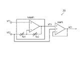
図25は、本実施形態に係る補正回路20の一例を示す回路図である。補正回路20は、第1増幅器NAMP1と、第2増幅器AMP1と、を備える。
図28は、本実施形態に係る基準電圧回路10を示す回路図である。この図28に示すように、基準電圧回路10は、第1電圧VT1と異なる温度特性を有するように、抵抗R1、R2の間の節点、すなわち、差動増幅器の非反転端子に印加される電圧を第2電圧VT2として出力してもよい。
10:基準電圧回路、
20:補正回路、
30:発振回路、
40:電圧電流変換回路、
50:周波数制御回路、
60:タイミング回路
Claims (7)
- 第1温度特性を有する第1電圧と、第1温度特性とは異なる第2温度特性を有する電圧と、の差を増幅し、第1温度特性及び第2温度特性のいずれとも異なる第3温度特性を有する第3電圧を生成する、第1増幅器であって、
第1抵抗群と、
前記第1電圧が入力される非反転端子と、前記第2温度特性を有する電圧が前記第1抵抗群を介して入力される反転端子と、非反転端子と反転端子とから入力される電圧を増幅して出力する、増幅器と、
前記増幅器の出力端子と前記増幅器の反転端子との間に接続され、前記増幅器の反転端子に対して前記第1抵抗群と対称な抵抗を有する、第2抵抗群と、
を備え、前記第1抵抗群及び前記第2抵抗群を前記増幅器の反転端子から同じ比率で分割したそれぞれの節点から、第2電圧及び前記第3電圧を出力する、第1増幅器と、
前記第2電圧及び前記第3電圧の和と、帰還電圧と、の差を増幅し、発振電圧の発振周波数を補正する第4電圧を生成する、第2増幅器と、
を有する、補正回路と、
前記第4電圧に基づいて、周波数を制御した前記発振電圧を出力する、発振回路と、
を備える、発振装置。 - 前記第1抵抗群の分割点は、前記第2温度特性を有する電圧が入力される側に接続される抵抗群が前記増幅器の反転端子に接続される抵抗群より大きくなるように設定され、
前記第2抵抗群の分割点は、前記増幅器の出力端子に接続される抵抗群が前記増幅器の反転端子に接続される抵抗群より大きくなるように設定された、
請求項1に記載の発振装置。 - 前記第2増幅器は、前記第4電圧が、前記第1電圧に対して正又は負のオフセットを有するように電圧を増幅する、
請求項1又は請求項2に記載の発振装置。 - 前記第2増幅器は、前記第4電圧が、前記第1電圧に対して正のオフセットを有するように電圧を増幅し、
前記第2電圧と前記第3電圧の和と、帰還電圧と、の差を増幅し、前記発振電圧を補正する第5電圧を生成する、第3増幅器であって、前記第5電圧が、前記第1電圧に対して負のオフセットを有するように電圧を増幅する、第3増幅器と、
前記第2増幅器の出力、及び、前記第3増幅器の出力を選択し、前記発振回路に前記第4電圧及び前記第5電圧のうちいずれかを出力する、スイッチと、
をさらに備える、請求項1又は請求項2に記載の発振装置。 - 参照電圧と、前記第1電圧と、前記第2温度特性を有する電圧とを出力する、基準電圧回路と、
前記参照電圧を参照電流に変換する、電圧電流変換回路と、
前記発振回路から出力された前記発振電圧に基づいて、タイミング信号を出力する、タイミング回路と、
前記参照電流、前記第4電圧、及び、タイミング信号に基づいて、前記発振回路に入力する電圧を出力する、周波数制御回路と、
をさらに備え、
前記発振回路は、前記周波数制御回路が出力した電圧に基づいた発振周波数を有する前記発振電圧を出力する、
請求項1から請求項4のいずれかに記載の発振装置。 - 前記第4電圧を増幅する、ゲインアンプ、
をさらに備え、
前記周波数制御回路は、前記参照電流、増幅された前記第4電圧、及び、タイミング信号に基づいて、前記発振回路に入力する電圧を出力する、
請求項5に記載の発振装置。 - 前記基準電圧回路は、前記参照電圧、前記第1電圧、及び、前記第2温度特性を有する電圧のうち少なくとも1つが可変であるように制御する、
請求項5又は請求項6に記載の発振装置。
Priority Applications (2)
| Application Number | Priority Date | Filing Date | Title |
|---|---|---|---|
| JP2019161337A JP7232156B2 (ja) | 2019-09-04 | 2019-09-04 | 発振装置 |
| US16/814,312 US10972049B2 (en) | 2019-09-04 | 2020-03-10 | Oscillation apparatus |
Applications Claiming Priority (1)
| Application Number | Priority Date | Filing Date | Title |
|---|---|---|---|
| JP2019161337A JP7232156B2 (ja) | 2019-09-04 | 2019-09-04 | 発振装置 |
Publications (2)
| Publication Number | Publication Date |
|---|---|
| JP2021040266A JP2021040266A (ja) | 2021-03-11 |
| JP7232156B2 true JP7232156B2 (ja) | 2023-03-02 |
Family
ID=74680182
Family Applications (1)
| Application Number | Title | Priority Date | Filing Date |
|---|---|---|---|
| JP2019161337A Active JP7232156B2 (ja) | 2019-09-04 | 2019-09-04 | 発振装置 |
Country Status (2)
| Country | Link |
|---|---|
| US (1) | US10972049B2 (ja) |
| JP (1) | JP7232156B2 (ja) |
Families Citing this family (1)
| Publication number | Priority date | Publication date | Assignee | Title |
|---|---|---|---|---|
| KR20240172934A (ko) * | 2023-06-02 | 2024-12-10 | 에스케이하이닉스 주식회사 | 바이어스 생성 회로 및 이를 포함하는 버퍼 회로 |
Citations (5)
| Publication number | Priority date | Publication date | Assignee | Title |
|---|---|---|---|---|
| JP2001143183A (ja) | 1999-11-15 | 2001-05-25 | Toyota Motor Corp | 入力選択出力回路および温度特性補償回路 |
| DE10155082A1 (de) | 2000-11-10 | 2002-08-29 | Denso Corp | Erfassungsvorrichtung für eine physikalische Größe mit Temperaturkompensation |
| JP2008109635A (ja) | 2006-09-25 | 2008-05-08 | Fujitsu Ltd | 温度特性補正回路及びセンサ用増幅回路 |
| JP2012138870A (ja) | 2010-12-28 | 2012-07-19 | Renesas Electronics Corp | 半導体装置 |
| JP2012154829A (ja) | 2011-01-27 | 2012-08-16 | Denso Corp | 感度温特補正回路 |
Family Cites Families (13)
| Publication number | Priority date | Publication date | Assignee | Title |
|---|---|---|---|---|
| JPS5411415B2 (ja) | 1973-05-23 | 1979-05-15 | ||
| JP4011198B2 (ja) * | 1997-06-13 | 2007-11-21 | シチズンホールディングス株式会社 | 温度補償型水晶発振器 |
| JP2001267847A (ja) * | 2000-03-17 | 2001-09-28 | Asahi Kasei Microsystems Kk | 温度補償型水晶発振器及び水晶発振器の温度補償方法 |
| JP2002300027A (ja) | 2001-03-29 | 2002-10-11 | Asahi Kasei Microsystems Kk | 発振器 |
| JP4670406B2 (ja) * | 2005-03-09 | 2011-04-13 | エプソントヨコム株式会社 | 温度補償型圧電発振器 |
| JP4991193B2 (ja) | 2006-07-04 | 2012-08-01 | 株式会社日立製作所 | 周波数可変発振器 |
| JP2010130141A (ja) | 2008-11-26 | 2010-06-10 | Epson Toyocom Corp | 電圧制御型温度補償圧電発振器 |
| JP5381162B2 (ja) * | 2009-03-03 | 2014-01-08 | セイコーエプソン株式会社 | 温度補償型発振器 |
| WO2013137867A1 (en) * | 2012-03-13 | 2013-09-19 | Intel Corporation | Temperature compensation for oscillator |
| JP6185741B2 (ja) | 2013-04-18 | 2017-08-23 | ルネサスエレクトロニクス株式会社 | 周波数同期ループ回路及び半導体集積回路 |
| KR102374841B1 (ko) * | 2015-05-28 | 2022-03-16 | 삼성전자주식회사 | 가변 전압 발생 회로 및 이를 포함하는 메모리 장치 |
| JP2018045534A (ja) * | 2016-09-15 | 2018-03-22 | 東芝メモリ株式会社 | 半導体回路 |
| JP2019118006A (ja) * | 2017-12-27 | 2019-07-18 | セイコーエプソン株式会社 | 発振回路、マイクロコンピューター、及び、電子機器 |
-
2019
- 2019-09-04 JP JP2019161337A patent/JP7232156B2/ja active Active
-
2020
- 2020-03-10 US US16/814,312 patent/US10972049B2/en active Active
Patent Citations (5)
| Publication number | Priority date | Publication date | Assignee | Title |
|---|---|---|---|---|
| JP2001143183A (ja) | 1999-11-15 | 2001-05-25 | Toyota Motor Corp | 入力選択出力回路および温度特性補償回路 |
| DE10155082A1 (de) | 2000-11-10 | 2002-08-29 | Denso Corp | Erfassungsvorrichtung für eine physikalische Größe mit Temperaturkompensation |
| JP2008109635A (ja) | 2006-09-25 | 2008-05-08 | Fujitsu Ltd | 温度特性補正回路及びセンサ用増幅回路 |
| JP2012138870A (ja) | 2010-12-28 | 2012-07-19 | Renesas Electronics Corp | 半導体装置 |
| JP2012154829A (ja) | 2011-01-27 | 2012-08-16 | Denso Corp | 感度温特補正回路 |
Also Published As
| Publication number | Publication date |
|---|---|
| JP2021040266A (ja) | 2021-03-11 |
| US20210067092A1 (en) | 2021-03-04 |
| US10972049B2 (en) | 2021-04-06 |
Similar Documents
| Publication | Publication Date | Title |
|---|---|---|
| US9285822B2 (en) | Small-circuit-scale reference voltage generating circuit | |
| US10027312B2 (en) | Low temperature coefficient clock signal generator | |
| CN111404484B (zh) | Rc振荡器及电设备 | |
| US7142042B1 (en) | Nulled error amplifier | |
| US9081404B2 (en) | Voltage regulator having input stage and current mirror | |
| US9891650B2 (en) | Current generation circuit, and bandgap reference circuit and semiconductor device including the same | |
| US6992533B2 (en) | Temperature-stabilized oscillator circuit | |
| US20080252360A1 (en) | Temperature detector circuit and oscillation frequency compensation device using the same | |
| CN102368678A (zh) | 振荡电路 | |
| US8791685B2 (en) | Bandgap reference voltage generator | |
| US20230229186A1 (en) | Bandgap reference circuit | |
| JP2012070224A (ja) | 半導体装置 | |
| JP2018120328A (ja) | 電圧生成回路 | |
| CN109194328B (zh) | 高精度片上振荡器 | |
| US6680643B2 (en) | Bandgap type reference voltage source with low supply voltage | |
| CN103792980A (zh) | 参考电压产生电路 | |
| EP3828662A1 (en) | A bandgap reference circuit, corresponding device and method | |
| CN112711288B (zh) | 具有温度变化补偿的电压参考产生 | |
| US20210349489A1 (en) | Apparatus and method for a bandgap reference | |
| US11809207B2 (en) | Temperature compensation circuit and semiconductor integrated circuit using the same | |
| US9600013B1 (en) | Bandgap reference circuit | |
| US20080074192A1 (en) | Circuit for correcting sensor temperature characteristics | |
| JP2020166648A (ja) | 基準電圧発生回路、および半導体装置 | |
| WO2024036743A1 (zh) | 电源电路与芯片 | |
| JP2021040266A (ja) | 発振装置 |
Legal Events
| Date | Code | Title | Description |
|---|---|---|---|
| A621 | Written request for application examination |
Free format text: JAPANESE INTERMEDIATE CODE: A621 Effective date: 20210820 |
|
| A977 | Report on retrieval |
Free format text: JAPANESE INTERMEDIATE CODE: A971007 Effective date: 20220725 |
|
| A131 | Notification of reasons for refusal |
Free format text: JAPANESE INTERMEDIATE CODE: A131 Effective date: 20220729 |
|
| A521 | Request for written amendment filed |
Free format text: JAPANESE INTERMEDIATE CODE: A523 Effective date: 20220927 |
|
| TRDD | Decision of grant or rejection written | ||
| A01 | Written decision to grant a patent or to grant a registration (utility model) |
Free format text: JAPANESE INTERMEDIATE CODE: A01 Effective date: 20230120 |
|
| A61 | First payment of annual fees (during grant procedure) |
Free format text: JAPANESE INTERMEDIATE CODE: A61 Effective date: 20230217 |
|
| R150 | Certificate of patent or registration of utility model |
Ref document number: 7232156 Country of ref document: JP Free format text: JAPANESE INTERMEDIATE CODE: R150 |