JP7239680B2 - 表示装置 - Google Patents
表示装置 Download PDFInfo
- Publication number
- JP7239680B2 JP7239680B2 JP2021511162A JP2021511162A JP7239680B2 JP 7239680 B2 JP7239680 B2 JP 7239680B2 JP 2021511162 A JP2021511162 A JP 2021511162A JP 2021511162 A JP2021511162 A JP 2021511162A JP 7239680 B2 JP7239680 B2 JP 7239680B2
- Authority
- JP
- Japan
- Prior art keywords
- led element
- micro led
- control switch
- micro
- light emission
- Prior art date
- Legal status (The legal status is an assumption and is not a legal conclusion. Google has not performed a legal analysis and makes no representation as to the accuracy of the status listed.)
- Active
Links
Images




Classifications
-
- G—PHYSICS
- G09—EDUCATION; CRYPTOGRAPHY; DISPLAY; ADVERTISING; SEALS
- G09G—ARRANGEMENTS OR CIRCUITS FOR CONTROL OF INDICATING DEVICES USING STATIC MEANS TO PRESENT VARIABLE INFORMATION
- G09G3/00—Control arrangements or circuits, of interest only in connection with visual indicators other than cathode-ray tubes
- G09G3/20—Control arrangements or circuits, of interest only in connection with visual indicators other than cathode-ray tubes for presentation of an assembly of a number of characters, e.g. a page, by composing the assembly by combination of individual elements arranged in a matrix no fixed position being assigned to or needed to be assigned to the individual characters or partial characters
- G09G3/22—Control arrangements or circuits, of interest only in connection with visual indicators other than cathode-ray tubes for presentation of an assembly of a number of characters, e.g. a page, by composing the assembly by combination of individual elements arranged in a matrix no fixed position being assigned to or needed to be assigned to the individual characters or partial characters using controlled light sources
- G09G3/30—Control arrangements or circuits, of interest only in connection with visual indicators other than cathode-ray tubes for presentation of an assembly of a number of characters, e.g. a page, by composing the assembly by combination of individual elements arranged in a matrix no fixed position being assigned to or needed to be assigned to the individual characters or partial characters using controlled light sources using electroluminescent panels
- G09G3/32—Control arrangements or circuits, of interest only in connection with visual indicators other than cathode-ray tubes for presentation of an assembly of a number of characters, e.g. a page, by composing the assembly by combination of individual elements arranged in a matrix no fixed position being assigned to or needed to be assigned to the individual characters or partial characters using controlled light sources using electroluminescent panels semiconductive, e.g. using light-emitting diodes [LED]
-
- G—PHYSICS
- G09—EDUCATION; CRYPTOGRAPHY; DISPLAY; ADVERTISING; SEALS
- G09G—ARRANGEMENTS OR CIRCUITS FOR CONTROL OF INDICATING DEVICES USING STATIC MEANS TO PRESENT VARIABLE INFORMATION
- G09G2300/00—Aspects of the constitution of display devices
- G09G2300/02—Composition of display devices
- G09G2300/026—Video wall, i.e. juxtaposition of a plurality of screens to create a display screen of bigger dimensions
-
- G—PHYSICS
- G09—EDUCATION; CRYPTOGRAPHY; DISPLAY; ADVERTISING; SEALS
- G09G—ARRANGEMENTS OR CIRCUITS FOR CONTROL OF INDICATING DEVICES USING STATIC MEANS TO PRESENT VARIABLE INFORMATION
- G09G2300/00—Aspects of the constitution of display devices
- G09G2300/04—Structural and physical details of display devices
- G09G2300/0439—Pixel structures
- G09G2300/0452—Details of colour pixel setup, e.g. pixel composed of a red, a blue and two green components
-
- G—PHYSICS
- G09—EDUCATION; CRYPTOGRAPHY; DISPLAY; ADVERTISING; SEALS
- G09G—ARRANGEMENTS OR CIRCUITS FOR CONTROL OF INDICATING DEVICES USING STATIC MEANS TO PRESENT VARIABLE INFORMATION
- G09G2300/00—Aspects of the constitution of display devices
- G09G2300/08—Active matrix structure, i.e. with use of active elements, inclusive of non-linear two terminal elements, in the pixels together with light emitting or modulating elements
- G09G2300/0809—Several active elements per pixel in active matrix panels
- G09G2300/0842—Several active elements per pixel in active matrix panels forming a memory circuit, e.g. a dynamic memory with one capacitor
-
- G—PHYSICS
- G09—EDUCATION; CRYPTOGRAPHY; DISPLAY; ADVERTISING; SEALS
- G09G—ARRANGEMENTS OR CIRCUITS FOR CONTROL OF INDICATING DEVICES USING STATIC MEANS TO PRESENT VARIABLE INFORMATION
- G09G2300/00—Aspects of the constitution of display devices
- G09G2300/08—Active matrix structure, i.e. with use of active elements, inclusive of non-linear two terminal elements, in the pixels together with light emitting or modulating elements
- G09G2300/0809—Several active elements per pixel in active matrix panels
- G09G2300/0842—Several active elements per pixel in active matrix panels forming a memory circuit, e.g. a dynamic memory with one capacitor
- G09G2300/0861—Several active elements per pixel in active matrix panels forming a memory circuit, e.g. a dynamic memory with one capacitor with additional control of the display period without amending the charge stored in a pixel memory, e.g. by means of additional select electrodes
-
- G—PHYSICS
- G09—EDUCATION; CRYPTOGRAPHY; DISPLAY; ADVERTISING; SEALS
- G09G—ARRANGEMENTS OR CIRCUITS FOR CONTROL OF INDICATING DEVICES USING STATIC MEANS TO PRESENT VARIABLE INFORMATION
- G09G2310/00—Command of the display device
- G09G2310/08—Details of timing specific for flat panels, other than clock recovery
-
- G—PHYSICS
- G09—EDUCATION; CRYPTOGRAPHY; DISPLAY; ADVERTISING; SEALS
- G09G—ARRANGEMENTS OR CIRCUITS FOR CONTROL OF INDICATING DEVICES USING STATIC MEANS TO PRESENT VARIABLE INFORMATION
- G09G2320/00—Control of display operating conditions
- G09G2320/02—Improving the quality of display appearance
- G09G2320/0233—Improving the luminance or brightness uniformity across the screen
-
- G—PHYSICS
- G09—EDUCATION; CRYPTOGRAPHY; DISPLAY; ADVERTISING; SEALS
- G09G—ARRANGEMENTS OR CIRCUITS FOR CONTROL OF INDICATING DEVICES USING STATIC MEANS TO PRESENT VARIABLE INFORMATION
- G09G2320/00—Control of display operating conditions
- G09G2320/02—Improving the quality of display appearance
- G09G2320/0242—Compensation of deficiencies in the appearance of colours
-
- H—ELECTRICITY
- H10—SEMICONDUCTOR DEVICES; ELECTRIC SOLID-STATE DEVICES NOT OTHERWISE PROVIDED FOR
- H10W—GENERIC PACKAGES, INTERCONNECTIONS, CONNECTORS OR OTHER CONSTRUCTIONAL DETAILS OF DEVICES COVERED BY CLASS H10
- H10W90/00—Package configurations
Landscapes
- Engineering & Computer Science (AREA)
- Physics & Mathematics (AREA)
- Computer Hardware Design (AREA)
- General Physics & Mathematics (AREA)
- Theoretical Computer Science (AREA)
- Control Of Indicators Other Than Cathode Ray Tubes (AREA)
- Control Of El Displays (AREA)
- Led Devices (AREA)
- Devices For Indicating Variable Information By Combining Individual Elements (AREA)
Description
1a 配置面
1b 反対面
1s 側面
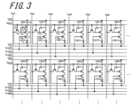
6 駆動部
13a 第1電流制御スイッチ
13b 第2電流制御スイッチ
13c 第3電流制御スイッチ
14a 第1マイクロLED素子
14b 第2マイクロLED素子
14R 第1マイクロLED素子としての赤色マイクロLED素子
14G 第2マイクロLED素子としての緑色マイクロLED素子
14B 第3マイクロLED素子としての青色マイクロLED素子
15a 第1画素部
15b 第2画素部
15R 第1画素部
15G 第2画素部
15B 第3画素部
16k1 第1駆動線
16k2 第2駆動線
16k3 第3駆動線
19a 第1期間制御スイッチ
19b 第2期間制御スイッチ
19c 第3期間制御スイッチ
30 側面配線
50 発光制御部
Claims (4)
- 赤色光を発光する第1マイクロLED素子を含む第1画素部と、緑色光を発光する第2マイクロLED素子を含む第2画素部と、青色光を発光する第3マイクロLED素子を含む第3画素部と、が基板上に配置されており、
前記第1マイクロLED素子と前記第2マイクロLED素子と前記第3マイクロLED素子とのそれぞれの発光強度を制御する発光制御部を備える表示装置であって、
前記第1画素部は、前記第1マイクロLED素子に供給される第1駆動電流を制御する第1電流制御スイッチと、前記第1マイクロLED素子の第1発光期間を制御する第1期間制御スイッチと、を含んでおり、
前記第2画素部は、前記第2マイクロLED素子に供給される第2駆動電流を制御する第2電流制御スイッチと、前記第2マイクロLED素子の第2発光期間を制御する第2期間制御スイッチと、を含んでおり、
前記第3画素部は、前記第3マイクロLED素子に供給される第3駆動電流を制御する第3電流制御スイッチと、前記第3マイクロLED素子の第3発光期間を制御する第3期間制御スイッチと、を含んでおり、
前記第1電流制御スイッチと前記第1期間制御スイッチと前記第2電流制御スイッチと前記第2期間制御スイッチと前記第3電流制御スイッチと前記第3期間制御スイッチとは、前記発光制御部に接続されており、
前記発光制御部は、前記第1発光期間と前記第2発光期間と前記第3発光期間とが重なることによって、カラーの階調表示を可能とするとともに、前記第3マイクロLED素子、前記第1マイクロLED素子、前記第2マイクロLED素子の順に早く発光させる制御を行い、さらに、前記第1駆動電流と前記第2駆動電流と前記第3駆動電流とは、それぞれが漸次または段階的に大きくなるとともに、前記第3駆動電流の増加率が前記第1駆動電流の増加率よりも大きく、かつ前記第1駆動電流の増加率が前記第2駆動電流の増加率よりも大きくなる制御を行う表示装置。 - 前記第1期間制御スイッチは、前記第1電流制御スイッチと前記第1マイクロLED素子を接続する第1駆動線上に配置されており、
前記第2期間制御スイッチは、前記第2電流制御スイッチと前記第2マイクロLED素子を接続する第2駆動線上に配置されており、
前記第3期間制御スイッチは、前記第3電流制御スイッチと前記第3マイクロLED素子を接続する第3駆動線上に配置されている請求項1に記載の表示装置。 - 前記第1マイクロLED素子と前記第2マイクロLED素子と前記第3マイクロLED素子とは、それぞれ発光効率が異なるとともに、発光効率が低い方から順に前記第1マイクロLED素子、前記第2マイクロLED素子、前記第3マイクロLED素子であり、
前記発光制御部は、前記第1駆動電流の前記第1発光期間での積分値をS1とし、前記第2駆動電流の前記第2発光期間での積分値をS2とし、前記第3駆動電流の前記第3発光期間での積分値をS3としたとき、S1>S2>S3となる制御を行う請求項1または2に記載の表示装置。 - 前記基板は、前記第1画素部と前記第2画素部と前記第3画素部とが配置される配置面と、前記配置面と反対側の反対面と、側面と、を有しており、
前記側面に側面配線が配置されているとともに前記反対面の側に前記発光制御部を含む駆動部が配置されており、
前記第1マイクロLED素子と前記第2マイクロLED素子と前記第3マイクロLED素子とは、前記側面配線を介して前記駆動部に接続されている請求項1乃至請求項3のいずれか1項に記載の表示装置。
Applications Claiming Priority (3)
| Application Number | Priority Date | Filing Date | Title |
|---|---|---|---|
| JP2019065770 | 2019-03-29 | ||
| JP2019065770 | 2019-03-29 | ||
| PCT/JP2020/003874 WO2020202766A1 (ja) | 2019-03-29 | 2020-02-03 | 表示装置 |
Publications (2)
| Publication Number | Publication Date |
|---|---|
| JPWO2020202766A1 JPWO2020202766A1 (ja) | 2020-10-08 |
| JP7239680B2 true JP7239680B2 (ja) | 2023-03-14 |
Family
ID=72667878
Family Applications (1)
| Application Number | Title | Priority Date | Filing Date |
|---|---|---|---|
| JP2021511162A Active JP7239680B2 (ja) | 2019-03-29 | 2020-02-03 | 表示装置 |
Country Status (5)
| Country | Link |
|---|---|
| US (1) | US11631367B2 (ja) |
| EP (2) | EP4113494A1 (ja) |
| JP (1) | JP7239680B2 (ja) |
| CN (1) | CN113614823A (ja) |
| WO (1) | WO2020202766A1 (ja) |
Cited By (1)
| Publication number | Priority date | Publication date | Assignee | Title |
|---|---|---|---|---|
| KR102949365B1 (ko) * | 2023-09-27 | 2026-04-20 | 모아컴코리아주식회사 | 화질 향상이 가능한 표시 장치 |
Families Citing this family (11)
| Publication number | Priority date | Publication date | Assignee | Title |
|---|---|---|---|---|
| JP7239680B2 (ja) | 2019-03-29 | 2023-03-14 | 京セラ株式会社 | 表示装置 |
| CN111682044B (zh) * | 2020-07-10 | 2022-04-08 | 深圳市华星光电半导体显示技术有限公司 | 一种显示面板及其制备方法、显示装置 |
| WO2022150843A1 (en) * | 2021-01-08 | 2022-07-14 | Magic Leap, Inc. | Single pupil rgb light source |
| CN115315742B (zh) * | 2021-03-04 | 2025-04-11 | 京东方科技集团股份有限公司 | 发光基板、显示装置和驱动发光基板的方法 |
| CN117321672A (zh) * | 2021-05-26 | 2023-12-29 | 京瓷株式会社 | 像素电路、显示面板、显示装置以及复合型显示装置 |
| JP2022191068A (ja) | 2021-06-15 | 2022-12-27 | 株式会社ジャパンディスプレイ | 表示装置 |
| JP7746758B2 (ja) * | 2021-09-17 | 2025-10-01 | 沖電気工業株式会社 | 半導体装置 |
| DE112023001774T5 (de) | 2022-03-31 | 2025-06-18 | Nichia Corporation | Lichtemittierende vorrichtung und verfahren zum ansteuern einer lichtemittierenden vorrichtung |
| TW202433445A (zh) * | 2023-02-03 | 2024-08-16 | 加拿大商弗瑞爾公司 | 透明顯示器 |
| WO2025095940A1 (en) | 2023-10-31 | 2025-05-08 | Google Llc | Optimized pixel performance in a display system |
| KR20250149851A (ko) * | 2024-04-09 | 2025-10-17 | 삼성디스플레이 주식회사 | 표시 장치 및 그의 구동 방법 |
Citations (2)
| Publication number | Priority date | Publication date | Assignee | Title |
|---|---|---|---|---|
| JP2018519539A (ja) | 2015-06-05 | 2018-07-19 | アップル インコーポレイテッド | 表示パネル用の発光制御装置及び方法 |
| US20190006335A1 (en) | 2017-06-30 | 2019-01-03 | Lg Display Co., Ltd. | Display device and method for fabricating the same |
Family Cites Families (15)
| Publication number | Priority date | Publication date | Assignee | Title |
|---|---|---|---|---|
| GB0227356D0 (en) | 2002-11-23 | 2002-12-31 | Koninkl Philips Electronics Nv | Colour active matrix electroluminescent display devices |
| JP4804711B2 (ja) * | 2003-11-21 | 2011-11-02 | 株式会社 日立ディスプレイズ | 画像表示装置 |
| JP4437110B2 (ja) * | 2004-11-17 | 2010-03-24 | 三星モバイルディスプレイ株式會社 | 有機発光表示装置,有機発光表示装置の駆動方法及び画素回路の駆動方法 |
| JP2007203602A (ja) | 2006-02-02 | 2007-08-16 | Seiko Epson Corp | 発光装置、電子機器および画像処理装置 |
| KR101058104B1 (ko) | 2009-01-29 | 2011-08-24 | 삼성모바일디스플레이주식회사 | 적어도 2종의 유기 전계 발광 소자들을 구비하는 조명 장치및 이의 구동 방법 |
| JP5338605B2 (ja) | 2009-10-02 | 2013-11-13 | ソニー株式会社 | 自発光素子パネル、画像表示装置、および、自発光素子のパッシブ駆動方法 |
| JP2012022181A (ja) | 2010-07-15 | 2012-02-02 | Canon Inc | 発光装置 |
| US9600123B2 (en) * | 2012-10-18 | 2017-03-21 | Sharp Kabushiki Kaisha | Optical sensor and electronic apparatus |
| KR20150112108A (ko) * | 2014-03-26 | 2015-10-07 | 삼성디스플레이 주식회사 | 표시 장치 |
| CN106297672B (zh) * | 2016-10-28 | 2017-08-29 | 京东方科技集团股份有限公司 | 像素驱动电路、驱动方法和显示设备 |
| KR102687577B1 (ko) * | 2016-12-30 | 2024-07-22 | 엘지디스플레이 주식회사 | 발광 다이오드 표시 장치 및 이를 이용한 멀티 스크린 표시 장치 |
| JP6856472B2 (ja) * | 2017-07-31 | 2021-04-07 | 京セラ株式会社 | 表示装置 |
| KR102394683B1 (ko) * | 2018-03-06 | 2022-05-09 | 삼성디스플레이 주식회사 | 펜타일 픽셀 구조를 가지는 유기 발광 표시 장치의 표시 패널 |
| CN108364972B (zh) * | 2018-04-03 | 2024-05-31 | 中山大学 | 柔性薄膜GaN基纳米柱LED阵列微显示器件及其制作方法 |
| JP7239680B2 (ja) | 2019-03-29 | 2023-03-14 | 京セラ株式会社 | 表示装置 |
-
2020
- 2020-02-03 JP JP2021511162A patent/JP7239680B2/ja active Active
- 2020-02-03 EP EP22191630.7A patent/EP4113494A1/en not_active Withdrawn
- 2020-02-03 WO PCT/JP2020/003874 patent/WO2020202766A1/ja not_active Ceased
- 2020-02-03 EP EP20784073.7A patent/EP3951760A4/en not_active Withdrawn
- 2020-02-03 CN CN202080022640.6A patent/CN113614823A/zh active Pending
- 2020-02-03 US US17/598,732 patent/US11631367B2/en active Active
Patent Citations (2)
| Publication number | Priority date | Publication date | Assignee | Title |
|---|---|---|---|---|
| JP2018519539A (ja) | 2015-06-05 | 2018-07-19 | アップル インコーポレイテッド | 表示パネル用の発光制御装置及び方法 |
| US20190006335A1 (en) | 2017-06-30 | 2019-01-03 | Lg Display Co., Ltd. | Display device and method for fabricating the same |
Cited By (1)
| Publication number | Priority date | Publication date | Assignee | Title |
|---|---|---|---|---|
| KR102949365B1 (ko) * | 2023-09-27 | 2026-04-20 | 모아컴코리아주식회사 | 화질 향상이 가능한 표시 장치 |
Also Published As
| Publication number | Publication date |
|---|---|
| CN113614823A (zh) | 2021-11-05 |
| EP3951760A1 (en) | 2022-02-09 |
| US11631367B2 (en) | 2023-04-18 |
| WO2020202766A1 (ja) | 2020-10-08 |
| EP4113494A1 (en) | 2023-01-04 |
| EP3951760A4 (en) | 2022-11-09 |
| US20220157230A1 (en) | 2022-05-19 |
| JPWO2020202766A1 (ja) | 2020-10-08 |
Similar Documents
| Publication | Publication Date | Title |
|---|---|---|
| JP7239680B2 (ja) | 表示装置 | |
| CN112750397B (zh) | 显示面板及其驱动方法、显示装置 | |
| TWI820083B (zh) | 顯示面板以及顯示面板的驅動方法 | |
| CN108133688B (zh) | 电致发光显示装置 | |
| TWI352948B (en) | Light emitting display and method of driving there | |
| KR102049955B1 (ko) | 스마트 픽셀 조명 및 디스플레이 마이크로컨트롤러 | |
| CN107644889B (zh) | 显示面板和包括该显示面板的显示装置 | |
| US9466244B2 (en) | EL display device and production method therefor | |
| US20060123293A1 (en) | Organic light emitting display | |
| CN110473978A (zh) | 有机发光显示设备 | |
| TW202004722A (zh) | 顯示面板 | |
| KR102748791B1 (ko) | 디스플레이 모듈 및 디스플레이 모듈의 구동 방법 | |
| CN102354479B (zh) | 电致发光显示器及其驱动方法 | |
| CN110556075B (zh) | 显示装置以及控制该显示装置的方法 | |
| CN116613184A (zh) | Led显示面板 | |
| CN107785392A (zh) | 显示装置 | |
| CN101093640B (zh) | 双扫描显示装置 | |
| US12555525B2 (en) | Driver circuit for light emitting modules with combined active and passive matrix functionalities | |
| WO2023063164A1 (ja) | 表示装置 | |
| WO2022109845A1 (en) | Method for image display in a display apparatus, display apparatus, peripheral sensing circuit, and pixel driving circuit | |
| JP7362742B2 (ja) | 表示装置 | |
| KR102524142B1 (ko) | 데이터 구동부 및 그것을 포함하는 표시 장치 | |
| KR100459166B1 (ko) | 전류구동 표시소자의 구동 회로 | |
| JP2003108033A (ja) | 表示装置 | |
| US12315858B2 (en) | Display device |
Legal Events
| Date | Code | Title | Description |
|---|---|---|---|
| A621 | Written request for application examination |
Free format text: JAPANESE INTERMEDIATE CODE: A621 Effective date: 20210906 |
|
| A131 | Notification of reasons for refusal |
Free format text: JAPANESE INTERMEDIATE CODE: A131 Effective date: 20220510 |
|
| A521 | Request for written amendment filed |
Free format text: JAPANESE INTERMEDIATE CODE: A523 Effective date: 20220620 |
|
| A131 | Notification of reasons for refusal |
Free format text: JAPANESE INTERMEDIATE CODE: A131 Effective date: 20220802 |
|
| A521 | Request for written amendment filed |
Free format text: JAPANESE INTERMEDIATE CODE: A523 Effective date: 20221003 |
|
| A02 | Decision of refusal |
Free format text: JAPANESE INTERMEDIATE CODE: A02 Effective date: 20221025 |
|
| A521 | Request for written amendment filed |
Free format text: JAPANESE INTERMEDIATE CODE: A523 Effective date: 20230106 |
|
| C60 | Trial request (containing other claim documents, opposition documents) |
Free format text: JAPANESE INTERMEDIATE CODE: C60 Effective date: 20230106 |
|
| A911 | Transfer to examiner for re-examination before appeal (zenchi) |
Free format text: JAPANESE INTERMEDIATE CODE: A911 Effective date: 20230117 |
|
| C21 | Notice of transfer of a case for reconsideration by examiners before appeal proceedings |
Free format text: JAPANESE INTERMEDIATE CODE: C21 Effective date: 20230124 |
|
| TRDD | Decision of grant or rejection written | ||
| A01 | Written decision to grant a patent or to grant a registration (utility model) |
Free format text: JAPANESE INTERMEDIATE CODE: A01 Effective date: 20230214 |
|
| A61 | First payment of annual fees (during grant procedure) |
Free format text: JAPANESE INTERMEDIATE CODE: A61 Effective date: 20230302 |
|
| R150 | Certificate of patent or registration of utility model |
Ref document number: 7239680 Country of ref document: JP Free format text: JAPANESE INTERMEDIATE CODE: R150 |