JP7269802B2 - サーマルプリントヘッドおよびその製造方法 - Google Patents
サーマルプリントヘッドおよびその製造方法 Download PDFInfo
- Publication number
- JP7269802B2 JP7269802B2 JP2019117056A JP2019117056A JP7269802B2 JP 7269802 B2 JP7269802 B2 JP 7269802B2 JP 2019117056 A JP2019117056 A JP 2019117056A JP 2019117056 A JP2019117056 A JP 2019117056A JP 7269802 B2 JP7269802 B2 JP 7269802B2
- Authority
- JP
- Japan
- Prior art keywords
- scanning direction
- main surface
- convex portion
- top surface
- pair
- Prior art date
- Legal status (The legal status is an assumption and is not a legal conclusion. Google has not performed a legal analysis and makes no representation as to the accuracy of the status listed.)
- Active
Links
Images










Classifications
-
- B—PERFORMING OPERATIONS; TRANSPORTING
- B41—PRINTING; LINING MACHINES; TYPEWRITERS; STAMPS
- B41J—TYPEWRITERS; SELECTIVE PRINTING MECHANISMS, i.e. MECHANISMS PRINTING OTHERWISE THAN FROM A FORME; CORRECTION OF TYPOGRAPHICAL ERRORS
- B41J2/00—Typewriters or selective printing mechanisms characterised by the printing or marking process for which they are designed
- B41J2/315—Typewriters or selective printing mechanisms characterised by the printing or marking process for which they are designed characterised by selective application of heat to a heat sensitive printing or impression-transfer material
- B41J2/32—Typewriters or selective printing mechanisms characterised by the printing or marking process for which they are designed characterised by selective application of heat to a heat sensitive printing or impression-transfer material using thermal heads
- B41J2/335—Structure of thermal heads
- B41J2/34—Structure of thermal heads comprising semiconductors
-
- B—PERFORMING OPERATIONS; TRANSPORTING
- B41—PRINTING; LINING MACHINES; TYPEWRITERS; STAMPS
- B41J—TYPEWRITERS; SELECTIVE PRINTING MECHANISMS, i.e. MECHANISMS PRINTING OTHERWISE THAN FROM A FORME; CORRECTION OF TYPOGRAPHICAL ERRORS
- B41J2/00—Typewriters or selective printing mechanisms characterised by the printing or marking process for which they are designed
- B41J2/315—Typewriters or selective printing mechanisms characterised by the printing or marking process for which they are designed characterised by selective application of heat to a heat sensitive printing or impression-transfer material
- B41J2/32—Typewriters or selective printing mechanisms characterised by the printing or marking process for which they are designed characterised by selective application of heat to a heat sensitive printing or impression-transfer material using thermal heads
- B41J2/335—Structure of thermal heads
- B41J2/33505—Constructional details
-
- B—PERFORMING OPERATIONS; TRANSPORTING
- B41—PRINTING; LINING MACHINES; TYPEWRITERS; STAMPS
- B41J—TYPEWRITERS; SELECTIVE PRINTING MECHANISMS, i.e. MECHANISMS PRINTING OTHERWISE THAN FROM A FORME; CORRECTION OF TYPOGRAPHICAL ERRORS
- B41J2/00—Typewriters or selective printing mechanisms characterised by the printing or marking process for which they are designed
- B41J2/315—Typewriters or selective printing mechanisms characterised by the printing or marking process for which they are designed characterised by selective application of heat to a heat sensitive printing or impression-transfer material
- B41J2/32—Typewriters or selective printing mechanisms characterised by the printing or marking process for which they are designed characterised by selective application of heat to a heat sensitive printing or impression-transfer material using thermal heads
- B41J2/335—Structure of thermal heads
- B41J2/3355—Structure of thermal heads characterised by materials
-
- B—PERFORMING OPERATIONS; TRANSPORTING
- B41—PRINTING; LINING MACHINES; TYPEWRITERS; STAMPS
- B41J—TYPEWRITERS; SELECTIVE PRINTING MECHANISMS, i.e. MECHANISMS PRINTING OTHERWISE THAN FROM A FORME; CORRECTION OF TYPOGRAPHICAL ERRORS
- B41J2/00—Typewriters or selective printing mechanisms characterised by the printing or marking process for which they are designed
- B41J2/315—Typewriters or selective printing mechanisms characterised by the printing or marking process for which they are designed characterised by selective application of heat to a heat sensitive printing or impression-transfer material
- B41J2/32—Typewriters or selective printing mechanisms characterised by the printing or marking process for which they are designed characterised by selective application of heat to a heat sensitive printing or impression-transfer material using thermal heads
- B41J2/335—Structure of thermal heads
- B41J2/3359—Manufacturing processes
Landscapes
- Engineering & Computer Science (AREA)
- Manufacturing & Machinery (AREA)
- Electronic Switches (AREA)
Description
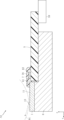
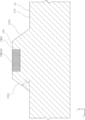
1 :ヘッド基板
1A :材料基板
2 :保護層
3 :電極層
3A :導電膜
4 :抵抗体層
4A :抵抗体膜
5 :接続基板
7 :ドライバIC
8 :放熱部材
11 :主面
11A :主面
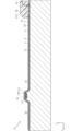
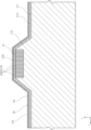
13 :凸部
13A :凸部中間体
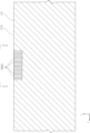
15 :蓄熱部
19 :絶縁層
21 :パッド用開口
31 :個別電極層
32 :共通電極層
41 :発熱部
59 :コネクタ
61 :ワイヤ
62 :ワイヤ
78 :保護樹脂
91 :プラテンローラ
130 :頂面
130A :頂面
131 :第1傾斜外面
131A :傾斜外面
132 :第2傾斜外面
150 :微小柱状蓄熱部材
150A :柱状微小細孔
311 ;電極パッド部
323 :共通部
324 :櫛歯部
325 :延長部
x :主走査方向
y :副走査方向
α1、α2:角度
Claims (2)
- 主面を有する基板と、上記基板の上記主面上に形成され、主走査方向に延びる凸部と、上記凸部の頂面に主走査方向に配列された複数の発熱部と、を含み、上記凸部には、その頂面に上端が位置し、上記凸部の深さ方向に所定長さで延びる多数の微小柱状蓄熱部材を、副走査方向所定幅で主走査方向に所定長さ延びる所定領域に埋設形成することにより、蓄熱部が形成されており、上記凸部は、上記頂面と、当該頂面に対して副走査方向両側につながり、かつ当該頂面から副走査方向に離れるにしたがって低位となるように上記主面に対して傾斜する一対の第1傾斜外面とを含む、サーマルプリントヘッドの製造方法であって、
主面を有する単結晶半導体からなる材料基板の上記主面における上記凸部の上記頂面となるべき領域に上記多数の微小柱状蓄熱部材を埋設配置した後、
上記材料基板の上記主面に対して異方性エッチングを行うことにより、上記一対の傾斜外面と上記頂面とを有する上記凸部を形成するに際し、
上記多数の微小柱状蓄熱部材は、Siウエハからなる上記材料基板の上記主面に深掘りエッチングにより上記材料基板の厚み方向に延びる多数の微小細孔を形成し、熱酸化処理を行うことにより上記多数の微小細孔をSiO2に変化させることにより形成し、
上記一対の第1傾斜外面は、上記材料基板の(100)面である上記主面に対し、上記材料基板の上記主面のうち、上記多数の微小蓄熱部材が埋設形成された領域をマスクとして異方性エッチングを行うことにより形成することを特徴とする、サーマルプリントヘッドの製造方法。 - 主面を有する基板と、上記基板の上記主面上に形成され、主走査方向に延びる凸部と、上記凸部の頂面に主走査方向に配列された複数の発熱部と、を含み、上記凸部には、その頂面に上端が位置し、上記凸部の深さ方向に所定長さで延びる多数の微小柱状蓄熱部材を、副走査方向所定幅で主走査方向に所定長さ延びる所定領域に埋設形成することにより、蓄熱部が形成されており、上記凸部は、上記頂面と、当該頂面に対して副走査方向両側につながり、かつ当該頂面から副走査方向に離れるにしたがって低位となるように上記主面に対して傾斜する一対の第2傾斜外面と、上記一対の第2傾斜外面に対して上記頂面とは副走査方向の反対側につながり、かつ当該頂面から副走査方向に離れるにしたがって低位となるように、上記主面に対して上記一対の第2傾斜外面よりも大きな角度で傾斜する一対の第1傾斜外面とを含みを含む、サーマルプリントヘッドの製造方法であって、
主面を有する単結晶半導体からなる材料基板の上記主面における上記凸部の上記頂面となるべき領域に上記多数の微小柱状蓄熱部材を埋設配置した後、
上記材料基板の上記主面に対して異方性エッチングを行うことにより、上記一対の第1傾斜外面と、上記第2傾斜外面と、上記頂面とを有する上記凸部を形成するに際し、
上記多数の微小柱状蓄熱部材は、Siウエハからなる上記材料基板の上記主面に深掘りエッチングにより上記材料基板の厚み方向に延びる多数の微小細孔を形成し、熱酸化処理を行うことにより上記多数の微小細孔をSiO2に変化させることにより形成し、
上記一対の第1傾斜外面および上記一対の第2傾斜外面は、上記材料基板の(100)面である上記主面に対して異方性エッチングを行うことにより上記一対の第1傾斜外面となるべき一対の傾斜外面を形成した後、上記材料基板の上記主面のうち、上記多数の微小蓄熱部材が埋設形成された領域をマスクとして追加の異方性エッチングを行うことにより、上記一対の第2傾斜外面を形成することを特徴とする、サーマルプリントヘッドの製造方法。
Priority Applications (2)
| Application Number | Priority Date | Filing Date | Title |
|---|---|---|---|
| JP2019117056A JP7269802B2 (ja) | 2019-06-25 | 2019-06-25 | サーマルプリントヘッドおよびその製造方法 |
| US16/908,143 US11279145B2 (en) | 2019-06-25 | 2020-06-22 | Thermal print head and method of manufacturing the same |
Applications Claiming Priority (1)
| Application Number | Priority Date | Filing Date | Title |
|---|---|---|---|
| JP2019117056A JP7269802B2 (ja) | 2019-06-25 | 2019-06-25 | サーマルプリントヘッドおよびその製造方法 |
Publications (2)
| Publication Number | Publication Date |
|---|---|
| JP2021003809A JP2021003809A (ja) | 2021-01-14 |
| JP7269802B2 true JP7269802B2 (ja) | 2023-05-09 |
Family
ID=74044377
Family Applications (1)
| Application Number | Title | Priority Date | Filing Date |
|---|---|---|---|
| JP2019117056A Active JP7269802B2 (ja) | 2019-06-25 | 2019-06-25 | サーマルプリントヘッドおよびその製造方法 |
Country Status (2)
| Country | Link |
|---|---|
| US (1) | US11279145B2 (ja) |
| JP (1) | JP7269802B2 (ja) |
Families Citing this family (2)
| Publication number | Priority date | Publication date | Assignee | Title |
|---|---|---|---|---|
| JP7715553B2 (ja) * | 2021-07-08 | 2025-07-30 | ローム株式会社 | サーマルプリントヘッドの製造方法 |
| JP7803701B2 (ja) * | 2021-12-02 | 2026-01-21 | ローム株式会社 | サーマルプリントヘッド、および、サーマルプリントヘッドの製造方法 |
Citations (6)
| Publication number | Priority date | Publication date | Assignee | Title |
|---|---|---|---|---|
| JP2003165241A (ja) | 2001-12-03 | 2003-06-10 | Alps Electric Co Ltd | サーマルヘッド |
| JP2004303744A (ja) | 2003-03-28 | 2004-10-28 | Denso Corp | モノリシックマイクロ波集積回路およびその製造方法 |
| JP2004342774A (ja) | 2003-05-14 | 2004-12-02 | Fuji Electric Device Technology Co Ltd | 半導体装置の製造方法 |
| US20070042606A1 (en) | 2005-08-19 | 2007-02-22 | Honeywell International Inc. | Creating novel structures using deep trenching of oriented silicon substrates |
| JP2014231216A (ja) | 2012-08-29 | 2014-12-11 | ローム株式会社 | サーマルプリントヘッドおよびサーマルプリンタ |
| JP2019014233A (ja) | 2017-06-08 | 2019-01-31 | ローム株式会社 | サーマルプリントヘッド |
Family Cites Families (5)
| Publication number | Priority date | Publication date | Assignee | Title |
|---|---|---|---|---|
| JPS6295239A (ja) | 1985-10-23 | 1987-05-01 | Alps Electric Co Ltd | サ−マルヘツド |
| EP1226951A3 (en) | 2001-01-29 | 2003-03-12 | Alps Electric Co., Ltd. | Power-saving thermal head |
| US6767081B2 (en) * | 2001-12-03 | 2004-07-27 | Alps Electric Co., Ltd. | Thermal head |
| JP2007269036A (ja) | 2007-06-04 | 2007-10-18 | Rohm Co Ltd | 薄膜型サーマルプリントヘッドの発熱体抵抗値の調整方法 |
| JP6650264B2 (ja) * | 2015-12-25 | 2020-02-19 | ローム株式会社 | サーマルプリントヘッド |
-
2019
- 2019-06-25 JP JP2019117056A patent/JP7269802B2/ja active Active
-
2020
- 2020-06-22 US US16/908,143 patent/US11279145B2/en active Active
Patent Citations (6)
| Publication number | Priority date | Publication date | Assignee | Title |
|---|---|---|---|---|
| JP2003165241A (ja) | 2001-12-03 | 2003-06-10 | Alps Electric Co Ltd | サーマルヘッド |
| JP2004303744A (ja) | 2003-03-28 | 2004-10-28 | Denso Corp | モノリシックマイクロ波集積回路およびその製造方法 |
| JP2004342774A (ja) | 2003-05-14 | 2004-12-02 | Fuji Electric Device Technology Co Ltd | 半導体装置の製造方法 |
| US20070042606A1 (en) | 2005-08-19 | 2007-02-22 | Honeywell International Inc. | Creating novel structures using deep trenching of oriented silicon substrates |
| JP2014231216A (ja) | 2012-08-29 | 2014-12-11 | ローム株式会社 | サーマルプリントヘッドおよびサーマルプリンタ |
| JP2019014233A (ja) | 2017-06-08 | 2019-01-31 | ローム株式会社 | サーマルプリントヘッド |
Also Published As
| Publication number | Publication date |
|---|---|
| US11279145B2 (en) | 2022-03-22 |
| US20200406631A1 (en) | 2020-12-31 |
| JP2021003809A (ja) | 2021-01-14 |
Similar Documents
| Publication | Publication Date | Title |
|---|---|---|
| JP6371529B2 (ja) | サーマルプリントヘッド、サーマルプリンタ | |
| JP7269802B2 (ja) | サーマルプリントヘッドおよびその製造方法 | |
| JP7413066B2 (ja) | サーマルプリントヘッドの製造方法、サーマルプリントヘッドおよびサーマルプリンタ | |
| JP7545858B2 (ja) | サーマルプリントヘッド、および、サーマルプリントヘッドの製造方法 | |
| JP6209019B2 (ja) | サーマルプリントヘッド、サーマルプリンタ | |
| JP7284640B2 (ja) | サーマルプリントヘッド | |
| JP7297564B2 (ja) | サーマルプリントヘッドおよびその製造方法 | |
| WO2021149617A1 (ja) | サーマルプリントヘッドおよびサーマルプリントヘッドの製造方法 | |
| JP7151054B2 (ja) | サーマルプリントヘッド、および、その製造方法 | |
| JP7219634B2 (ja) | サーマルプリントヘッド | |
| JP5802032B2 (ja) | サーマルプリントヘッド | |
| JP6557066B2 (ja) | サーマルプリントヘッドの製造方法およびサーマルプリントヘッド | |
| JP6786669B2 (ja) | サーマルプリントヘッド、サーマルプリンタ | |
| CN115339245A (zh) | 热敏打印头及热敏打印头的制造方法 | |
| JP7803701B2 (ja) | サーマルプリントヘッド、および、サーマルプリントヘッドの製造方法 | |
| JP5670076B2 (ja) | サーマルプリントヘッドおよびその製造方法 | |
| JP7557320B2 (ja) | サーマルプリントヘッド | |
| JP6341723B2 (ja) | サーマルプリントヘッド及びサーマルプリンタ | |
| JP6422225B2 (ja) | サーマルヘッド | |
| JP5798352B2 (ja) | サーマルヘッド | |
| JP7360880B2 (ja) | サーマルプリントヘッド及びその製造方法 | |
| JP2010076305A (ja) | サーマルヘッド | |
| JP2023121941A (ja) | サーマルプリントヘッド | |
| JP2009131994A (ja) | サーマルプリントヘッドおよびその製造方法 | |
| JP2019098667A (ja) | サーマルプリントヘッド |
Legal Events
| Date | Code | Title | Description |
|---|---|---|---|
| A621 | Written request for application examination |
Free format text: JAPANESE INTERMEDIATE CODE: A621 Effective date: 20220516 |
|
| A977 | Report on retrieval |
Free format text: JAPANESE INTERMEDIATE CODE: A971007 Effective date: 20230112 |
|
| A131 | Notification of reasons for refusal |
Free format text: JAPANESE INTERMEDIATE CODE: A131 Effective date: 20230117 |
|
| A521 | Request for written amendment filed |
Free format text: JAPANESE INTERMEDIATE CODE: A523 Effective date: 20230320 |
|
| TRDD | Decision of grant or rejection written | ||
| A01 | Written decision to grant a patent or to grant a registration (utility model) |
Free format text: JAPANESE INTERMEDIATE CODE: A01 Effective date: 20230404 |
|
| A61 | First payment of annual fees (during grant procedure) |
Free format text: JAPANESE INTERMEDIATE CODE: A61 Effective date: 20230424 |
|
| R150 | Certificate of patent or registration of utility model |
Ref document number: 7269802 Country of ref document: JP Free format text: JAPANESE INTERMEDIATE CODE: R150 |
|
| R250 | Receipt of annual fees |
Free format text: JAPANESE INTERMEDIATE CODE: R250 |