JP7298075B2 - ガラス基板、積層基板、および積層体 - Google Patents
ガラス基板、積層基板、および積層体 Download PDFInfo
- Publication number
- JP7298075B2 JP7298075B2 JP2021198042A JP2021198042A JP7298075B2 JP 7298075 B2 JP7298075 B2 JP 7298075B2 JP 2021198042 A JP2021198042 A JP 2021198042A JP 2021198042 A JP2021198042 A JP 2021198042A JP 7298075 B2 JP7298075 B2 JP 7298075B2
- Authority
- JP
- Japan
- Prior art keywords
- glass substrate
- less
- glass
- substrate according
- content
- Prior art date
- Legal status (The legal status is an assumption and is not a legal conclusion. Google has not performed a legal analysis and makes no representation as to the accuracy of the status listed.)
- Active
Links
Images


Classifications
-
- C—CHEMISTRY; METALLURGY
- C03—GLASS; MINERAL OR SLAG WOOL
- C03C—CHEMICAL COMPOSITION OF GLASSES, GLAZES OR VITREOUS ENAMELS; SURFACE TREATMENT OF GLASS; SURFACE TREATMENT OF FIBRES OR FILAMENTS MADE FROM GLASS, MINERALS OR SLAGS; JOINING GLASS TO GLASS OR OTHER MATERIALS
- C03C3/00—Glass compositions
- C03C3/04—Glass compositions containing silica
- C03C3/076—Glass compositions containing silica with 40% to 90% silica, by weight
- C03C3/083—Glass compositions containing silica with 40% to 90% silica, by weight containing aluminium oxide or an iron compound
-
- B—PERFORMING OPERATIONS; TRANSPORTING
- B32—LAYERED PRODUCTS
- B32B—LAYERED PRODUCTS, i.e. PRODUCTS BUILT-UP OF STRATA OF FLAT OR NON-FLAT, e.g. CELLULAR OR HONEYCOMB, FORM
- B32B17/00—Layered products essentially comprising sheet glass, or glass, slag, or like fibres
- B32B17/06—Layered products essentially comprising sheet glass, or glass, slag, or like fibres comprising glass as the main or only constituent of a layer, next to another layer of a specific material
-
- B—PERFORMING OPERATIONS; TRANSPORTING
- B32—LAYERED PRODUCTS
- B32B—LAYERED PRODUCTS, i.e. PRODUCTS BUILT-UP OF STRATA OF FLAT OR NON-FLAT, e.g. CELLULAR OR HONEYCOMB, FORM
- B32B17/00—Layered products essentially comprising sheet glass, or glass, slag, or like fibres
- B32B17/06—Layered products essentially comprising sheet glass, or glass, slag, or like fibres comprising glass as the main or only constituent of a layer, next to another layer of a specific material
- B32B17/10—Layered products essentially comprising sheet glass, or glass, slag, or like fibres comprising glass as the main or only constituent of a layer, next to another layer of a specific material of synthetic resin
- B32B17/10005—Layered products essentially comprising sheet glass, or glass, slag, or like fibres comprising glass as the main or only constituent of a layer, next to another layer of a specific material of synthetic resin laminated safety glass or glazing
- B32B17/1055—Layered products essentially comprising sheet glass, or glass, slag, or like fibres comprising glass as the main or only constituent of a layer, next to another layer of a specific material of synthetic resin laminated safety glass or glazing characterized by the resin layer, i.e. interlayer
- B32B17/10798—Layered products essentially comprising sheet glass, or glass, slag, or like fibres comprising glass as the main or only constituent of a layer, next to another layer of a specific material of synthetic resin laminated safety glass or glazing characterized by the resin layer, i.e. interlayer containing silicone
-
- B—PERFORMING OPERATIONS; TRANSPORTING
- B32—LAYERED PRODUCTS
- B32B—LAYERED PRODUCTS, i.e. PRODUCTS BUILT-UP OF STRATA OF FLAT OR NON-FLAT, e.g. CELLULAR OR HONEYCOMB, FORM
- B32B7/00—Layered products characterised by the relation between layers; Layered products characterised by the relative orientation of features between layers, or by the relative values of a measurable parameter between layers, i.e. products comprising layers having different physical, chemical or physicochemical properties; Layered products characterised by the interconnection of layers
- B32B7/04—Interconnection of layers
- B32B7/06—Interconnection of layers permitting easy separation
-
- C—CHEMISTRY; METALLURGY
- C03—GLASS; MINERAL OR SLAG WOOL
- C03C—CHEMICAL COMPOSITION OF GLASSES, GLAZES OR VITREOUS ENAMELS; SURFACE TREATMENT OF GLASS; SURFACE TREATMENT OF FIBRES OR FILAMENTS MADE FROM GLASS, MINERALS OR SLAGS; JOINING GLASS TO GLASS OR OTHER MATERIALS
- C03C3/00—Glass compositions
- C03C3/04—Glass compositions containing silica
- C03C3/076—Glass compositions containing silica with 40% to 90% silica, by weight
- C03C3/083—Glass compositions containing silica with 40% to 90% silica, by weight containing aluminium oxide or an iron compound
- C03C3/085—Glass compositions containing silica with 40% to 90% silica, by weight containing aluminium oxide or an iron compound containing an oxide of a divalent metal
- C03C3/087—Glass compositions containing silica with 40% to 90% silica, by weight containing aluminium oxide or an iron compound containing an oxide of a divalent metal containing calcium oxide, e.g. common sheet or container glass
-
- H—ELECTRICITY
- H10—SEMICONDUCTOR DEVICES; ELECTRIC SOLID-STATE DEVICES NOT OTHERWISE PROVIDED FOR
- H10P—GENERIC PROCESSES OR APPARATUS FOR THE MANUFACTURE OR TREATMENT OF DEVICES COVERED BY CLASS H10
- H10P72/00—Handling or holding of wafers, substrates or devices during manufacture or treatment thereof
- H10P72/70—Handling or holding of wafers, substrates or devices during manufacture or treatment thereof for supporting or gripping
-
- H—ELECTRICITY
- H10—SEMICONDUCTOR DEVICES; ELECTRIC SOLID-STATE DEVICES NOT OTHERWISE PROVIDED FOR
- H10P—GENERIC PROCESSES OR APPARATUS FOR THE MANUFACTURE OR TREATMENT OF DEVICES COVERED BY CLASS H10
- H10P72/00—Handling or holding of wafers, substrates or devices during manufacture or treatment thereof
- H10P72/70—Handling or holding of wafers, substrates or devices during manufacture or treatment thereof for supporting or gripping
- H10P72/74—Handling or holding of wafers, substrates or devices during manufacture or treatment thereof for supporting or gripping using temporarily an auxiliary support
-
- H—ELECTRICITY
- H10—SEMICONDUCTOR DEVICES; ELECTRIC SOLID-STATE DEVICES NOT OTHERWISE PROVIDED FOR
- H10P—GENERIC PROCESSES OR APPARATUS FOR THE MANUFACTURE OR TREATMENT OF DEVICES COVERED BY CLASS H10
- H10P95/00—Generic processes or apparatus for manufacture or treatments not covered by the other groups of this subclass
- H10P95/11—Separation of active layers from substrates
- H10P95/112—Separation of active layers from substrates leaving a reusable substrate, e.g. epitaxial lift off
-
- H—ELECTRICITY
- H10—SEMICONDUCTOR DEVICES; ELECTRIC SOLID-STATE DEVICES NOT OTHERWISE PROVIDED FOR
- H10W—GENERIC PACKAGES, INTERCONNECTIONS, CONNECTORS OR OTHER CONSTRUCTIONAL DETAILS OF DEVICES COVERED BY CLASS H10
- H10W70/00—Package substrates; Interposers; Redistribution layers [RDL]
- H10W70/60—Insulating or insulated package substrates; Interposers; Redistribution layers
- H10W70/67—Insulating or insulated package substrates; Interposers; Redistribution layers characterised by their insulating layers or insulating parts
- H10W70/69—Insulating materials thereof
- H10W70/692—Ceramics or glasses
-
- B—PERFORMING OPERATIONS; TRANSPORTING
- B32—LAYERED PRODUCTS
- B32B—LAYERED PRODUCTS, i.e. PRODUCTS BUILT-UP OF STRATA OF FLAT OR NON-FLAT, e.g. CELLULAR OR HONEYCOMB, FORM
- B32B2250/00—Layers arrangement
- B32B2250/02—2 layers
-
- B—PERFORMING OPERATIONS; TRANSPORTING
- B32—LAYERED PRODUCTS
- B32B—LAYERED PRODUCTS, i.e. PRODUCTS BUILT-UP OF STRATA OF FLAT OR NON-FLAT, e.g. CELLULAR OR HONEYCOMB, FORM
- B32B2250/00—Layers arrangement
- B32B2250/03—3 layers
-
- B—PERFORMING OPERATIONS; TRANSPORTING
- B32—LAYERED PRODUCTS
- B32B—LAYERED PRODUCTS, i.e. PRODUCTS BUILT-UP OF STRATA OF FLAT OR NON-FLAT, e.g. CELLULAR OR HONEYCOMB, FORM
- B32B2457/00—Electrical equipment
- B32B2457/14—Semiconductor wafers
-
- C—CHEMISTRY; METALLURGY
- C03—GLASS; MINERAL OR SLAG WOOL
- C03C—CHEMICAL COMPOSITION OF GLASSES, GLAZES OR VITREOUS ENAMELS; SURFACE TREATMENT OF GLASS; SURFACE TREATMENT OF FIBRES OR FILAMENTS MADE FROM GLASS, MINERALS OR SLAGS; JOINING GLASS TO GLASS OR OTHER MATERIALS
- C03C15/00—Surface treatment of glass, not in the form of fibres or filaments, by etching
-
- C—CHEMISTRY; METALLURGY
- C03—GLASS; MINERAL OR SLAG WOOL
- C03C—CHEMICAL COMPOSITION OF GLASSES, GLAZES OR VITREOUS ENAMELS; SURFACE TREATMENT OF GLASS; SURFACE TREATMENT OF FIBRES OR FILAMENTS MADE FROM GLASS, MINERALS OR SLAGS; JOINING GLASS TO GLASS OR OTHER MATERIALS
- C03C27/00—Joining pieces of glass to pieces of other inorganic material; Joining glass to glass other than by fusing
- C03C27/04—Joining glass to metal by means of an interlayer
-
- C—CHEMISTRY; METALLURGY
- C03—GLASS; MINERAL OR SLAG WOOL
- C03C—CHEMICAL COMPOSITION OF GLASSES, GLAZES OR VITREOUS ENAMELS; SURFACE TREATMENT OF GLASS; SURFACE TREATMENT OF FIBRES OR FILAMENTS MADE FROM GLASS, MINERALS OR SLAGS; JOINING GLASS TO GLASS OR OTHER MATERIALS
- C03C3/00—Glass compositions
- C03C3/04—Glass compositions containing silica
- C03C3/076—Glass compositions containing silica with 40% to 90% silica, by weight
- C03C3/089—Glass compositions containing silica with 40% to 90% silica, by weight containing boron
- C03C3/091—Glass compositions containing silica with 40% to 90% silica, by weight containing boron containing aluminium
-
- H—ELECTRICITY
- H10—SEMICONDUCTOR DEVICES; ELECTRIC SOLID-STATE DEVICES NOT OTHERWISE PROVIDED FOR
- H10P—GENERIC PROCESSES OR APPARATUS FOR THE MANUFACTURE OR TREATMENT OF DEVICES COVERED BY CLASS H10
- H10P72/00—Handling or holding of wafers, substrates or devices during manufacture or treatment thereof
- H10P72/70—Handling or holding of wafers, substrates or devices during manufacture or treatment thereof for supporting or gripping
- H10P72/74—Handling or holding of wafers, substrates or devices during manufacture or treatment thereof for supporting or gripping using temporarily an auxiliary support
- H10P72/7412—Handling or holding of wafers, substrates or devices during manufacture or treatment thereof for supporting or gripping using temporarily an auxiliary support the auxiliary support including means facilitating the separation of a device or wafer from the auxiliary support
Landscapes
- Chemical & Material Sciences (AREA)
- Engineering & Computer Science (AREA)
- Life Sciences & Earth Sciences (AREA)
- Chemical Kinetics & Catalysis (AREA)
- General Chemical & Material Sciences (AREA)
- Geochemistry & Mineralogy (AREA)
- Materials Engineering (AREA)
- Organic Chemistry (AREA)
- Glass Compositions (AREA)
- Laminated Bodies (AREA)
- Ceramic Engineering (AREA)
Description
SiO2 :58~75%、
Al2O3 :4.5~16%、
B2O3 :0~6%、
MgO :0~6%、
CaO :0~6%、
SrO :5~20%、
BaO :5~20%、
MgO+CaO+SrO+BaO :15~40%
を含み、
アルカリ金属酸化物の含有量が酸化物基準のモル百分率表示で0~0.1%であり、
50℃~350℃での平均熱膨張係数αが56~90(×10-7/℃)である。
SiO2 :58~75%、
Al2O3 :4.5~16%、
B2O3 :0~6%、
MgO :0~6%、
CaO :0~6%、
SrO :5~20%、
BaO :5~20%、
MgO+CaO+SrO+BaO :15~40%
を含むことを特徴とする。
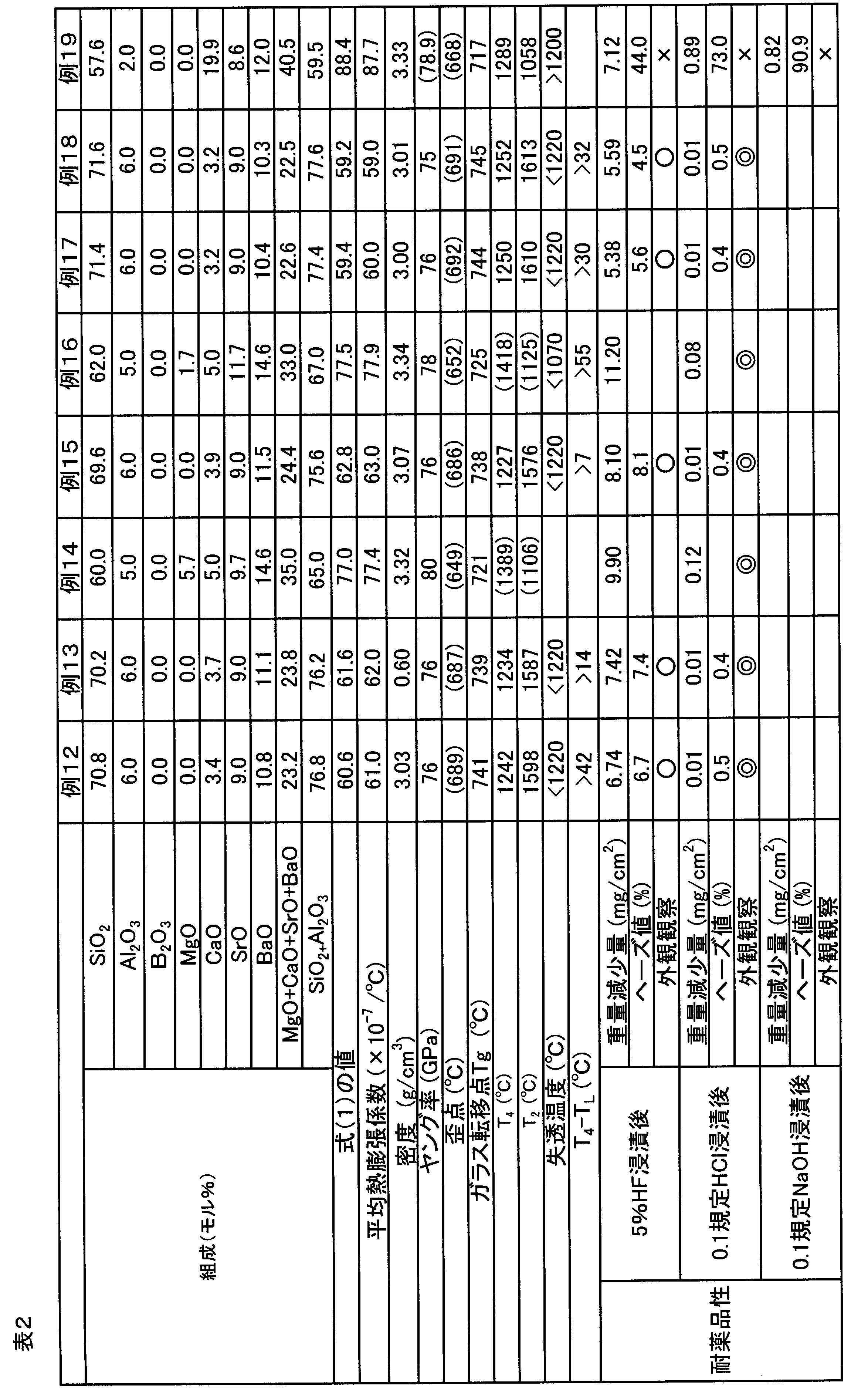
式(1)は、ガラス組成と50℃~350℃での平均熱膨張係数の関係を表す回帰式である。この回帰式は、SiO2の含有量、Al2O3の含有量、B2O3の含有量、MgOの含有量、CaOの含有量、SrOの含有量、BaOの含有量がそれぞれ異なる約100個のガラスの50℃~350℃での平均熱膨張係数を測定することにより得た。式(1)の値が56~90であれば、50℃~350℃での平均熱膨張係数を56~90(×10-7/℃)の範囲にしやすい。
上記式において、T3500cm-1は、波数(wave number)3500cm-1の光の透過率(%)であり、T4000cm-1は、波数4000cm-1の光の透過率(%)であり、tは、ガラス基板の厚さ(mm)である。
JIS R3102(1995年)に規定されている方法に従い、示差熱膨張計(TMA)を用いて測定した。測定温度範囲は50~350℃で、単位を10-7/℃として表した。
泡を含まない約20gのガラス塊をアルキメデス法によって測定した。
厚さ0.5~10mmのガラスについて、超音波パルス法により測定した。
JIS R3103-2(2001年)に規定されている方法に従い測定した。(ガラス転移点Tg)
JIS R3103-3(2001年)に規定されている方法に従い、TMAを用いて測定した。
回転粘度計を用いて粘度を測定し、104dPa・sとなるときの温度T4(℃)を測定した。
回転粘度計を用いて粘度を測定し、102dPa・sとなるときの温度T2(℃)を測定した。
失透温度は、白金製皿に粉砕されたガラス粒子を入れ、一定温度に制御された電気炉中で17時間熱処理を行い、熱処理後の光学顕微鏡観察によって、ガラス表面および内部に結晶が析出しない温度の最大値である。
得られたガラスを40mm×40mm×1mmとなるようにダイヤモンド砥石、酸化セリウム砥石、および酸化セリウム砥粒を用いて鏡面加工した。HClに対する耐久性を調べるために、鏡面加工したガラスを直交する2辺を支持するようフッ素樹脂製の治具の上に設置し、蓋付きのフッ素樹脂製容器に入れた温度90℃、濃度0.1規定の330mlのHCl溶液に20時間浸漬させた。ガラスを取り出し、イオン交換水で表面を洗い流し、イオン交換水中で10分間超音波洗浄を行い、治具の上で自然乾燥させた。その後、外観観察を行い、重量を測定し、浸漬前後での単位面積当たりの重量減少量(単位:mg/cm2)を測定した。さらに、JIS K7136(2000年)に規定されている方法に従い、ヘーズメータ(スガ試験機社製タッチパネル式ヘーズコンピュータ、型番:HZ-2)を用いて、浸漬後のガラスのヘーズ率(単位:%)を測定した。
〔評価指標〕
◎:ガラス板全体が透明
○:ガラス板の透明である部分が全体の90%以上
△:ガラス板の透明である部分が全体の90%未満またはガラス板表面の一部が変質している
×:ガラス板全体が白濁している

20、50 剥離層
30、70 積層基板
60 樹脂
G1、G2 ガラス基板
Claims (20)
- 母組成として、酸化物基準のモル百分率表示で、
SiO2:58~75%、
Al2O3:4.5~7%、
B2O3:0~6%、
MgO:0~6%、
CaO:1~6%、
SrO:5~20%、
BaO:9~20%、
MgO+CaO+SrO+BaO:15~40%を含み、
アルカリ金属酸化物の含有量が酸化物基準のモル百分率表示で0~0.1%であり、
50℃~350℃での平均熱膨張係数αが56~90(×10-7/℃)であり、
温度90℃、濃度0.1NのNaOH水溶液に20時間浸漬したときの単位面積当たりの重量減少が3mg/cm2以下である、ガラス基板。 - 温度90℃、濃度0.1規定のNaOH溶液に20時間浸漬後のヘーズ率が50%以下である請求項1に記載のガラス基板。
- 酸化物基準のモル百分率表示で各酸化物の含有量の割合の関係を表した下記式(1)によって求められる値が56~90となる請求項1または2に記載のガラス基板。
0.174×(SiO2の含有量)-0.012×(Al2O3の含有量)+0.317×(B2O3の含有量)+0.988×(MgOの含有量)+1.715×(CaOの含有量)+2.011×(SrOの含有量)+2.251×(BaOの含有量)+0.076 (1) - 酸化物基準のモル百分率表示で、SiO2およびAl2O3の合計含有量が65%以上である請求項1~3のいずれか1項に記載のガラス基板。
- 温度90℃、濃度0.1規定のHCl溶液に20時間浸漬後の単位面積当たりの重量減少量が0.3mg/cm2以下である請求項1~4のいずれか一項に記載のガラス基板。
- 温度25℃、濃度5%のHF溶液に20分浸漬後の単位面積当たりの重量減少量が13mg/cm2以下である請求項1~5のいずれか一項に記載のガラス基板。
- 温度90℃、濃度0.1規定のHCl溶液に20時間浸漬後の厚さ1mmでのヘーズ率が50%以下である請求項1~6のいずれか一項に記載のガラス基板。
- 温度25℃、濃度5%のHF溶液に20分浸漬後のヘーズ率が50%以下である請求項1~7のいずれか一項に記載のガラス基板。
- 失透温度が1250℃以下である請求項1~8のいずれか一項に記載のガラス基板。
- 酸化物基準の質量百万分率表示で、Fe2O3の含有量が200ppm以下である請求項1~9のいずれか一項に記載のガラス基板。
- ヤング率が65GPa以上である請求項1~10のいずれか一項に記載のガラス基板。
- 厚さが2.0mm以下である請求項1~11のいずれか一項に記載のガラス基板。
- 面積が70~2500cm2である請求項1~12のいずれか一項に記載のガラス基板。
- 前記ガラス基板の形状が円形である請求項1~13のいずれか一項に記載のガラス基板。
- 前記ガラス基板のβ-OHが0.05~0.65mm-1である請求項1~14のいずれか一項に記載のガラス基板。
- 前記ガラス基板の少なくとも一の主表面に遮光膜を有する請求項1~15のいずれか一項に記載のガラス基板。
- ガラス転移点(Tg)が680℃以上である請求項1~16のいずれか一項に記載のガラス基板。
- ファンアウト型のウェハレベルパッケージ用のガラス基板である請求項1~17のいずれか一項に記載のガラス基板。
- 請求項1~18のいずれか一項に記載のガラス基板と、シリコン基板とが積層されて形成される積層基板。
- 請求項19に記載の積層基板を構成するガラス基板に他のガラス基板を貼り合わせることにより形成される積層体。
Applications Claiming Priority (3)
| Application Number | Priority Date | Filing Date | Title |
|---|---|---|---|
| JP2015196548 | 2015-10-02 | ||
| JP2015196548 | 2015-10-02 | ||
| JP2020114272A JP6992847B2 (ja) | 2015-10-02 | 2020-07-01 | ガラス基板、積層基板、および積層体 |
Related Parent Applications (1)
| Application Number | Title | Priority Date | Filing Date |
|---|---|---|---|
| JP2020114272A Division JP6992847B2 (ja) | 2015-10-02 | 2020-07-01 | ガラス基板、積層基板、および積層体 |
Publications (2)
| Publication Number | Publication Date |
|---|---|
| JP2022027842A JP2022027842A (ja) | 2022-02-14 |
| JP7298075B2 true JP7298075B2 (ja) | 2023-06-27 |
Family
ID=58423907
Family Applications (3)
| Application Number | Title | Priority Date | Filing Date |
|---|---|---|---|
| JP2017543478A Active JP6729596B2 (ja) | 2015-10-02 | 2016-09-28 | ガラス基板、積層基板、および積層体 |
| JP2020114272A Active JP6992847B2 (ja) | 2015-10-02 | 2020-07-01 | ガラス基板、積層基板、および積層体 |
| JP2021198042A Active JP7298075B2 (ja) | 2015-10-02 | 2021-12-06 | ガラス基板、積層基板、および積層体 |
Family Applications Before (2)
| Application Number | Title | Priority Date | Filing Date |
|---|---|---|---|
| JP2017543478A Active JP6729596B2 (ja) | 2015-10-02 | 2016-09-28 | ガラス基板、積層基板、および積層体 |
| JP2020114272A Active JP6992847B2 (ja) | 2015-10-02 | 2020-07-01 | ガラス基板、積層基板、および積層体 |
Country Status (6)
| Country | Link |
|---|---|
| US (2) | US11180407B2 (ja) |
| JP (3) | JP6729596B2 (ja) |
| KR (3) | KR102636900B1 (ja) |
| CN (3) | CN117865460A (ja) |
| TW (1) | TWI725056B (ja) |
| WO (1) | WO2017057446A1 (ja) |
Families Citing this family (6)
| Publication number | Priority date | Publication date | Assignee | Title |
|---|---|---|---|---|
| KR102602900B1 (ko) * | 2015-12-28 | 2023-11-16 | 에이지씨 가부시키가이샤 | 유리 기판, 적층 기판, 적층체, 및 반도체 패키지의 제조 방법 |
| KR20190054068A (ko) * | 2016-09-16 | 2019-05-21 | 에이지씨 가부시키가이샤 | 유리 기판 및 적층 기판 |
| JP2019080457A (ja) * | 2017-10-26 | 2019-05-23 | 日本発條株式会社 | 非接触給電装置 |
| US10829412B2 (en) | 2018-07-13 | 2020-11-10 | Corning Incorporated | Carriers for microelectronics fabrication |
| CN112543746B (zh) * | 2019-07-23 | 2021-12-28 | Agc株式会社 | 玻璃 |
| WO2022191020A1 (ja) * | 2021-03-12 | 2022-09-15 | 株式会社村田製作所 | ガラスセラミック材料、積層体、及び、電子部品 |
Citations (5)
| Publication number | Priority date | Publication date | Assignee | Title |
|---|---|---|---|---|
| JP2003112942A (ja) | 2001-10-03 | 2003-04-18 | Nippon Electric Glass Co Ltd | 電界放射型ディスプレイ用ガラス基板 |
| WO2008136316A1 (ja) | 2007-04-26 | 2008-11-13 | Alps Electric Co., Ltd. | 積層基板構造体及びその製造方法 |
| JP2010218942A (ja) | 2009-03-18 | 2010-09-30 | Panasonic Corp | プラズマディスプレイパネルの製造方法 |
| JP2014500848A (ja) | 2010-12-08 | 2014-01-16 | ショット アクチエンゲゼルシャフト | ホウ素フリー汎用ガラス |
| JP2015078113A (ja) | 2013-09-12 | 2015-04-23 | 日本電気硝子株式会社 | 支持ガラス基板及びこれを用いた搬送体 |
Family Cites Families (27)
| Publication number | Priority date | Publication date | Assignee | Title |
|---|---|---|---|---|
| JP2926800B2 (ja) * | 1989-11-28 | 1999-07-28 | 旭硝子株式会社 | ガラス組成物 |
| JPH05182609A (ja) * | 1991-12-27 | 1993-07-23 | Sharp Corp | 画像表示装置 |
| US5459109A (en) * | 1994-09-19 | 1995-10-17 | Corning Incorporated | Substrate glasses for plasma displays |
| US5741746A (en) | 1995-03-02 | 1998-04-21 | Kohli; Jeffrey T. | Glasses for display panels |
| US5634585A (en) * | 1995-10-23 | 1997-06-03 | Micron Display Technology, Inc. | Method for aligning and assembling spaced components |
| JPH10139467A (ja) * | 1996-11-12 | 1998-05-26 | Asahi Glass Co Ltd | 無アルカリガラス及びフラットディスプレイパネル |
| JP3549141B2 (ja) * | 1997-04-21 | 2004-08-04 | 大日本スクリーン製造株式会社 | 基板処理装置および基板保持装置 |
| DE19739912C1 (de) * | 1997-09-11 | 1998-12-10 | Schott Glas | Alkalifreies Aluminoborosilicatglas und dessen Verwendung |
| JP2003026442A (ja) * | 2001-07-13 | 2003-01-29 | Nippon Electric Glass Co Ltd | 電界放射型ディスプレイ用ガラス基板 |
| JP2003054985A (ja) * | 2001-08-09 | 2003-02-26 | Nippon Electric Glass Co Ltd | 電界放射型ディスプレイ用ガラス基板 |
| US7050271B2 (en) | 2002-11-28 | 2006-05-23 | Tdk Corporation | Actuator having doped silicon arms and method of making the same |
| JP2004193574A (ja) * | 2002-11-28 | 2004-07-08 | Tdk Corp | アクチュエータ及びその製造方法 |
| JP4507560B2 (ja) * | 2003-10-30 | 2010-07-21 | 日本電気株式会社 | 薄膜デバイス基板の製造方法 |
| CN1898168B (zh) * | 2003-12-26 | 2012-08-01 | 旭硝子株式会社 | 无碱玻璃、其制造方法及液晶显示板 |
| JP4803643B2 (ja) * | 2005-06-15 | 2011-10-26 | Hoya株式会社 | ガラス部材、それを用いた製品およびその製造方法 |
| JP2008159449A (ja) * | 2006-12-25 | 2008-07-10 | Canon Inc | 表示装置 |
| JP5334411B2 (ja) * | 2007-12-30 | 2013-11-06 | 株式会社フジクラ | 貼り合わせ基板および貼り合せ基板を用いた半導体装置の製造方法 |
| JP2009231635A (ja) * | 2008-03-24 | 2009-10-08 | Shinko Electric Ind Co Ltd | 配線基板及びその製造方法、及び半導体装置及びその製造方法 |
| SG172796A1 (en) * | 2009-02-02 | 2011-08-29 | Asahi Glass Co Ltd | Glass substrate for semiconductor device member, and process for producing glass substrate for semiconductor device member |
| MY177073A (en) * | 2010-04-27 | 2020-09-04 | Agc Inc | Method for producing magnetic disk, and glass substrate for information recording medium |
| JP2012064710A (ja) * | 2010-09-15 | 2012-03-29 | Asahi Glass Co Ltd | 半導体素子の製造方法 |
| CN103347832A (zh) * | 2011-02-08 | 2013-10-09 | 旭硝子株式会社 | 玻璃组合物及使用玻璃组合物的太阳能电池用玻璃基板、以及显示面板用玻璃基板 |
| CN103035461B (zh) * | 2011-09-30 | 2016-04-13 | 清华大学 | 电子发射装置及显示装置 |
| JP5333572B2 (ja) * | 2011-12-22 | 2013-11-06 | 富士通セミコンダクター株式会社 | 半導体素子の実装方法及び半導体装置の製造方法 |
| JP6277617B2 (ja) * | 2012-07-23 | 2018-02-14 | セントラル硝子株式会社 | 接着性組成物およびその接着方法、および接着後の剥離方法 |
| JP5797222B2 (ja) * | 2012-10-02 | 2015-10-21 | AvanStrate株式会社 | ガラス基板の製造方法および製造装置 |
| JP6547995B2 (ja) * | 2013-04-25 | 2019-07-24 | 日本電気硝子株式会社 | 高屈折率ガラス基板 |
-
2016
- 2016-09-28 KR KR1020187008966A patent/KR102636900B1/ko active Active
- 2016-09-28 CN CN202311811679.8A patent/CN117865460A/zh active Pending
- 2016-09-28 CN CN201680058008.0A patent/CN108137379A/zh active Pending
- 2016-09-28 CN CN202311814406.9A patent/CN117865461A/zh active Pending
- 2016-09-28 JP JP2017543478A patent/JP6729596B2/ja active Active
- 2016-09-28 KR KR1020247004385A patent/KR102769729B1/ko active Active
- 2016-09-28 KR KR1020257004561A patent/KR20250026386A/ko active Pending
- 2016-09-28 WO PCT/JP2016/078598 patent/WO2017057446A1/ja not_active Ceased
- 2016-09-30 TW TW105131530A patent/TWI725056B/zh active
-
2018
- 2018-03-29 US US15/939,631 patent/US11180407B2/en active Active
-
2020
- 2020-07-01 JP JP2020114272A patent/JP6992847B2/ja active Active
-
2021
- 2021-09-21 US US17/480,440 patent/US11753330B2/en active Active
- 2021-12-06 JP JP2021198042A patent/JP7298075B2/ja active Active
Patent Citations (5)
| Publication number | Priority date | Publication date | Assignee | Title |
|---|---|---|---|---|
| JP2003112942A (ja) | 2001-10-03 | 2003-04-18 | Nippon Electric Glass Co Ltd | 電界放射型ディスプレイ用ガラス基板 |
| WO2008136316A1 (ja) | 2007-04-26 | 2008-11-13 | Alps Electric Co., Ltd. | 積層基板構造体及びその製造方法 |
| JP2010218942A (ja) | 2009-03-18 | 2010-09-30 | Panasonic Corp | プラズマディスプレイパネルの製造方法 |
| JP2014500848A (ja) | 2010-12-08 | 2014-01-16 | ショット アクチエンゲゼルシャフト | ホウ素フリー汎用ガラス |
| JP2015078113A (ja) | 2013-09-12 | 2015-04-23 | 日本電気硝子株式会社 | 支持ガラス基板及びこれを用いた搬送体 |
Also Published As
| Publication number | Publication date |
|---|---|
| CN117865461A (zh) | 2024-04-12 |
| JP2020176053A (ja) | 2020-10-29 |
| KR20240023683A (ko) | 2024-02-22 |
| CN117865460A (zh) | 2024-04-12 |
| JP6992847B2 (ja) | 2022-01-13 |
| US20180222787A1 (en) | 2018-08-09 |
| CN108137379A (zh) | 2018-06-08 |
| KR102636900B1 (ko) | 2024-02-16 |
| WO2017057446A1 (ja) | 2017-04-06 |
| US11753330B2 (en) | 2023-09-12 |
| JPWO2017057446A1 (ja) | 2018-07-19 |
| JP6729596B2 (ja) | 2020-07-22 |
| KR20250026386A (ko) | 2025-02-25 |
| KR20180061203A (ko) | 2018-06-07 |
| US11180407B2 (en) | 2021-11-23 |
| KR102769729B1 (ko) | 2025-02-20 |
| JP2022027842A (ja) | 2022-02-14 |
| TWI725056B (zh) | 2021-04-21 |
| TW201730123A (zh) | 2017-09-01 |
| US20220002183A1 (en) | 2022-01-06 |
Similar Documents
| Publication | Publication Date | Title |
|---|---|---|
| JP7298075B2 (ja) | ガラス基板、積層基板、および積層体 | |
| KR102515348B1 (ko) | 유리 기판 및 적층 기판 | |
| JP6604337B2 (ja) | ガラス基板、積層基板、およびガラス基板の製造方法 | |
| JP6819613B2 (ja) | ガラス基板、積層基板、積層体、および半導体パッケージの製造方法 | |
| JP6879308B2 (ja) | ガラス基板、および積層基板 | |
| TWI737735B (zh) | 無鹼玻璃基板、積層基板、及玻璃基板之製造方法 | |
| WO2018025727A1 (ja) | 無アルカリガラス基板、積層基板、およびガラス基板の製造方法 | |
| JP2020007184A (ja) | 半導体用支持基板 |
Legal Events
| Date | Code | Title | Description |
|---|---|---|---|
| A621 | Written request for application examination |
Free format text: JAPANESE INTERMEDIATE CODE: A621 Effective date: 20211206 |
|
| A977 | Report on retrieval |
Free format text: JAPANESE INTERMEDIATE CODE: A971007 Effective date: 20221216 |
|
| A131 | Notification of reasons for refusal |
Free format text: JAPANESE INTERMEDIATE CODE: A131 Effective date: 20230110 |
|
| A521 | Request for written amendment filed |
Free format text: JAPANESE INTERMEDIATE CODE: A523 Effective date: 20230208 |
|
| TRDD | Decision of grant or rejection written | ||
| A01 | Written decision to grant a patent or to grant a registration (utility model) |
Free format text: JAPANESE INTERMEDIATE CODE: A01 Effective date: 20230509 |
|
| A61 | First payment of annual fees (during grant procedure) |
Free format text: JAPANESE INTERMEDIATE CODE: A61 Effective date: 20230522 |
|
| R150 | Certificate of patent or registration of utility model |
Ref document number: 7298075 Country of ref document: JP Free format text: JAPANESE INTERMEDIATE CODE: R150 |