JP7302247B2 - 画像形成装置 - Google Patents
画像形成装置 Download PDFInfo
- Publication number
- JP7302247B2 JP7302247B2 JP2019074188A JP2019074188A JP7302247B2 JP 7302247 B2 JP7302247 B2 JP 7302247B2 JP 2019074188 A JP2019074188 A JP 2019074188A JP 2019074188 A JP2019074188 A JP 2019074188A JP 7302247 B2 JP7302247 B2 JP 7302247B2
- Authority
- JP
- Japan
- Prior art keywords
- charging
- image
- current
- image forming
- charging member
- Prior art date
- Legal status (The legal status is an assumption and is not a legal conclusion. Google has not performed a legal analysis and makes no representation as to the accuracy of the status listed.)
- Active
Links
- 230000006866 deterioration Effects 0.000 claims description 63
- 230000008030 elimination Effects 0.000 claims description 40
- 238000003379 elimination reaction Methods 0.000 claims description 40
- 230000003068 static effect Effects 0.000 claims description 40
- 230000015572 biosynthetic process Effects 0.000 claims description 20
- 238000007599 discharging Methods 0.000 claims description 12
- 230000003472 neutralizing effect Effects 0.000 claims description 8
- 238000001514 detection method Methods 0.000 claims description 4
- 230000007423 decrease Effects 0.000 claims description 3
- 238000011144 upstream manufacturing Methods 0.000 claims description 2
- 108091008695 photoreceptors Proteins 0.000 description 54
- 238000012546 transfer Methods 0.000 description 34
- 238000012937 correction Methods 0.000 description 17
- 238000004140 cleaning Methods 0.000 description 12
- 238000012545 processing Methods 0.000 description 11
- 238000010586 diagram Methods 0.000 description 10
- 238000000034 method Methods 0.000 description 10
- 230000008569 process Effects 0.000 description 10
- 230000006870 function Effects 0.000 description 7
- 239000000654 additive Substances 0.000 description 6
- 230000000996 additive effect Effects 0.000 description 6
- 230000008859 change Effects 0.000 description 6
- 229920001971 elastomer Polymers 0.000 description 4
- 238000011109 contamination Methods 0.000 description 2
- 230000007547 defect Effects 0.000 description 2
- 238000006386 neutralization reaction Methods 0.000 description 2
- 230000003287 optical effect Effects 0.000 description 2
- WFKWXMTUELFFGS-UHFFFAOYSA-N tungsten Chemical compound [W] WFKWXMTUELFFGS-UHFFFAOYSA-N 0.000 description 2
- 229910052721 tungsten Inorganic materials 0.000 description 2
- 239000010937 tungsten Substances 0.000 description 2
- 229920006311 Urethane elastomer Polymers 0.000 description 1
- 239000002801 charged material Substances 0.000 description 1
- 230000002950 deficient Effects 0.000 description 1
- 230000003111 delayed effect Effects 0.000 description 1
- 238000011161 development Methods 0.000 description 1
- 230000001678 irradiating effect Effects 0.000 description 1
- 239000000463 material Substances 0.000 description 1
- 230000007246 mechanism Effects 0.000 description 1
- 229910052751 metal Inorganic materials 0.000 description 1
- 239000002184 metal Substances 0.000 description 1
- 238000012986 modification Methods 0.000 description 1
- 230000004048 modification Effects 0.000 description 1
- 230000002093 peripheral effect Effects 0.000 description 1
- 230000001737 promoting effect Effects 0.000 description 1
- 230000007704 transition Effects 0.000 description 1
Images






Classifications
-
- G—PHYSICS
- G03—PHOTOGRAPHY; CINEMATOGRAPHY; ANALOGOUS TECHNIQUES USING WAVES OTHER THAN OPTICAL WAVES; ELECTROGRAPHY; HOLOGRAPHY
- G03G—ELECTROGRAPHY; ELECTROPHOTOGRAPHY; MAGNETOGRAPHY
- G03G15/00—Apparatus for electrographic processes using a charge pattern
- G03G15/02—Apparatus for electrographic processes using a charge pattern for laying down a uniform charge, e.g. for sensitising; Corona discharge devices
- G03G15/0266—Arrangements for controlling the amount of charge
-
- G—PHYSICS
- G03—PHOTOGRAPHY; CINEMATOGRAPHY; ANALOGOUS TECHNIQUES USING WAVES OTHER THAN OPTICAL WAVES; ELECTROGRAPHY; HOLOGRAPHY
- G03G—ELECTROGRAPHY; ELECTROPHOTOGRAPHY; MAGNETOGRAPHY
- G03G15/00—Apparatus for electrographic processes using a charge pattern
- G03G15/02—Apparatus for electrographic processes using a charge pattern for laying down a uniform charge, e.g. for sensitising; Corona discharge devices
- G03G15/0208—Apparatus for electrographic processes using a charge pattern for laying down a uniform charge, e.g. for sensitising; Corona discharge devices by contact, friction or induction, e.g. liquid charging apparatus
- G03G15/0216—Apparatus for electrographic processes using a charge pattern for laying down a uniform charge, e.g. for sensitising; Corona discharge devices by contact, friction or induction, e.g. liquid charging apparatus by bringing a charging member into contact with the member to be charged, e.g. roller, brush chargers
-
- G—PHYSICS
- G03—PHOTOGRAPHY; CINEMATOGRAPHY; ANALOGOUS TECHNIQUES USING WAVES OTHER THAN OPTICAL WAVES; ELECTROGRAPHY; HOLOGRAPHY
- G03G—ELECTROGRAPHY; ELECTROPHOTOGRAPHY; MAGNETOGRAPHY
- G03G15/00—Apparatus for electrographic processes using a charge pattern
- G03G15/02—Apparatus for electrographic processes using a charge pattern for laying down a uniform charge, e.g. for sensitising; Corona discharge devices
- G03G15/0258—Apparatus for electrographic processes using a charge pattern for laying down a uniform charge, e.g. for sensitising; Corona discharge devices provided with means for the maintenance of the charging apparatus, e.g. cleaning devices, ozone removing devices G03G15/0225, G03G15/0291 takes precedence
-
- G—PHYSICS
- G03—PHOTOGRAPHY; CINEMATOGRAPHY; ANALOGOUS TECHNIQUES USING WAVES OTHER THAN OPTICAL WAVES; ELECTROGRAPHY; HOLOGRAPHY
- G03G—ELECTROGRAPHY; ELECTROPHOTOGRAPHY; MAGNETOGRAPHY
- G03G15/00—Apparatus for electrographic processes using a charge pattern
- G03G15/02—Apparatus for electrographic processes using a charge pattern for laying down a uniform charge, e.g. for sensitising; Corona discharge devices
- G03G15/0275—Arrangements for controlling the area of the photoconductor to be charged
-
- G—PHYSICS
- G03—PHOTOGRAPHY; CINEMATOGRAPHY; ANALOGOUS TECHNIQUES USING WAVES OTHER THAN OPTICAL WAVES; ELECTROGRAPHY; HOLOGRAPHY
- G03G—ELECTROGRAPHY; ELECTROPHOTOGRAPHY; MAGNETOGRAPHY
- G03G15/00—Apparatus for electrographic processes using a charge pattern
- G03G15/50—Machine control of apparatus for electrographic processes using a charge pattern, e.g. regulating differents parts of the machine, multimode copiers, microprocessor control
- G03G15/5004—Power supply control, e.g. power-saving mode, automatic power turn-off
-
- G—PHYSICS
- G03—PHOTOGRAPHY; CINEMATOGRAPHY; ANALOGOUS TECHNIQUES USING WAVES OTHER THAN OPTICAL WAVES; ELECTROGRAPHY; HOLOGRAPHY
- G03G—ELECTROGRAPHY; ELECTROPHOTOGRAPHY; MAGNETOGRAPHY
- G03G15/00—Apparatus for electrographic processes using a charge pattern
- G03G15/50—Machine control of apparatus for electrographic processes using a charge pattern, e.g. regulating differents parts of the machine, multimode copiers, microprocessor control
- G03G15/5016—User-machine interface; Display panels; Control console
-
- G—PHYSICS
- G03—PHOTOGRAPHY; CINEMATOGRAPHY; ANALOGOUS TECHNIQUES USING WAVES OTHER THAN OPTICAL WAVES; ELECTROGRAPHY; HOLOGRAPHY
- G03G—ELECTROGRAPHY; ELECTROPHOTOGRAPHY; MAGNETOGRAPHY
- G03G2215/00—Apparatus for electrophotographic processes
- G03G2215/02—Arrangements for laying down a uniform charge
- G03G2215/021—Arrangements for laying down a uniform charge by contact, friction or induction
- G03G2215/025—Arrangements for laying down a uniform charge by contact, friction or induction using contact charging means having lateral dimensions related to other apparatus means, e.g. photodrum, developing roller
-
- G—PHYSICS
- G03—PHOTOGRAPHY; CINEMATOGRAPHY; ANALOGOUS TECHNIQUES USING WAVES OTHER THAN OPTICAL WAVES; ELECTROGRAPHY; HOLOGRAPHY
- G03G—ELECTROGRAPHY; ELECTROPHOTOGRAPHY; MAGNETOGRAPHY
- G03G2215/00—Apparatus for electrophotographic processes
- G03G2215/04—Arrangements for exposing and producing an image
- G03G2215/0429—Changing or enhancing the image
- G03G2215/0431—Producing a clean non-image area, i.e. avoiding show-around effects
- G03G2215/0448—Charge-erasing means for the non-image area
- G03G2215/0463—Exposure lamp used for scanning
Landscapes
- Physics & Mathematics (AREA)
- Engineering & Computer Science (AREA)
- General Physics & Mathematics (AREA)
- Plasma & Fusion (AREA)
- Microelectronics & Electronic Packaging (AREA)
- Electrostatic Charge, Transfer And Separation In Electrography (AREA)
- Control Or Security For Electrophotography (AREA)
- Discharging, Photosensitive Material Shape In Electrophotography (AREA)
Description
Claims (11)
- 記録媒体に転写される像を保持する像保持体と、
前記像保持体に接して前記像保持体を帯電する帯電部材と、
前記像保持体を除電する除電手段と、
前記帯電部材に流れる電流を検出する電流検出手段と、
前記像保持体の表面に帯電領域と、前記除電手段により除電領域を形成する形成手段と、
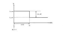
前記除電領域に前記帯電部材から電圧を印加して流れる前記電流である第1電流と、前記帯電領域に前記帯電部材から電圧を印加して流れる前記電流である第2電流との電流差に基づいて、前記帯電部材の劣化状態を取得する状態取得手段と、を含む、
画像形成装置。 - 請求項1に記載の画像形成装置おいて、
前記像保持体は回転し、
前記除電手段は、前記回転の方向における前記帯電部材よりも上流側に配置され、
前記形成手段は、前記帯電部材により前記像保持体を帯電させた後、前記除電手段のオフとオンを切り替えることにより、前記像保持体の表面に前記帯電領域と前記除電領域を形成する、
画像形成装置。 - 請求項1または2に記載の画像形成装置おいて、
前記帯電部材の劣化状態に基づいて、画像形成時における前記帯電部材から前記像保持体に印加する電圧を変更する変更手段、を含む、
画像形成装置。 - 請求項1または2に記載の画像形成装置おいて、
前記電流差に基づいて、画像形成時における前記帯電部材から前記像保持体に印加する電圧を変更する変更手段、を含む、
画像形成装置。 - 請求項4に記載の画像形成装置おいて、
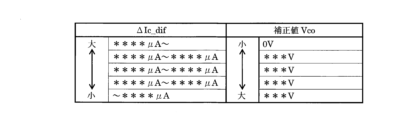
前記変更手段は、前記電流差が小さいほど、画像形成時における前記帯電部材から前記像保持体に印加する電圧を高くするように変更する、
画像形成装置。 - 請求項1または2に記載の画像形成装置おいて、
前記帯電部材の劣化状態に基づいた前記帯電部材の劣化レベルを表示する表示手段、を含む、
画像形成装置。 - 請求項1または2に記載の画像形成装置おいて、
前記電流差に基づいた前記帯電部材の劣化レベルを表示する表示手段、を含む、
画像形成装置。 - 請求項7に記載の画像形成装置おいて、
前記表示手段は、前記電流差が小さいほど、前記帯電部材の劣化が進んでいることを示す前記劣化レベルを表示する、
画像形成装置。 - 請求項1または2に記載の画像形成装置おいて、
前記電流差が予め定められた値より小さい場合には、警告を表示する表示手段、を含む、
画像形成装置。 - 請求項1または2に記載の画像形成装置おいて、
前記形成手段が前記像保持体の表面に前記帯電領域と前記除電領域を形成した後、画像形成動作を開始するまでの時間が予め定められた時間より短い場合には、前記除電手段により前記像保持体の表面を除電する、
画像形成装置。 - 記録媒体に転写される像を保持する像保持体と、
前記像保持体に接して前記像保持体を帯電する帯電部材と、
前記像保持体を除電する除電手段と、
前記帯電部材に流れる電流を検出する電流検出手段と、
前記像保持体の表面に帯電領域と、前記除電手段により除電領域を形成する形成手段と、
前記除電領域に前記帯電部材から電圧を印加して流れる前記電流である第1電流と、前記帯電領域に前記帯電部材から電圧を印加して流れる前記電流である第2電流との電流差に基づいて、画像形成時における前記帯電部材から前記像保持体に印加する電圧を変更する変更手段と、を含む、
画像形成装置。
Priority Applications (2)
| Application Number | Priority Date | Filing Date | Title |
|---|---|---|---|
| JP2019074188A JP7302247B2 (ja) | 2019-04-09 | 2019-04-09 | 画像形成装置 |
| US16/727,014 US10859939B2 (en) | 2019-04-09 | 2019-12-26 | Image forming apparatus |
Applications Claiming Priority (1)
| Application Number | Priority Date | Filing Date | Title |
|---|---|---|---|
| JP2019074188A JP7302247B2 (ja) | 2019-04-09 | 2019-04-09 | 画像形成装置 |
Publications (2)
| Publication Number | Publication Date |
|---|---|
| JP2020173311A JP2020173311A (ja) | 2020-10-22 |
| JP7302247B2 true JP7302247B2 (ja) | 2023-07-04 |
Family
ID=72748561
Family Applications (1)
| Application Number | Title | Priority Date | Filing Date |
|---|---|---|---|
| JP2019074188A Active JP7302247B2 (ja) | 2019-04-09 | 2019-04-09 | 画像形成装置 |
Country Status (2)
| Country | Link |
|---|---|
| US (1) | US10859939B2 (ja) |
| JP (1) | JP7302247B2 (ja) |
Citations (1)
| Publication number | Priority date | Publication date | Assignee | Title |
|---|---|---|---|---|
| JP2017142302A (ja) | 2016-02-08 | 2017-08-17 | キヤノン株式会社 | 画像形成装置 |
Family Cites Families (5)
| Publication number | Priority date | Publication date | Assignee | Title |
|---|---|---|---|---|
| JP3330760B2 (ja) * | 1994-12-13 | 2002-09-30 | 松下電器産業株式会社 | 帯電装置 |
| JP5153245B2 (ja) * | 2007-07-26 | 2013-02-27 | キヤノン株式会社 | 画像形成装置 |
| JP5670374B2 (ja) | 2012-03-29 | 2015-02-18 | 株式会社沖データ | 画像形成装置、および画像形成プログラム |
| JP2015081975A (ja) * | 2013-10-22 | 2015-04-27 | 富士ゼロックス株式会社 | 帯電部材汚れの判定装置及び帯電部材汚れの判定プログラム |
| JP6844517B2 (ja) * | 2017-11-30 | 2021-03-17 | ブラザー工業株式会社 | 画像形成装置およびその制御方法ならびにプログラム |
-
2019
- 2019-04-09 JP JP2019074188A patent/JP7302247B2/ja active Active
- 2019-12-26 US US16/727,014 patent/US10859939B2/en active Active
Patent Citations (1)
| Publication number | Priority date | Publication date | Assignee | Title |
|---|---|---|---|---|
| JP2017142302A (ja) | 2016-02-08 | 2017-08-17 | キヤノン株式会社 | 画像形成装置 |
Also Published As
| Publication number | Publication date |
|---|---|
| US10859939B2 (en) | 2020-12-08 |
| JP2020173311A (ja) | 2020-10-22 |
| US20200326641A1 (en) | 2020-10-15 |
Similar Documents
| Publication | Publication Date | Title |
|---|---|---|
| CN102279539A (zh) | 图像形成装置及图像形成方法 | |
| JP5754961B2 (ja) | 画像形成装置 | |
| JP4898478B2 (ja) | 画像形成装置 | |
| JP7242376B2 (ja) | 画像形成装置 | |
| JP6855297B2 (ja) | 画像形成装置 | |
| JP7302247B2 (ja) | 画像形成装置 | |
| JP6418959B2 (ja) | 画像形成装置 | |
| JP2022063810A (ja) | 画像形成装置 | |
| JPH05197248A (ja) | プロセスコントロール安定化装置 | |
| JP7016649B2 (ja) | 画像形成装置 | |
| JP2018004917A (ja) | 画像形成装置 | |
| JP6589889B2 (ja) | 画像形成装置 | |
| JP2017076067A (ja) | 画像形成装置 | |
| JP2018189797A (ja) | 画像形成装置 | |
| JP6627797B2 (ja) | 画像形成装置 | |
| JP6958219B2 (ja) | 画像形成装置及び画像形成方法 | |
| JP6531734B2 (ja) | 画像形成装置 | |
| JP2016161932A (ja) | 画像形成装置 | |
| JP2006138991A (ja) | 画像形成装置 | |
| JP2008076792A (ja) | 画像形成装置 | |
| JP2019184847A (ja) | 画像形成装置 | |
| JP7240600B2 (ja) | 画像形成装置 | |
| JP2009008828A (ja) | 画像形成装置 | |
| JP2022092658A (ja) | 画像形成装置 | |
| JP6805976B2 (ja) | 画像形成装置 |
Legal Events
| Date | Code | Title | Description |
|---|---|---|---|
| A621 | Written request for application examination |
Free format text: JAPANESE INTERMEDIATE CODE: A621 Effective date: 20220228 |
|
| A977 | Report on retrieval |
Free format text: JAPANESE INTERMEDIATE CODE: A971007 Effective date: 20221228 |
|
| A131 | Notification of reasons for refusal |
Free format text: JAPANESE INTERMEDIATE CODE: A131 Effective date: 20230110 |
|
| A521 | Request for written amendment filed |
Free format text: JAPANESE INTERMEDIATE CODE: A523 Effective date: 20230306 |
|
| TRDD | Decision of grant or rejection written | ||
| A01 | Written decision to grant a patent or to grant a registration (utility model) |
Free format text: JAPANESE INTERMEDIATE CODE: A01 Effective date: 20230523 |
|
| A61 | First payment of annual fees (during grant procedure) |
Free format text: JAPANESE INTERMEDIATE CODE: A61 Effective date: 20230605 |
|
| R150 | Certificate of patent or registration of utility model |
Ref document number: 7302247 Country of ref document: JP Free format text: JAPANESE INTERMEDIATE CODE: R150 |