JP7307601B2 - マイクロ流路デバイス - Google Patents
マイクロ流路デバイス Download PDFInfo
- Publication number
- JP7307601B2 JP7307601B2 JP2019114044A JP2019114044A JP7307601B2 JP 7307601 B2 JP7307601 B2 JP 7307601B2 JP 2019114044 A JP2019114044 A JP 2019114044A JP 2019114044 A JP2019114044 A JP 2019114044A JP 7307601 B2 JP7307601 B2 JP 7307601B2
- Authority
- JP
- Japan
- Prior art keywords
- resin substrate
- bonding
- bonding region
- microchannel
- microfluidic device
- Prior art date
- Legal status (The legal status is an assumption and is not a legal conclusion. Google has not performed a legal analysis and makes no representation as to the accuracy of the status listed.)
- Active
Links
- 239000000758 substrate Substances 0.000 claims description 167
- 239000011347 resin Substances 0.000 claims description 111
- 229920005989 resin Polymers 0.000 claims description 111
- 239000004205 dimethyl polysiloxane Substances 0.000 claims description 30
- 229920000435 poly(dimethylsiloxane) Polymers 0.000 claims description 30
- -1 polydimethylsiloxane Polymers 0.000 claims description 9
- 239000012778 molding material Substances 0.000 claims description 7
- 238000010030 laminating Methods 0.000 claims description 5
- 230000000149 penetrating effect Effects 0.000 claims description 5
- 239000007788 liquid Substances 0.000 description 23
- 230000001050 lubricating effect Effects 0.000 description 20
- 238000000034 method Methods 0.000 description 18
- 239000000523 sample Substances 0.000 description 15
- 238000000465 moulding Methods 0.000 description 13
- 239000002184 metal Substances 0.000 description 12
- 229910052751 metal Inorganic materials 0.000 description 12
- 238000005323 electroforming Methods 0.000 description 11
- 238000005530 etching Methods 0.000 description 8
- 238000005304 joining Methods 0.000 description 8
- 229920002120 photoresistant polymer Polymers 0.000 description 7
- PXHVJJICTQNCMI-UHFFFAOYSA-N Nickel Chemical compound [Ni] PXHVJJICTQNCMI-UHFFFAOYSA-N 0.000 description 6
- 238000005452 bending Methods 0.000 description 6
- 229920001971 elastomer Polymers 0.000 description 5
- 239000000806 elastomer Substances 0.000 description 5
- 239000000463 material Substances 0.000 description 5
- 230000015572 biosynthetic process Effects 0.000 description 4
- 238000002347 injection Methods 0.000 description 4
- 239000007924 injection Substances 0.000 description 4
- 238000001746 injection moulding Methods 0.000 description 4
- 238000009832 plasma treatment Methods 0.000 description 4
- 238000012545 processing Methods 0.000 description 4
- LFQSCWFLJHTTHZ-UHFFFAOYSA-N Ethanol Chemical compound CCO LFQSCWFLJHTTHZ-UHFFFAOYSA-N 0.000 description 3
- KFZMGEQAYNKOFK-UHFFFAOYSA-N Isopropanol Chemical compound CC(C)O KFZMGEQAYNKOFK-UHFFFAOYSA-N 0.000 description 3
- OKKJLVBELUTLKV-UHFFFAOYSA-N Methanol Chemical compound OC OKKJLVBELUTLKV-UHFFFAOYSA-N 0.000 description 3
- 238000003475 lamination Methods 0.000 description 3
- 238000004519 manufacturing process Methods 0.000 description 3
- 229910052759 nickel Inorganic materials 0.000 description 3
- 238000000206 photolithography Methods 0.000 description 3
- 238000003825 pressing Methods 0.000 description 3
- XUIMIQQOPSSXEZ-UHFFFAOYSA-N Silicon Chemical compound [Si] XUIMIQQOPSSXEZ-UHFFFAOYSA-N 0.000 description 2
- 239000000853 adhesive Substances 0.000 description 2
- 239000012472 biological sample Substances 0.000 description 2
- 230000006835 compression Effects 0.000 description 2
- 238000007906 compression Methods 0.000 description 2
- 230000008602 contraction Effects 0.000 description 2
- 238000005520 cutting process Methods 0.000 description 2
- 238000006073 displacement reaction Methods 0.000 description 2
- 239000010408 film Substances 0.000 description 2
- 239000011521 glass Substances 0.000 description 2
- 238000012986 modification Methods 0.000 description 2
- 230000004048 modification Effects 0.000 description 2
- 150000002894 organic compounds Chemical class 0.000 description 2
- 238000000059 patterning Methods 0.000 description 2
- 229910052710 silicon Inorganic materials 0.000 description 2
- 239000010703 silicon Substances 0.000 description 2
- 238000009423 ventilation Methods 0.000 description 2
- 230000001070 adhesive effect Effects 0.000 description 1
- 230000001364 causal effect Effects 0.000 description 1
- 238000000748 compression moulding Methods 0.000 description 1
- 238000012790 confirmation Methods 0.000 description 1
- 238000003851 corona treatment Methods 0.000 description 1
- 208000028659 discharge Diseases 0.000 description 1
- 238000007599 discharging Methods 0.000 description 1
- 238000005516 engineering process Methods 0.000 description 1
- 238000010438 heat treatment Methods 0.000 description 1
- 239000012535 impurity Substances 0.000 description 1
- 230000001678 irradiating effect Effects 0.000 description 1
- 230000013011 mating Effects 0.000 description 1
- 238000002156 mixing Methods 0.000 description 1
- 238000006011 modification reaction Methods 0.000 description 1
- 230000035699 permeability Effects 0.000 description 1
- 238000005498 polishing Methods 0.000 description 1
- 230000002265 prevention Effects 0.000 description 1
- 230000001737 promoting effect Effects 0.000 description 1
- 230000002040 relaxant effect Effects 0.000 description 1
- 238000001179 sorption measurement Methods 0.000 description 1
- 238000004528 spin coating Methods 0.000 description 1
- 230000002194 synthesizing effect Effects 0.000 description 1
- 239000010409 thin film Substances 0.000 description 1
- 238000001721 transfer moulding Methods 0.000 description 1
- 239000012780 transparent material Substances 0.000 description 1
- 229910021642 ultra pure water Inorganic materials 0.000 description 1
- 239000012498 ultrapure water Substances 0.000 description 1
- 238000009834 vaporization Methods 0.000 description 1
- 230000008016 vaporization Effects 0.000 description 1
- 230000000007 visual effect Effects 0.000 description 1
- 238000003466 welding Methods 0.000 description 1
Images


Landscapes
- Lining Or Joining Of Plastics Or The Like (AREA)
- Physical Or Chemical Processes And Apparatus (AREA)
- Micromachines (AREA)
Description
第1接合領域と第2接合領域のいずれか一方若しくは双方の接合面のマイクロ流路が凹設された部位に接しない接合領域に、凹溝若しくはスリットからなる応力緩和部が格子状に形成されていることを特徴とする。
第1接合領域と第2接合領域のいずれか一方若しくは双方の接合面のマイクロ流路が凹設された部位に接しない接合領域の全体に、接合する第1樹脂基板と第2樹脂基板の側面に開口する多数の凹溝が形成されていることを特徴とする。
2 ベースシート(第1樹脂基板)
2A 第1接合領域
3 カバーシート(第2樹脂基板)
3A 第2接合領域
4 凹溝(応力緩和部)
5 マイクロ流路
20 マイクロ流路デバイス
21、22 マイクロ流路チップ
23、24 マイクロ流路
31、41 凹溝
Claims (10)
- 表面にマイクロ流路が凹設された平板状の第1樹脂基板と、
第1樹脂基板の表面上に積層される第2樹脂基板を備え、
第1樹脂基板の表面の前記マイクロ流路が凹設された部位を除く第1接合領域と、第1接合領域に積層方向で対向する第2樹脂基板の第2接合領域が一体に接合されるマイクロ流路デバイスであって、
第1接合領域と第2接合領域のいずれか一方若しくは双方の接合面の前記マイクロ流路が凹設された部位に接しない接合領域に、凹溝若しくはスリットからなる応力緩和部が格子状に形成されていることを特徴とするマイクロ流路デバイス。 - 前記接合面に応力緩和部が形成される第1樹脂基板若しくは第2樹脂基板は、PDMS(ポリジメチルシロキサン)で成形され、第1接合領域と第2接合領域の双方の接合面を表面改質して、第1接合領域と第2接合領域が一体に接合されることを特徴とする請求項1に記載のマイクロ流路デバイス。
- 第1樹脂基板は、PDMS(ポリジメチルシロキサン)を成形材料として成形され、前記応力緩和部は、第1接合領域の接合面に形成される凹溝からなることを特徴とする請求項1又は請求項2のいずれか1項に記載のマイクロ流路デバイス。
- 前記マイクロ流路と前記凹溝の前記第1接合領域の接合面からの深さが同一であることを特徴とする請求項3に記載のマイクロ流路デバイス。
- 前記応力緩和部は、接合する第1樹脂基板と第2樹脂基板の側面に開口する凹溝からなることを特徴とする請求項1乃至請求項4のいずれか1項に記載のマイクロ流路デバイス。
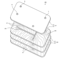
- それぞれ第1樹脂基板と第2樹脂基板を積層してなる複数のマイクロ流路チップが、積層方向に多段に積層されて一体に接合され、多段に積層された前記各マイクロ流路チップに形成されるマイクロ流路間は、第1樹脂基板若しくは第2樹脂基板を前記積層方向に貫通する貫通孔を介して連通するとともに、前記積層方向で対向するマイクロ流路チップの第1接合領域と第2接合領域の一方若しくは双方の接合面に、凹溝若しくはスリットからなる応力緩和部が格子状に形成されていることを特徴とする請求項1乃至請求項5のいずれか1項に記載のマイクロ流路デバイス。
- 表面にマイクロ流路が凹設された平板状の第1樹脂基板と、
第1樹脂基板の表面上に積層される第2樹脂基板を備え、
第1樹脂基板の表面の前記マイクロ流路が凹設された部位を除く第1接合領域と、第1接合領域に積層方向で対向する第2樹脂基板の第2接合領域が一体に接合されるマイクロ流路デバイスであって、
第1接合領域と第2接合領域のいずれか一方若しくは双方の接合面の前記マイクロ流路が凹設された部位に接しない接合領域の全体に、接合する第1樹脂基板と第2樹脂基板の側面に開口する多数の凹溝が形成されていることを特徴とするマイクロ流路デバイス。 - 第1樹脂基板と第2樹脂基板の少なくとも一方は、PDMS(ポリジメチルシロキサン)で成形され、第1接合領域と第2接合領域の双方の接合面を表面改質して、第1接合領域と第2接合領域が一体に接合されることを特徴とする請求項7に記載のマイクロ流路デバイス。
- 前記凹溝は、第1接合領域の接合面に形成され、前記マイクロ流路と前記凹溝の前記第1接合領域の接合面からの深さが同一であることを特徴とする請求項8に記載のマイクロ流路デバイス。
- それぞれ第1樹脂基板と第2樹脂基板を積層してなる複数のマイクロ流路チップが、積層方向に多段に積層されて一体に接合され、多段に積層された前記各マイクロ流路チップに形成されるマイクロ流路間は、第1樹脂基板若しくは第2樹脂基板を前記積層方向に貫通する貫通孔を介して連通するとともに、前記積層方向で対向するマイクロ流路チップの第1接合領域と第2接合領域の一方若しくは双方の接合面の全体に、接合する第1樹脂基板と第2樹脂基板の側面に開口する多数の凹溝が形成されていることを特徴とする請求項7乃至請求項9のいずれか1項に記載のマイクロ流路デバイス。
Priority Applications (1)
| Application Number | Priority Date | Filing Date | Title |
|---|---|---|---|
| PCT/JP2019/026250 WO2020021992A1 (ja) | 2018-07-24 | 2019-07-02 | マイクロ流路デバイスとマイクロ流路デバイスの製造方法 |
Applications Claiming Priority (2)
| Application Number | Priority Date | Filing Date | Title |
|---|---|---|---|
| JP2018138597 | 2018-07-24 | ||
| JP2018138597 | 2018-07-24 |
Publications (3)
| Publication Number | Publication Date |
|---|---|
| JP2020018999A JP2020018999A (ja) | 2020-02-06 |
| JP2020018999A5 JP2020018999A5 (ja) | 2022-07-12 |
| JP7307601B2 true JP7307601B2 (ja) | 2023-07-12 |
Family
ID=69589327
Family Applications (1)
| Application Number | Title | Priority Date | Filing Date |
|---|---|---|---|
| JP2019114044A Active JP7307601B2 (ja) | 2018-07-24 | 2019-06-19 | マイクロ流路デバイス |
Country Status (1)
| Country | Link |
|---|---|
| JP (1) | JP7307601B2 (ja) |
Citations (2)
| Publication number | Priority date | Publication date | Assignee | Title |
|---|---|---|---|---|
| JP2009236555A (ja) | 2008-03-26 | 2009-10-15 | Shimadzu Corp | 流体デバイス及びその製造方法 |
| JP2017225919A (ja) | 2016-06-21 | 2017-12-28 | 学校法人同志社 | 液滴製造キットおよび液滴の製造方法 |
Family Cites Families (4)
| Publication number | Priority date | Publication date | Assignee | Title |
|---|---|---|---|---|
| JP2006053064A (ja) * | 2004-08-12 | 2006-02-23 | Pentax Corp | マイクロ流体チップ及びその製造方法 |
| WO2009126826A1 (en) * | 2008-04-11 | 2009-10-15 | Fluidigm Corporation | Multilevel microfluidic systems and methods |
| WO2016050837A1 (en) * | 2014-09-30 | 2016-04-07 | Foss Analytical A/S | Method, device and system for hydrodynamic flow focusing |
| JP6394651B2 (ja) * | 2016-07-15 | 2018-09-26 | ウシオ電機株式会社 | 基板の貼り合わせ方法およびマイクロチップの製造方法 |
-
2019
- 2019-06-19 JP JP2019114044A patent/JP7307601B2/ja active Active
Patent Citations (2)
| Publication number | Priority date | Publication date | Assignee | Title |
|---|---|---|---|---|
| JP2009236555A (ja) | 2008-03-26 | 2009-10-15 | Shimadzu Corp | 流体デバイス及びその製造方法 |
| JP2017225919A (ja) | 2016-06-21 | 2017-12-28 | 学校法人同志社 | 液滴製造キットおよび液滴の製造方法 |
Also Published As
| Publication number | Publication date |
|---|---|
| JP2020018999A (ja) | 2020-02-06 |
Similar Documents
| Publication | Publication Date | Title |
|---|---|---|
| US5932315A (en) | Microfluidic structure assembly with mating microfeatures | |
| JP6531749B2 (ja) | 基板の貼り合わせ方法、並びに、マイクロチップおよびその製造方法 | |
| Velten et al. | Roll-to-roll hot embossing of microstructures | |
| JPWO2011010739A1 (ja) | 微細構造体の製造方法 | |
| TWI806882B (zh) | 微晶片 | |
| WO2013172631A1 (ko) | 샘플분석용 칩 | |
| JP5725155B2 (ja) | 射出成形用金型の製造方法、射出成形用金型、射出成形用金型セット、マイクロチップ用基板の製造方法、及びこの金型を用いたマイクロチップ製造方法 | |
| JP2007527505A (ja) | 微細構造化基板を接着する方法 | |
| KR100763907B1 (ko) | 미세유동 장치의 제조방법 및 그에 의하여 제조되는미세유동 장치 | |
| WO2020021992A1 (ja) | マイクロ流路デバイスとマイクロ流路デバイスの製造方法 | |
| JP7385836B2 (ja) | 細胞培養チップ | |
| JP7307601B2 (ja) | マイクロ流路デバイス | |
| US20100019408A1 (en) | Minute flow path structure body and die | |
| US12434962B2 (en) | Method for fabricating a microfluidic device | |
| JP2004290968A (ja) | 微小流路構造体、それを製造するための部材及び製造方法 | |
| US20090010673A1 (en) | Filter and method of manufacturing the same | |
| KR102558147B1 (ko) | 미세 유체 필름 및 그 미세 유체 필름 제작방법 | |
| US20050230876A1 (en) | Manufacturing method of a microchemical chip made of a resin and a microchemical chip made of a resin by the method | |
| CN104837611B (zh) | 生产透镜晶片的方法和设备 | |
| JP4281512B2 (ja) | 光学素子の製造方法 | |
| JPWO2009125757A1 (ja) | マイクロチップ及びマイクロチップの製造方法 | |
| KR102600749B1 (ko) | 미세 유체 모듈 및 그 미세 유체 모듈 제작방법 | |
| JP2014006049A (ja) | マイクロ流路チップの製造方法 | |
| US8283109B2 (en) | Method for obtaining microfluidic polymer structures | |
| TW558549B (en) | A manufacturing method for chip-type microchannels |
Legal Events
| Date | Code | Title | Description |
|---|---|---|---|
| A521 | Request for written amendment filed |
Free format text: JAPANESE INTERMEDIATE CODE: A821 Effective date: 20190620 |
|
| A521 | Request for written amendment filed |
Free format text: JAPANESE INTERMEDIATE CODE: A523 Effective date: 20220615 |
|
| A621 | Written request for application examination |
Free format text: JAPANESE INTERMEDIATE CODE: A621 Effective date: 20220615 |
|
| A711 | Notification of change in applicant |
Free format text: JAPANESE INTERMEDIATE CODE: A711 Effective date: 20220615 |
|
| A521 | Request for written amendment filed |
Free format text: JAPANESE INTERMEDIATE CODE: A821 Effective date: 20220615 |
|
| TRDD | Decision of grant or rejection written | ||
| A01 | Written decision to grant a patent or to grant a registration (utility model) |
Free format text: JAPANESE INTERMEDIATE CODE: A01 Effective date: 20230620 |
|
| A61 | First payment of annual fees (during grant procedure) |
Free format text: JAPANESE INTERMEDIATE CODE: A61 Effective date: 20230630 |
|
| R150 | Certificate of patent or registration of utility model |
Ref document number: 7307601 Country of ref document: JP Free format text: JAPANESE INTERMEDIATE CODE: R150 |