JP7313201B2 - エッチング方法およびエッチング装置 - Google Patents
エッチング方法およびエッチング装置 Download PDFInfo
- Publication number
- JP7313201B2 JP7313201B2 JP2019111110A JP2019111110A JP7313201B2 JP 7313201 B2 JP7313201 B2 JP 7313201B2 JP 2019111110 A JP2019111110 A JP 2019111110A JP 2019111110 A JP2019111110 A JP 2019111110A JP 7313201 B2 JP7313201 B2 JP 7313201B2
- Authority
- JP
- Japan
- Prior art keywords
- gas
- etching
- film
- substrate
- sige
- Prior art date
- Legal status (The legal status is an assumption and is not a legal conclusion. Google has not performed a legal analysis and makes no representation as to the accuracy of the status listed.)
- Active
Links
Images



Classifications
-
- H—ELECTRICITY
- H10—SEMICONDUCTOR DEVICES; ELECTRIC SOLID-STATE DEVICES NOT OTHERWISE PROVIDED FOR
- H10P—GENERIC PROCESSES OR APPARATUS FOR THE MANUFACTURE OR TREATMENT OF DEVICES COVERED BY CLASS H10
- H10P50/00—Etching of wafers, substrates or parts of devices
- H10P50/20—Dry etching; Plasma etching; Reactive-ion etching
- H10P50/24—Dry etching; Plasma etching; Reactive-ion etching of semiconductor materials
- H10P50/242—Dry etching; Plasma etching; Reactive-ion etching of semiconductor materials of Group IV materials
-
- H—ELECTRICITY
- H10—SEMICONDUCTOR DEVICES; ELECTRIC SOLID-STATE DEVICES NOT OTHERWISE PROVIDED FOR
- H10P—GENERIC PROCESSES OR APPARATUS FOR THE MANUFACTURE OR TREATMENT OF DEVICES COVERED BY CLASS H10
- H10P14/00—Formation of materials, e.g. in the shape of layers or pillars
- H10P14/20—Formation of materials, e.g. in the shape of layers or pillars of semiconductor materials
- H10P14/24—Formation of materials, e.g. in the shape of layers or pillars of semiconductor materials using chemical vapour deposition [CVD]
-
- H—ELECTRICITY
- H10—SEMICONDUCTOR DEVICES; ELECTRIC SOLID-STATE DEVICES NOT OTHERWISE PROVIDED FOR
- H10P—GENERIC PROCESSES OR APPARATUS FOR THE MANUFACTURE OR TREATMENT OF DEVICES COVERED BY CLASS H10
- H10P14/00—Formation of materials, e.g. in the shape of layers or pillars
- H10P14/20—Formation of materials, e.g. in the shape of layers or pillars of semiconductor materials
- H10P14/34—Deposited materials, e.g. layers
- H10P14/3402—Deposited materials, e.g. layers characterised by the chemical composition
- H10P14/3404—Deposited materials, e.g. layers characterised by the chemical composition being Group IVA materials
- H10P14/3411—Silicon, silicon germanium or germanium
-
- H—ELECTRICITY
- H10—SEMICONDUCTOR DEVICES; ELECTRIC SOLID-STATE DEVICES NOT OTHERWISE PROVIDED FOR
- H10P—GENERIC PROCESSES OR APPARATUS FOR THE MANUFACTURE OR TREATMENT OF DEVICES COVERED BY CLASS H10
- H10P50/00—Etching of wafers, substrates or parts of devices
- H10P50/20—Dry etching; Plasma etching; Reactive-ion etching
- H10P50/26—Dry etching; Plasma etching; Reactive-ion etching of conductive or resistive materials
- H10P50/264—Dry etching; Plasma etching; Reactive-ion etching of conductive or resistive materials by chemical means
- H10P50/266—Dry etching; Plasma etching; Reactive-ion etching of conductive or resistive materials by chemical means by vapour etching only
-
- H—ELECTRICITY
- H10—SEMICONDUCTOR DEVICES; ELECTRIC SOLID-STATE DEVICES NOT OTHERWISE PROVIDED FOR
- H10P—GENERIC PROCESSES OR APPARATUS FOR THE MANUFACTURE OR TREATMENT OF DEVICES COVERED BY CLASS H10
- H10P70/00—Cleaning of wafers, substrates or parts of devices
- H10P70/20—Cleaning during device manufacture
-
- H—ELECTRICITY
- H10—SEMICONDUCTOR DEVICES; ELECTRIC SOLID-STATE DEVICES NOT OTHERWISE PROVIDED FOR
- H10P—GENERIC PROCESSES OR APPARATUS FOR THE MANUFACTURE OR TREATMENT OF DEVICES COVERED BY CLASS H10
- H10P72/00—Handling or holding of wafers, substrates or devices during manufacture or treatment thereof
- H10P72/04—Apparatus for manufacture or treatment
- H10P72/0402—Apparatus for fluid treatment
- H10P72/0418—Apparatus for fluid treatment for etching
- H10P72/0421—Apparatus for fluid treatment for etching for drying etching
Landscapes
- Drying Of Semiconductors (AREA)
- Physics & Mathematics (AREA)
- Engineering & Computer Science (AREA)
- Plasma & Fusion (AREA)
Description
最初に、本開示の一実施形態に係るエッチング方法の経緯および概要について説明する。
近時、半導体素子の製造プロセスにおいては、Siと他の物質が存在する基板において、Siを選択的にエッチングすることが要求されるプロセスが存在する。この要求に対応する技術として、例えば、上記特許文献1には、SiとSiGeとが共存する基板にF2ガスとNH3ガスを供給することによりSiをSiGeに対して選択的にエッチングできることが記載されている。
次に、具体的な実施形態について説明する。図1は、一実施形態に係るエッチング方法を示すフローチャートである。
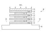
Si + 2GeF4 → SiF4↑ + 2GeF2↑ …(1)
(1)式の反応は、上記他の物質に対してはほとんど生じず、したがって、Siのみが選択的にエッチングされるものと考えられる。他の物質がSiGeの場合はSiが含まれているものの、Geにより保護されてGeF4ガスではほとんどエッチングされない。SiO2、SiNもSiが酸素または窒素と強固に結合しているため、同様にほとんどエッチングされない。また、他の物質がGeの場合は、Siが含まれておらず、GeはGeF4とは反応しないため、さらにエッチングされ難い。
次に、一実施形態に係るエッチング方法に用いる処理システムの一例について説明する。図8は、処理システムの一例を示す概略構成図である。
次に、一実施形態に係るエッチング方法を実施するためのエッチング装置105の一例について詳細に説明する。
図9はエッチング装置105の一例を示す断面図である。図9に示すように、エッチング装置105は、処理空間を規定する処理容器としての密閉構造のチャンバー140を備えており、チャンバー140の内部には、ウエハWを略水平にした状態で載置させる載置台142が設けられている。また、エッチング装置105は、チャンバー140にエッチングガスを供給するガス供給部143、チャンバー140内を排気する排気部144を備えている。
次に、実験例について説明する。
ここでは、ベアウエハにそれぞれSi膜、SiGe膜(Ge30at%)、熱酸化膜(ThOx膜)(SiO2膜)、SiN膜、Ge膜を形成したサンプルを準備し、GeF4ガスによりエッチングを行った。エッチング後の重量変化から換算してエッチングレートを求めた。エッチング条件としては、エッチングが進行しやすい以下の条件とした。
ガス:100%-GeF4
ガス流量:10~50sccm
圧力:50~150Torr
処理温度(ウエハ温度):25~300℃
以上、実施形態について説明したが、今回開示された実施形態は、全ての点で例示であって制限的なものではないと考えられるべきである。上記の実施形態は、添付の特許請求の範囲およびその主旨を逸脱することなく、様々な形態で省略、置換、変更されてもよい。
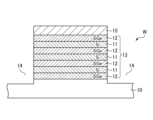
11;Si膜
12;SiGe膜
13;積層構造部
14;凹部
15;マスク層
100;処理システム
105;エッチング装置
142;載置台
143;処理ガス供給部
144;排気部
165;温度調節器
W;半導体ウエハ(基板)
Claims (17)
- Siと、SiGe、Ge、SiO 2 、SiNから選択される少なくとも一種からなる他の物質とを有する基板を設ける工程と、
前記基板にゲルマニウム化合物ガスからなるエッチングガスのみ、または、ゲルマニウム化合物ガスからなるエッチングガスと不活性ガスとを供給し、前記Siを前記他の物質に対して選択的にエッチングする工程と、
を有する、エッチング方法。 - 前記ゲルマニウム化合物ガスは、ゲルマニウムと水素またはハロゲンとの化合物ガスである、請求項1に記載のエッチング方法。
- 前記ゲルマニウムと水素またはハロゲンとの化合物ガスは、GeF4ガス、GeF2Cl2ガス、GeCl4ガス、GeH4ガスの少なくとも一種である、請求項2に記載のエッチング方法。
- 前記他の物質はSiGeまたはGeである、請求項1から請求項3のいずれか一項に記載のエッチング方法。
- 前記SiがSi膜であり、前記SiGeまたはGeが、SiGe膜またはGe膜である、請求項4に記載のエッチング方法。
- 前記SiGe膜、前記Ge膜、および前記Si膜は、エピタキシャル法により形成されたものである、請求項5に記載のエッチング方法。
- 前記基板は、前記Si膜と前記SiGe膜または前記Ge膜とが交互に積層されてなる積層構造部を有する、請求項5または請求項6に記載のエッチング方法。
- 前記エッチングする工程における圧力は、1.33~39990Paの範囲である、請求項1から請求項7のいずれか一項に記載のエッチング方法。
- 前記エッチングする工程における基板の温度は、-20℃以上、300℃以下である、請求項1から請求項8いずれか一項に記載のエッチング方法。
- 前記エッチングする工程における基板の温度は、150℃以下である、請求項9に記載のエッチング方法。
- 前記エッチングする工程に先立って行われる、基板の表面の自然酸化膜を除去する工程をさらに有する、請求項1から請求項10のいずれか一項に記載のエッチング方法。
- 前記エッチングする工程の後に残存する残存物を除去する工程をさらに有する、請求項1から請求項11のいずれか一項に記載のエッチング方法。
- 前記エッチングする工程は、前記エッチングガス、または前記エッチングガスと前記不活性ガスとをプラズマ化せずに前記基板に供給するノンプラズマエッチングにより行う、請求項1から請求項12のいずれか1項に記載のエッチング方法。
- Siと、SiGe、Ge、SiO 2 、SiNから選択される少なくとも一種からなる他の物質とを有する基板を収容するチャンバーと、
前記チャンバー内で前記基板を載置する載置台と、
前記チャンバー内にゲルマニウム化合物ガスからなるエッチングガスのみ、または、ゲルマニウム化合物ガスからなるエッチングガスと不活性ガスとを供給するガス供給部と、
前記チャンバー内を排気する排気部と、
前記載置台上の基板の温度を調節する温調部と、
制御部と、
を具備し、
前記制御部は、前記基板にゲルマニウム化合物ガスからなるエッチングガスのみ、または、ゲルマニウム化合物ガスからなるエッチングガスと不活性ガスとが供給され、前記Siが前記他の物質に対して選択的にエッチングされるように、前記ガス供給部と、前記排気部と、前記温調部とを制御する、エッチング装置。 - 前記ゲルマニウム化合物ガスは、ゲルマニウムと水素またはハロゲンとの化合物ガスである、請求項14に記載のエッチング装置。
- 前記ゲルマニウムと水素またはハロゲンとの化合物ガスは、GeF4ガス、GeF2Cl2ガス、GeCl4ガス、GeH4ガスの少なくとも一種である、請求項15に記載のエッチング装置。
- 前記他の物質はSiGeまたはGeである、請求項14から請求項16のいずれか一項に記載のエッチング装置。
Priority Applications (4)
| Application Number | Priority Date | Filing Date | Title |
|---|---|---|---|
| JP2019111110A JP7313201B2 (ja) | 2019-06-14 | 2019-06-14 | エッチング方法およびエッチング装置 |
| KR1020200066308A KR102944091B1 (ko) | 2019-06-14 | 2020-06-02 | 에칭 방법 및 에칭 장치 |
| TW109118417A TWI850393B (zh) | 2019-06-14 | 2020-06-02 | 蝕刻方法及蝕刻裝置 |
| US16/900,227 US11594417B2 (en) | 2019-06-14 | 2020-06-12 | Etching method and apparatus |
Applications Claiming Priority (1)
| Application Number | Priority Date | Filing Date | Title |
|---|---|---|---|
| JP2019111110A JP7313201B2 (ja) | 2019-06-14 | 2019-06-14 | エッチング方法およびエッチング装置 |
Publications (2)
| Publication Number | Publication Date |
|---|---|
| JP2020205304A JP2020205304A (ja) | 2020-12-24 |
| JP7313201B2 true JP7313201B2 (ja) | 2023-07-24 |
Family
ID=73745653
Family Applications (1)
| Application Number | Title | Priority Date | Filing Date |
|---|---|---|---|
| JP2019111110A Active JP7313201B2 (ja) | 2019-06-14 | 2019-06-14 | エッチング方法およびエッチング装置 |
Country Status (4)
| Country | Link |
|---|---|
| US (1) | US11594417B2 (ja) |
| JP (1) | JP7313201B2 (ja) |
| KR (1) | KR102944091B1 (ja) |
| TW (1) | TWI850393B (ja) |
Families Citing this family (9)
| Publication number | Priority date | Publication date | Assignee | Title |
|---|---|---|---|---|
| JP7673397B2 (ja) * | 2020-12-10 | 2025-05-09 | 株式会社三洋物産 | 遊技機 |
| JP7673396B2 (ja) * | 2020-12-10 | 2025-05-09 | 株式会社三洋物産 | 遊技機 |
| JP7673398B2 (ja) * | 2020-12-10 | 2025-05-09 | 株式会社三洋物産 | 遊技機 |
| JP7771835B2 (ja) * | 2021-05-31 | 2025-11-18 | 東京エレクトロン株式会社 | 基板処理方法及び基板処理装置 |
| JP7497719B2 (ja) * | 2021-12-16 | 2024-06-11 | 株式会社三洋物産 | 遊技機 |
| JP7497720B2 (ja) * | 2021-12-16 | 2024-06-11 | 株式会社三洋物産 | 遊技機 |
| JP7497718B2 (ja) * | 2021-12-16 | 2024-06-11 | 株式会社三洋物産 | 遊技機 |
| JP7831210B2 (ja) * | 2022-09-21 | 2026-03-17 | 東京エレクトロン株式会社 | 基板処理方法及び基板処理装置 |
| US20250201570A1 (en) * | 2023-06-01 | 2025-06-19 | Hitachi High-Tech Corporation | Wafer processing method and wafer processing system |
Citations (2)
| Publication number | Priority date | Publication date | Assignee | Title |
|---|---|---|---|---|
| JP2013225604A (ja) | 2012-04-23 | 2013-10-31 | Hitachi High-Technologies Corp | ドライエッチング方法 |
| JP2016143781A (ja) | 2015-02-03 | 2016-08-08 | 東京エレクトロン株式会社 | エッチング方法 |
Family Cites Families (13)
| Publication number | Priority date | Publication date | Assignee | Title |
|---|---|---|---|---|
| US5342805A (en) * | 1993-07-01 | 1994-08-30 | G.I. Corporation | Method of growing a semiconductor material by epilaxy |
| DE102005047081B4 (de) | 2005-09-30 | 2019-01-31 | Robert Bosch Gmbh | Verfahren zum plasmalosen Ätzen von Silizium mit dem Ätzgas ClF3 oder XeF2 |
| US8278176B2 (en) * | 2006-06-07 | 2012-10-02 | Asm America, Inc. | Selective epitaxial formation of semiconductor films |
| US8778767B2 (en) * | 2010-11-18 | 2014-07-15 | Taiwan Semiconductor Manufacturing Company, Ltd. | Integrated circuits and fabrication methods thereof |
| KR20120108338A (ko) * | 2011-03-23 | 2012-10-05 | 삼성전자주식회사 | 반도체 소자의 제조방법 |
| US20130025538A1 (en) * | 2011-07-27 | 2013-01-31 | Applied Materials, Inc. | Methods and apparatus for deposition processes |
| JP2014060391A (ja) * | 2012-08-24 | 2014-04-03 | Sumitomo Chemical Co Ltd | 半導体基板の製造方法、半導体基板、半導体装置の製造方法および半導体装置 |
| US9093468B2 (en) * | 2013-03-13 | 2015-07-28 | Taiwan Semiconductor Manufacturing Company, Ltd. | Asymmetric cyclic depositon and etch process for epitaxial formation mechanisms of source and drain regions |
| US8940595B2 (en) * | 2013-03-15 | 2015-01-27 | International Business Machines Corporation | Faceted intrinsic epitaxial buffer layer for reducing short channel effects while maximizing channel stress levels |
| US8927431B2 (en) * | 2013-05-31 | 2015-01-06 | International Business Machines Corporation | High-rate chemical vapor etch of silicon substrates |
| US10665693B2 (en) * | 2015-04-30 | 2020-05-26 | Taiwan Semiconductor Manufacturing Co., Ltd. | Semiconductor structure and manufacturing method thereof |
| JP2017092142A (ja) * | 2015-11-05 | 2017-05-25 | 東京エレクトロン株式会社 | 被処理体を処理する方法 |
| US10325820B1 (en) * | 2018-01-10 | 2019-06-18 | International Business Machines Corporation | Source and drain isolation for CMOS nanosheet with one block mask |
-
2019
- 2019-06-14 JP JP2019111110A patent/JP7313201B2/ja active Active
-
2020
- 2020-06-02 KR KR1020200066308A patent/KR102944091B1/ko active Active
- 2020-06-02 TW TW109118417A patent/TWI850393B/zh active
- 2020-06-12 US US16/900,227 patent/US11594417B2/en active Active
Patent Citations (2)
| Publication number | Priority date | Publication date | Assignee | Title |
|---|---|---|---|---|
| JP2013225604A (ja) | 2012-04-23 | 2013-10-31 | Hitachi High-Technologies Corp | ドライエッチング方法 |
| JP2016143781A (ja) | 2015-02-03 | 2016-08-08 | 東京エレクトロン株式会社 | エッチング方法 |
Also Published As
| Publication number | Publication date |
|---|---|
| KR20200143260A (ko) | 2020-12-23 |
| KR102944091B1 (ko) | 2026-03-25 |
| JP2020205304A (ja) | 2020-12-24 |
| US20200395219A1 (en) | 2020-12-17 |
| TW202113966A (zh) | 2021-04-01 |
| US11594417B2 (en) | 2023-02-28 |
| TWI850393B (zh) | 2024-08-01 |
Similar Documents
| Publication | Publication Date | Title |
|---|---|---|
| JP7313201B2 (ja) | エッチング方法およびエッチング装置 | |
| JP7113711B2 (ja) | エッチング方法、エッチング装置、および記憶媒体 | |
| JP7204348B2 (ja) | エッチング方法およびエッチング装置 | |
| KR102181910B1 (ko) | 에칭 방법 및 잔사 제거 방법 | |
| KR101790406B1 (ko) | 에칭 방법 및 기억 매체 | |
| JP7109165B2 (ja) | エッチング方法 | |
| KR101802580B1 (ko) | 에칭 방법 및 기억 매체 | |
| US11011383B2 (en) | Etching method | |
| TW201701348A (zh) | 蝕刻方法 | |
| JP6097192B2 (ja) | エッチング方法 | |
| JP6073172B2 (ja) | エッチング方法 | |
| JP2014236055A (ja) | エッチング方法 | |
| WO2016056401A1 (ja) | エッチング方法 | |
| JP7145740B2 (ja) | エッチング方法 | |
| WO2015186461A1 (ja) | エッチング方法 | |
| JP2015073035A (ja) | エッチング方法 |
Legal Events
| Date | Code | Title | Description |
|---|---|---|---|
| A621 | Written request for application examination |
Free format text: JAPANESE INTERMEDIATE CODE: A621 Effective date: 20220413 |
|
| A977 | Report on retrieval |
Free format text: JAPANESE INTERMEDIATE CODE: A971007 Effective date: 20230119 |
|
| A131 | Notification of reasons for refusal |
Free format text: JAPANESE INTERMEDIATE CODE: A131 Effective date: 20230124 |
|
| A521 | Request for written amendment filed |
Free format text: JAPANESE INTERMEDIATE CODE: A523 Effective date: 20230303 |
|
| A131 | Notification of reasons for refusal |
Free format text: JAPANESE INTERMEDIATE CODE: A131 Effective date: 20230411 |
|
| A521 | Request for written amendment filed |
Free format text: JAPANESE INTERMEDIATE CODE: A523 Effective date: 20230608 |
|
| TRDD | Decision of grant or rejection written | ||
| A01 | Written decision to grant a patent or to grant a registration (utility model) |
Free format text: JAPANESE INTERMEDIATE CODE: A01 Effective date: 20230613 |
|
| A61 | First payment of annual fees (during grant procedure) |
Free format text: JAPANESE INTERMEDIATE CODE: A61 Effective date: 20230711 |
|
| R150 | Certificate of patent or registration of utility model |
Ref document number: 7313201 Country of ref document: JP Free format text: JAPANESE INTERMEDIATE CODE: R150 |