JP7315523B2 - 端子の固着方法 - Google Patents
端子の固着方法 Download PDFInfo
- Publication number
- JP7315523B2 JP7315523B2 JP2020201601A JP2020201601A JP7315523B2 JP 7315523 B2 JP7315523 B2 JP 7315523B2 JP 2020201601 A JP2020201601 A JP 2020201601A JP 2020201601 A JP2020201601 A JP 2020201601A JP 7315523 B2 JP7315523 B2 JP 7315523B2
- Authority
- JP
- Japan
- Prior art keywords
- lands
- land
- dummy
- terminal
- fpc
- Prior art date
- Legal status (The legal status is an assumption and is not a legal conclusion. Google has not performed a legal analysis and makes no representation as to the accuracy of the status listed.)
- Active
Links
Images


Classifications
-
- H—ELECTRICITY
- H01—ELECTRIC ELEMENTS
- H01R—ELECTRICALLY-CONDUCTIVE CONNECTIONS; STRUCTURAL ASSOCIATIONS OF A PLURALITY OF MUTUALLY-INSULATED ELECTRICAL CONNECTING ELEMENTS; COUPLING DEVICES; CURRENT COLLECTORS
- H01R43/00—Apparatus or processes specially adapted for manufacturing, assembling, maintaining, or repairing of line connectors or current collectors or for joining electric conductors
- H01R43/02—Apparatus or processes specially adapted for manufacturing, assembling, maintaining, or repairing of line connectors or current collectors or for joining electric conductors for soldered or welded connections
- H01R43/0256—Apparatus or processes specially adapted for manufacturing, assembling, maintaining, or repairing of line connectors or current collectors or for joining electric conductors for soldered or welded connections for soldering or welding connectors to a printed circuit board
-
- H—ELECTRICITY
- H01—ELECTRIC ELEMENTS
- H01R—ELECTRICALLY-CONDUCTIVE CONNECTIONS; STRUCTURAL ASSOCIATIONS OF A PLURALITY OF MUTUALLY-INSULATED ELECTRICAL CONNECTING ELEMENTS; COUPLING DEVICES; CURRENT COLLECTORS
- H01R43/00—Apparatus or processes specially adapted for manufacturing, assembling, maintaining, or repairing of line connectors or current collectors or for joining electric conductors
- H01R43/02—Apparatus or processes specially adapted for manufacturing, assembling, maintaining, or repairing of line connectors or current collectors or for joining electric conductors for soldered or welded connections
- H01R43/0221—Laser welding
-
- B—PERFORMING OPERATIONS; TRANSPORTING
- B23—MACHINE TOOLS; METAL-WORKING NOT OTHERWISE PROVIDED FOR
- B23K—SOLDERING OR UNSOLDERING; WELDING; CLADDING OR PLATING BY SOLDERING OR WELDING; CUTTING BY APPLYING HEAT LOCALLY, e.g. FLAME CUTTING; WORKING BY LASER BEAM
- B23K1/00—Soldering, e.g. brazing, or unsoldering
- B23K1/0008—Soldering, e.g. brazing, or unsoldering specially adapted for particular articles or work
- B23K1/0016—Soldering of electronic components
-
- B—PERFORMING OPERATIONS; TRANSPORTING
- B23—MACHINE TOOLS; METAL-WORKING NOT OTHERWISE PROVIDED FOR
- B23K—SOLDERING OR UNSOLDERING; WELDING; CLADDING OR PLATING BY SOLDERING OR WELDING; CUTTING BY APPLYING HEAT LOCALLY, e.g. FLAME CUTTING; WORKING BY LASER BEAM
- B23K1/00—Soldering, e.g. brazing, or unsoldering
- B23K1/005—Soldering by means of radiant energy
- B23K1/0056—Soldering by means of radiant energy soldering by means of beams, e.g. lasers, electron beams [EB]
-
- B—PERFORMING OPERATIONS; TRANSPORTING
- B23—MACHINE TOOLS; METAL-WORKING NOT OTHERWISE PROVIDED FOR
- B23K—SOLDERING OR UNSOLDERING; WELDING; CLADDING OR PLATING BY SOLDERING OR WELDING; CUTTING BY APPLYING HEAT LOCALLY, e.g. FLAME CUTTING; WORKING BY LASER BEAM
- B23K26/00—Working by laser beam, e.g. welding, cutting or boring
- B23K26/009—Working by laser beam, e.g. welding, cutting or boring using a non-absorbing, e.g. transparent, reflective or refractive, layer on the workpiece
-
- B—PERFORMING OPERATIONS; TRANSPORTING
- B23—MACHINE TOOLS; METAL-WORKING NOT OTHERWISE PROVIDED FOR
- B23K—SOLDERING OR UNSOLDERING; WELDING; CLADDING OR PLATING BY SOLDERING OR WELDING; CUTTING BY APPLYING HEAT LOCALLY, e.g. FLAME CUTTING; WORKING BY LASER BEAM
- B23K26/00—Working by laser beam, e.g. welding, cutting or boring
- B23K26/02—Positioning or observing the workpiece, e.g. with respect to the point of impact; Aligning, aiming or focusing the laser beam
- B23K26/06—Shaping the laser beam, e.g. by masks or multi-focusing
- B23K26/067—Dividing the beam into multiple beams, e.g. multi-focusing
-
- H—ELECTRICITY
- H01—ELECTRIC ELEMENTS
- H01R—ELECTRICALLY-CONDUCTIVE CONNECTIONS; STRUCTURAL ASSOCIATIONS OF A PLURALITY OF MUTUALLY-INSULATED ELECTRICAL CONNECTING ELEMENTS; COUPLING DEVICES; CURRENT COLLECTORS
- H01R43/00—Apparatus or processes specially adapted for manufacturing, assembling, maintaining, or repairing of line connectors or current collectors or for joining electric conductors
- H01R43/02—Apparatus or processes specially adapted for manufacturing, assembling, maintaining, or repairing of line connectors or current collectors or for joining electric conductors for soldered or welded connections
- H01R43/0249—Apparatus or processes specially adapted for manufacturing, assembling, maintaining, or repairing of line connectors or current collectors or for joining electric conductors for soldered or welded connections for simultaneous welding or soldering of a plurality of wires to contact elements
-
- H—ELECTRICITY
- H05—ELECTRIC TECHNIQUES NOT OTHERWISE PROVIDED FOR
- H05K—PRINTED CIRCUITS; CASINGS OR CONSTRUCTIONAL DETAILS OF ELECTRIC APPARATUS; MANUFACTURE OF ASSEMBLAGES OF ELECTRICAL COMPONENTS
- H05K3/00—Apparatus or processes for manufacturing printed circuits
- H05K3/30—Assembling printed circuits with electric components, e.g. with resistors
- H05K3/32—Assembling printed circuits with electric components, e.g. with resistors electrically connecting electric components or wires to printed circuits
- H05K3/34—Assembling printed circuits with electric components, e.g. with resistors electrically connecting electric components or wires to printed circuits by soldering
- H05K3/3447—Lead-in-hole components
-
- H—ELECTRICITY
- H05—ELECTRIC TECHNIQUES NOT OTHERWISE PROVIDED FOR
- H05K—PRINTED CIRCUITS; CASINGS OR CONSTRUCTIONAL DETAILS OF ELECTRIC APPARATUS; MANUFACTURE OF ASSEMBLAGES OF ELECTRICAL COMPONENTS
- H05K3/00—Apparatus or processes for manufacturing printed circuits
- H05K3/30—Assembling printed circuits with electric components, e.g. with resistors
- H05K3/32—Assembling printed circuits with electric components, e.g. with resistors electrically connecting electric components or wires to printed circuits
- H05K3/34—Assembling printed circuits with electric components, e.g. with resistors electrically connecting electric components or wires to printed circuits by soldering
- H05K3/3494—Heating processes for reflow soldering
-
- B—PERFORMING OPERATIONS; TRANSPORTING
- B23—MACHINE TOOLS; METAL-WORKING NOT OTHERWISE PROVIDED FOR
- B23K—SOLDERING OR UNSOLDERING; WELDING; CLADDING OR PLATING BY SOLDERING OR WELDING; CUTTING BY APPLYING HEAT LOCALLY, e.g. FLAME CUTTING; WORKING BY LASER BEAM
- B23K2101/00—Articles made by soldering, welding or cutting
- B23K2101/36—Electric or electronic devices
- B23K2101/38—Conductors
-
- B—PERFORMING OPERATIONS; TRANSPORTING
- B23—MACHINE TOOLS; METAL-WORKING NOT OTHERWISE PROVIDED FOR
- B23K—SOLDERING OR UNSOLDERING; WELDING; CLADDING OR PLATING BY SOLDERING OR WELDING; CUTTING BY APPLYING HEAT LOCALLY, e.g. FLAME CUTTING; WORKING BY LASER BEAM
- B23K2101/00—Articles made by soldering, welding or cutting
- B23K2101/36—Electric or electronic devices
- B23K2101/42—Printed circuits
-
- H—ELECTRICITY
- H01—ELECTRIC ELEMENTS
- H01R—ELECTRICALLY-CONDUCTIVE CONNECTIONS; STRUCTURAL ASSOCIATIONS OF A PLURALITY OF MUTUALLY-INSULATED ELECTRICAL CONNECTING ELEMENTS; COUPLING DEVICES; CURRENT COLLECTORS
- H01R12/00—Structural associations of a plurality of mutually-insulated electrical connecting elements, specially adapted for printed circuits, e.g. printed circuit boards [PCB], flat or ribbon cables, or like generally planar structures, e.g. terminal strips, terminal blocks; Coupling devices specially adapted for printed circuits, flat or ribbon cables, or like generally planar structures; Terminals specially adapted for contact with, or insertion into, printed circuits, flat or ribbon cables, or like generally planar structures
- H01R12/50—Fixed connections
- H01R12/51—Fixed connections for rigid printed circuits or like structures
- H01R12/55—Fixed connections for rigid printed circuits or like structures characterised by the terminals
- H01R12/58—Fixed connections for rigid printed circuits or like structures characterised by the terminals terminals for insertion into holes
-
- H—ELECTRICITY
- H01—ELECTRIC ELEMENTS
- H01R—ELECTRICALLY-CONDUCTIVE CONNECTIONS; STRUCTURAL ASSOCIATIONS OF A PLURALITY OF MUTUALLY-INSULATED ELECTRICAL CONNECTING ELEMENTS; COUPLING DEVICES; CURRENT COLLECTORS
- H01R12/00—Structural associations of a plurality of mutually-insulated electrical connecting elements, specially adapted for printed circuits, e.g. printed circuit boards [PCB], flat or ribbon cables, or like generally planar structures, e.g. terminal strips, terminal blocks; Coupling devices specially adapted for printed circuits, flat or ribbon cables, or like generally planar structures; Terminals specially adapted for contact with, or insertion into, printed circuits, flat or ribbon cables, or like generally planar structures
- H01R12/50—Fixed connections
- H01R12/59—Fixed connections for flexible printed circuits, flat or ribbon cables or like structures
- H01R12/65—Fixed connections for flexible printed circuits, flat or ribbon cables or like structures characterised by the terminal
- H01R12/67—Fixed connections for flexible printed circuits, flat or ribbon cables or like structures characterised by the terminal insulation penetrating terminals
-
- H—ELECTRICITY
- H05—ELECTRIC TECHNIQUES NOT OTHERWISE PROVIDED FOR
- H05K—PRINTED CIRCUITS; CASINGS OR CONSTRUCTIONAL DETAILS OF ELECTRIC APPARATUS; MANUFACTURE OF ASSEMBLAGES OF ELECTRICAL COMPONENTS
- H05K1/00—Printed circuits
- H05K1/02—Details
- H05K1/03—Use of materials for the substrate
- H05K1/0393—Flexible materials
-
- H—ELECTRICITY
- H05—ELECTRIC TECHNIQUES NOT OTHERWISE PROVIDED FOR
- H05K—PRINTED CIRCUITS; CASINGS OR CONSTRUCTIONAL DETAILS OF ELECTRIC APPARATUS; MANUFACTURE OF ASSEMBLAGES OF ELECTRICAL COMPONENTS
- H05K1/00—Printed circuits
- H05K1/02—Details
- H05K1/11—Printed elements for providing electric connections to or between printed circuits
- H05K1/118—Printed elements for providing electric connections to or between printed circuits specially for flexible printed circuits, e.g. using folded portions
-
- H—ELECTRICITY
- H05—ELECTRIC TECHNIQUES NOT OTHERWISE PROVIDED FOR
- H05K—PRINTED CIRCUITS; CASINGS OR CONSTRUCTIONAL DETAILS OF ELECTRIC APPARATUS; MANUFACTURE OF ASSEMBLAGES OF ELECTRICAL COMPONENTS
- H05K2201/00—Indexing scheme relating to printed circuits covered by H05K1/00
- H05K2201/09—Shape and layout
- H05K2201/09209—Shape and layout details of conductors
- H05K2201/09372—Pads and lands
- H05K2201/094—Array of pads or lands differing from one another, e.g. in size, pitch or thickness; Using different connections on the pads
-
- H—ELECTRICITY
- H05—ELECTRIC TECHNIQUES NOT OTHERWISE PROVIDED FOR
- H05K—PRINTED CIRCUITS; CASINGS OR CONSTRUCTIONAL DETAILS OF ELECTRIC APPARATUS; MANUFACTURE OF ASSEMBLAGES OF ELECTRICAL COMPONENTS
- H05K2201/00—Indexing scheme relating to printed circuits covered by H05K1/00
- H05K2201/09—Shape and layout
- H05K2201/09209—Shape and layout details of conductors
- H05K2201/09372—Pads and lands
- H05K2201/09409—Multiple rows of pads, lands, terminals or dummy patterns; Multiple rows of mounted components
-
- H—ELECTRICITY
- H05—ELECTRIC TECHNIQUES NOT OTHERWISE PROVIDED FOR
- H05K—PRINTED CIRCUITS; CASINGS OR CONSTRUCTIONAL DETAILS OF ELECTRIC APPARATUS; MANUFACTURE OF ASSEMBLAGES OF ELECTRICAL COMPONENTS
- H05K2201/00—Indexing scheme relating to printed circuits covered by H05K1/00
- H05K2201/09—Shape and layout
- H05K2201/09209—Shape and layout details of conductors
- H05K2201/09654—Shape and layout details of conductors covering at least two types of conductors provided for in H05K2201/09218 - H05K2201/095
- H05K2201/09781—Dummy conductors, i.e. not used for normal transport of current; Dummy electrodes of components
-
- H—ELECTRICITY
- H05—ELECTRIC TECHNIQUES NOT OTHERWISE PROVIDED FOR
- H05K—PRINTED CIRCUITS; CASINGS OR CONSTRUCTIONAL DETAILS OF ELECTRIC APPARATUS; MANUFACTURE OF ASSEMBLAGES OF ELECTRICAL COMPONENTS
- H05K2201/00—Indexing scheme relating to printed circuits covered by H05K1/00
- H05K2201/10—Details of components or other objects attached to or integrated in a printed circuit board
- H05K2201/10227—Other objects, e.g. metallic pieces
- H05K2201/10295—Metallic connector elements partly mounted in a hole of the PCB
- H05K2201/10303—Pin-in-hole mounted pins
-
- H—ELECTRICITY
- H05—ELECTRIC TECHNIQUES NOT OTHERWISE PROVIDED FOR
- H05K—PRINTED CIRCUITS; CASINGS OR CONSTRUCTIONAL DETAILS OF ELECTRIC APPARATUS; MANUFACTURE OF ASSEMBLAGES OF ELECTRICAL COMPONENTS
- H05K2203/00—Indexing scheme relating to apparatus or processes for manufacturing printed circuits covered by H05K3/00
- H05K2203/10—Using electric, magnetic and electromagnetic fields; Using laser light
- H05K2203/107—Using laser light
-
- H—ELECTRICITY
- H05—ELECTRIC TECHNIQUES NOT OTHERWISE PROVIDED FOR
- H05K—PRINTED CIRCUITS; CASINGS OR CONSTRUCTIONAL DETAILS OF ELECTRIC APPARATUS; MANUFACTURE OF ASSEMBLAGES OF ELECTRICAL COMPONENTS
- H05K5/00—Casings, cabinets or drawers for electric apparatus
- H05K5/0026—Casings, cabinets or drawers for electric apparatus provided with connectors and printed circuit boards [PCB], e.g. automotive electronic control units
- H05K5/0069—Casings, cabinets or drawers for electric apparatus provided with connectors and printed circuit boards [PCB], e.g. automotive electronic control units having connector relating features for connecting the connector pins with the PCB or for mounting the connector body with the housing
Landscapes
- Engineering & Computer Science (AREA)
- Physics & Mathematics (AREA)
- Optics & Photonics (AREA)
- Manufacturing & Machinery (AREA)
- Mechanical Engineering (AREA)
- Plasma & Fusion (AREA)
- Microelectronics & Electronic Packaging (AREA)
- Electric Connection Of Electric Components To Printed Circuits (AREA)
- Manufacturing Of Electrical Connectors (AREA)
- Printing Elements For Providing Electric Connections Between Printed Circuits (AREA)
- Combinations Of Printed Boards (AREA)
Description
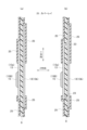
3 端子(コネクタ端子)
9 基板(FPC)
11 端子設置用ランド
13 ダミーランド
13a 表面ダミーランド
13b 裏面ダミーランド
15 ろう(ハンダ)
19、19A、19B レーザ光(分割レーザ光)
25 カバーレイ
Claims (5)
- 基板に設けられている複数のランドのそれぞれに、レーザ溶接によって端子を固着させる端子の固着方法であって、
前記複数のランドは、前記端子が設置される端子設置用ランドと、前記端子設置用ランドよりも大きいダミーランドとで成り立っており、
前記レーザ溶接では、レーザ発振器から出射され複数に分けられたレーザ光のそれぞれを、前記複数のランドのうちの一部の複数のランドのそれぞれに向けて照射するようになっており、
前記一部の複数のランドが前記端子設置用ランドで成り立っているか、もしくは、前記一部の複数のランドが前記端子設置用ランドと前記ダミーランドとで成り立っており、
前記ダミーランドは、前記基板の厚さ方向の一方の面である表面に設けられている表面ダミーランドと、前記基板の厚さ方向の他方の面である裏面に設けられている裏面ダミーランドとで成り立っていて、前記表面ダミーランドと前記裏面ダミーランドとは、前記基板を貫通している連結部によってお互いがつながっている端子の固着方法。 - 前記表面ダミーランドの面積と前記裏面ダミーランドの面積とは、お互いが異なっている請求項1に記載の端子の固着方法。
- 前記レーザ溶接では、前記ダミーランドにろうを配置しておき、前記ダミーランドに向けて前記レーザ光を照射する請求項1または請求項2に記載の端子の固着方法。
- 前記ダミーランドの少なくとも一部が、前記基板に設けられているカバーレイで覆われている請求項1~請求項3のいずれか1項に記載の端子の固着方法。
- 前記基板がFPCである請求項1~請求項4のいずれか1項に記載の端子の固着方法。
Priority Applications (4)
| Application Number | Priority Date | Filing Date | Title |
|---|---|---|---|
| JP2020201601A JP7315523B2 (ja) | 2020-12-04 | 2020-12-04 | 端子の固着方法 |
| EP21211663.6A EP4008469B1 (en) | 2020-12-04 | 2021-12-01 | Terminal fixing method |
| US17/541,005 US12592533B2 (en) | 2020-12-04 | 2021-12-02 | Terminal fixing method |
| CN202111460088.1A CN114597727B (zh) | 2020-12-04 | 2021-12-02 | 端子固定方法 |
Applications Claiming Priority (1)
| Application Number | Priority Date | Filing Date | Title |
|---|---|---|---|
| JP2020201601A JP7315523B2 (ja) | 2020-12-04 | 2020-12-04 | 端子の固着方法 |
Publications (2)
| Publication Number | Publication Date |
|---|---|
| JP2022089301A JP2022089301A (ja) | 2022-06-16 |
| JP7315523B2 true JP7315523B2 (ja) | 2023-07-26 |
Family
ID=78820298
Family Applications (1)
| Application Number | Title | Priority Date | Filing Date |
|---|---|---|---|
| JP2020201601A Active JP7315523B2 (ja) | 2020-12-04 | 2020-12-04 | 端子の固着方法 |
Country Status (4)
| Country | Link |
|---|---|
| US (1) | US12592533B2 (ja) |
| EP (1) | EP4008469B1 (ja) |
| JP (1) | JP7315523B2 (ja) |
| CN (1) | CN114597727B (ja) |
Families Citing this family (2)
| Publication number | Priority date | Publication date | Assignee | Title |
|---|---|---|---|---|
| CN117500180A (zh) * | 2022-07-26 | 2024-02-02 | 京东方科技集团股份有限公司 | 一种焊盘修复设备及焊盘修复方法 |
| JP2025030373A (ja) | 2023-08-23 | 2025-03-07 | 矢崎総業株式会社 | 回路体、及び、コネクタ付き回路体 |
Citations (1)
| Publication number | Priority date | Publication date | Assignee | Title |
|---|---|---|---|---|
| JP2003069163A (ja) | 2001-08-22 | 2003-03-07 | Olympus Optical Co Ltd | フレキシブルプリント基板 |
Family Cites Families (21)
| Publication number | Priority date | Publication date | Assignee | Title |
|---|---|---|---|---|
| US3586813A (en) * | 1967-08-31 | 1971-06-22 | Western Electric Co | Simultaneous multiple lead bonding |
| JPS62104194A (ja) * | 1985-10-31 | 1987-05-14 | キヤノン株式会社 | レ−ザ半田付け用両面プリント配線板 |
| DE3831743A1 (de) | 1988-09-17 | 1990-03-29 | Philips Patentverwaltung | Vorrichtung zur bearbeitung eines werkstueckes mit laserlicht und verwendung dieser vorrichtung |
| JPH0521515A (ja) * | 1991-07-15 | 1993-01-29 | Seiko Epson Corp | 液晶表示デバイスとその製造方法 |
| US5495089A (en) * | 1993-06-04 | 1996-02-27 | Digital Equipment Corporation | Laser soldering surface mount components of a printed circuit board |
| JP3395621B2 (ja) * | 1997-02-03 | 2003-04-14 | イビデン株式会社 | プリント配線板及びその製造方法 |
| JPH10335806A (ja) * | 1997-04-04 | 1998-12-18 | Taiyo Yuden Co Ltd | 回路モジュールの製造方法及びその装置 |
| US6333483B1 (en) * | 1997-04-04 | 2001-12-25 | Taiyo Yuden Co., Ltd. | Method of manufacturing circuit modules |
| JP2005050603A (ja) | 2003-07-31 | 2005-02-24 | Yazaki Corp | 端子固定方法 |
| JP5292665B2 (ja) * | 2005-10-31 | 2013-09-18 | 株式会社ジャパンディスプレイ | 表示装置 |
| JP2007265962A (ja) | 2006-02-28 | 2007-10-11 | Hitachi Ltd | レーザ溶接方法,コントロールユニットの製造方法、及び車両用コントロールユニット |
| US7677905B2 (en) * | 2006-12-13 | 2010-03-16 | Denso Corporation | Electronic device and manufacturing method of the same |
| JP2009019975A (ja) * | 2007-07-11 | 2009-01-29 | Micronics Japan Co Ltd | プローブ組立体およびその製造方法 |
| KR100912037B1 (ko) * | 2007-12-03 | 2009-08-12 | (주)엘지하우시스 | 태양전지 모듈의 제조 방법 및 제조 장치 |
| JP4433058B2 (ja) * | 2008-01-30 | 2010-03-17 | 株式会社デンソー | 電子装置及びその製造方法 |
| JP5535408B1 (ja) | 2012-07-09 | 2014-07-02 | 古河電気工業株式会社 | 圧着端子、接続構造体及びコネクタ |
| JP6329027B2 (ja) * | 2014-08-04 | 2018-05-23 | ミネベアミツミ株式会社 | フレキシブルプリント基板 |
| JP6392630B2 (ja) * | 2014-10-28 | 2018-09-19 | 京セラ株式会社 | 回路基板および回路装置 |
| JP6390354B2 (ja) | 2014-11-06 | 2018-09-19 | オムロン株式会社 | 端子固定装置および端子固定方法 |
| JP2017010984A (ja) * | 2015-06-17 | 2017-01-12 | 日本電産サンキョー株式会社 | 回路基板 |
| JP2025104194A (ja) | 2023-12-27 | 2025-07-09 | 株式会社ユピテル | システム及びプログラム等 |
-
2020
- 2020-12-04 JP JP2020201601A patent/JP7315523B2/ja active Active
-
2021
- 2021-12-01 EP EP21211663.6A patent/EP4008469B1/en active Active
- 2021-12-02 CN CN202111460088.1A patent/CN114597727B/zh active Active
- 2021-12-02 US US17/541,005 patent/US12592533B2/en active Active
Patent Citations (1)
| Publication number | Priority date | Publication date | Assignee | Title |
|---|---|---|---|---|
| JP2003069163A (ja) | 2001-08-22 | 2003-03-07 | Olympus Optical Co Ltd | フレキシブルプリント基板 |
Also Published As
| Publication number | Publication date |
|---|---|
| EP4008469A1 (en) | 2022-06-08 |
| US12592533B2 (en) | 2026-03-31 |
| JP2022089301A (ja) | 2022-06-16 |
| CN114597727B (zh) | 2023-08-15 |
| US20220181832A1 (en) | 2022-06-09 |
| EP4008469B1 (en) | 2023-01-18 |
| CN114597727A (zh) | 2022-06-07 |
Similar Documents
| Publication | Publication Date | Title |
|---|---|---|
| US3923359A (en) | Multi-layer printed-circuit boards | |
| TWI383714B (zh) | 印刷電路板和其連接構造 | |
| US6773269B1 (en) | Circuit board assembly which utilizes a pin assembly and techniques for making the same | |
| US20250070490A1 (en) | Forming Connections to Flexible Interconnect Circuits | |
| WO2020071069A1 (ja) | フレキシブルプリント基板、及び配線モジュール | |
| JP7522973B2 (ja) | チップ部品の実装構造 | |
| JP6940452B2 (ja) | 配線モジュール | |
| US12592533B2 (en) | Terminal fixing method | |
| DE3536963A1 (de) | Baugruppenanordnung | |
| JP3515868B2 (ja) | 大電流用プリント基板 | |
| KR20090115659A (ko) | 레이저 용접방법 | |
| US7311241B2 (en) | Method of mounting terminal on printed board, terminal mounted printed board and electric connection box accommodating the terminal mounted printed board, which are formed by the method | |
| US20080223611A1 (en) | Printed wiring board and electric apparatus | |
| CN116357916B (zh) | 车辆前照灯模块 | |
| JP2008091610A (ja) | プリント基板 | |
| WO2021075165A1 (ja) | 配線モジュール | |
| MXPA02001737A (es) | Circuito flexible, que tiene un extremo de conector reparable. | |
| JP2024060217A (ja) | フレキシブルプリント配線板の接続構造 | |
| JP2022057254A (ja) | プリント基板組立体およびプリント基板組立体の製造方法 | |
| CN114556682B (zh) | 布线模块 | |
| CN110829136A (zh) | 附接触头元件至导体板导电路径的方法、排针和连接组件 | |
| JP2008198890A (ja) | 電気基板の接続構造 | |
| JP2025079808A (ja) | 加熱ヘッドおよびホットバー接合機 | |
| WO2024070087A1 (ja) | フレキシブルプリント配線板の接合構造 | |
| WO2021106565A1 (ja) | フレキシブルプリント基板の接続構造 |
Legal Events
| Date | Code | Title | Description |
|---|---|---|---|
| A621 | Written request for application examination |
Free format text: JAPANESE INTERMEDIATE CODE: A621 Effective date: 20220217 |
|
| A977 | Report on retrieval |
Free format text: JAPANESE INTERMEDIATE CODE: A971007 Effective date: 20230126 |
|
| A131 | Notification of reasons for refusal |
Free format text: JAPANESE INTERMEDIATE CODE: A131 Effective date: 20230131 |
|
| A521 | Request for written amendment filed |
Free format text: JAPANESE INTERMEDIATE CODE: A523 Effective date: 20230320 |
|
| TRDD | Decision of grant or rejection written | ||
| A01 | Written decision to grant a patent or to grant a registration (utility model) |
Free format text: JAPANESE INTERMEDIATE CODE: A01 Effective date: 20230711 |
|
| A61 | First payment of annual fees (during grant procedure) |
Free format text: JAPANESE INTERMEDIATE CODE: A61 Effective date: 20230713 |
|
| R150 | Certificate of patent or registration of utility model |
Ref document number: 7315523 Country of ref document: JP Free format text: JAPANESE INTERMEDIATE CODE: R150 |