JP7319954B2 - power supply - Google Patents
power supply Download PDFInfo
- Publication number
- JP7319954B2 JP7319954B2 JP2020176645A JP2020176645A JP7319954B2 JP 7319954 B2 JP7319954 B2 JP 7319954B2 JP 2020176645 A JP2020176645 A JP 2020176645A JP 2020176645 A JP2020176645 A JP 2020176645A JP 7319954 B2 JP7319954 B2 JP 7319954B2
- Authority
- JP
- Japan
- Prior art keywords
- power supply
- zener
- circuit
- zener diode
- voltage
- Prior art date
- Legal status (The legal status is an assumption and is not a legal conclusion. Google has not performed a legal analysis and makes no representation as to the accuracy of the status listed.)
- Active
Links
Images




Landscapes
- Dc-Dc Converters (AREA)
Description
特許法第30条第2項適用 令和2年9月16日コーセル株式会社のホームページで公開
本発明は、直流電圧が発生する電源ラインを有した電源装置に関し、特に、電源ラインの過電圧を検出する過電圧検出機能を備えた電源装置に関する。
BACKGROUND OF THE
従来、例えば図11に示すように、直流の入力電源12から入力された入力電圧Viを直流の出力電圧Voに変換し、出力端に接続された負荷14に向けて出力する電源装置10があった。
Conventionally, as shown in FIG. 11, for example, there is a
電源装置10は、スイッチング方式の電力変換回路であるフライバックコンバータ16を備えている。フライバックコンバータ16は、入力電圧Viを断続してトランスの入力巻線20aに交流電圧を発生させるスイッチング素子18と、トランスの出力巻線20bに発生する交流電圧を整流する整流素子22と、整流素子22が出力する整流電圧を平滑して出力電圧Voを生成するコンデンサ回路26(1)と、スイッチング素子18のオン時間及びオフ時間を可変調節し、出力電圧Voを所定の目標値Vrに保持させる制御を行う制御回路32とを備えている。
The
コンデンサ回路26(1)は、第一及び第二コンデンサ24(1),24(2)(以下、単にコンデンサ24(1),24(2)と称する。)を上段側から順に配して直列接続した回路であり、コンデンサ24(1),24(2)は、耐電圧Vdc及び容量が互いに同じで、耐電圧Vdcは、「Vr/2<Vdc」の条件を満たすものが使用されている。 The capacitor circuit 26(1) includes first and second capacitors 24(1) and 24(2) (hereinafter simply referred to as capacitors 24(1) and 24(2)) arranged in series from the upper side. This is a connected circuit, and the capacitors 24(1) and 24(2) have the same withstand voltage Vdc and capacity, and the withstand voltage Vdc satisfies the condition of "Vr/2<Vdc". .
一般に、コンデンサ素子は、耐電圧Vdcが低いものほど小型化と大容量化が進んでいるので、デカップリング用のコンデンサ回路は、高耐圧品1個で構成するよりも、複数個の低耐圧品を直列接続して構成する方が総合的にみて小型化及び高性能化を図るのに有利な場合がある。このような観点から、コンデンサ回路26(1)は、低耐圧で大容量の2つのコンデンサ素子を直列接続した構成になっている。 In general, the lower the withstand voltage Vdc of a capacitor element, the smaller the size and the larger the capacity. are connected in series, it may be advantageous to achieve miniaturization and high performance from a comprehensive point of view. From this point of view, the capacitor circuit 26(1) has a configuration in which two capacitor elements with a low breakdown voltage and a large capacity are connected in series.
コンデンサ24(1),24(2)に発生する電圧を各々Vc1,Vc2とすると、設計上、出力電圧Voが各容量の比で分圧され、Vc1=Vc2=Vo/2となることが想定されている。個々のコンデンサの容量のバラツキや漏れ電流の影響で分圧比が変動する可能性がある時は、コンデンサ24(1),24(2)に図示しないバランス抵抗が並列接続される。 Assuming that the voltages generated in the capacitors 24(1) and 24(2) are Vc1 and Vc2, respectively, it is assumed that the output voltage Vo is divided by the ratio of each capacity, and Vc1=Vc2=Vo/2. It is When there is a possibility that the voltage division ratio will fluctuate due to variations in the capacitance of individual capacitors or the influence of leakage current, balance resistors (not shown) are connected in parallel to the capacitors 24(1) and 24(2).
電源装置10の場合、コンデンサ回路26(1)のハイサイド側の一端が接続されているライン(直流の出力電圧Voが発生するライン)が電源ライン28となり、コンデンサ回路26(1)のローサイド側の一端が接続されているライン(出力電圧Voのグランドとなるライン)がグランドライン30となる。
In the case of the
電源装置10は、電源ライン28に過電圧が発生したことを検出する過電圧検出機能と、コンデンサ回路26(1)のコンデンサ24(1),24(2)が短絡故障したことを検出するコンデンサ故障検出機能とを有しており、これらの異常検出の機能は、図11に示すツェナーダイオード回路36及び電流検出手段38(1),38(2)が動作することにより実現される。
The
ツェナーダイオード回路36は、第一及び第二ツェナーダイオード34(1),34(2)(以下、単にツェナーダイオード34(1),34(2)と称する。)を上段側から順に配して直列接続した回路であり、電源ライン28とグランドライン30との間に接続されている。ツェナーダイオード34(1)は、カソードが電源ライン28に向けて配され、ツェナーダイオード34(2)は、カソードがツェナーダイオード34(1)に向けて配されている。2つのツェナーダイオード34(1),34(2)のツェナー電圧Vz1,Vz2は、ここではVz1=Vz2=Vzである。
The Zener
第一の電流検出手段38(1)は、ツェナーダイオード34(1)と直列の位置に挿入され、ツェナーダイオード34(1)に一定以上のツェナー電流Iz1が流れたことを検出した時に電流検出信号S(Iz1)を出力する素子又は回路網である。同様に、第二の電流検出手段38(2)は、ツェナーダイオード34(2)と直列の位置に挿入され、ツェナーダイオード34(2)に一定以上のツェナー電流Iz2が流れたことを検出した時に電流検出信号S(Iz2)を出力する素子又は回路網である。第一の電流検出手段38(1)にツェナー電流Iz1が流れた時に発生する電圧降下はVa1で、第二の電流検出手段38(2)にツェナー電流Iz2が流れた時に発生する電圧降下はVa2であり、ここではVa1=Va2=Vaである。 The first current detection means 38(1) is inserted in series with the Zener diode 34(1), and outputs a current detection signal when it detects that a Zener current Iz1 above a certain level flows through the Zener diode 34(1). A device or network that outputs S(Iz1). Similarly, the second current detection means 38(2) is inserted in series with the Zener diode 34(2), and when it detects that a Zener current Iz2 above a certain level flows through the Zener diode 34(2), A device or circuit network that outputs a current detection signal S(Iz2). The voltage drop that occurs when the Zener current Iz1 flows through the first current detection means 38(1) is Va1, and the voltage drop that occurs when the Zener current Iz2 flows through the second current detection means 38(2) is Va2. , where Va1=Va2=Va.
電流検出手段38(1),38(2)の電圧降下Va1=Va2=Va、ツェナーダイオード34(1),34(2)のツェナー電圧Vz1=Vz2=Vz、出力電圧Voの目標値Vr、及びコンデンサ素子24(1),24(2)の耐電圧Vdcの関係を整理すると、「Vr/2<(Vz+Va)<Vdc」の条件を満たしている。 Voltage drop Va1=Va2=Va of current detection means 38(1) and 38(2), Zener voltage Vz1=Vz2=Vz of Zener diodes 34(1) and 34(2), target value Vr of output voltage Vo, and The relationship between the withstand voltages Vdc of the capacitor elements 24(1) and 24(2) satisfies the condition "Vr/2<(Vz+Va)<Vdc".
アラーム信号出力手段40は、2つの電流検出手段38(1),38(2)のどちらか一方が電流検出信号を出力した時、制御回路32に向けてアラーム信号S(ALM)を出力する動作を行う。制御回路32は、アラーム信号S(ALM)を受信すると、スイッチング素子18のスイッチング動作を停止させる。
The alarm signal output means 40 outputs an alarm signal S(ALM) to the
次に、電源装置10が行うコンデンサ故障検出の動作と過電圧検出の動作について、図12、図13に基づいて説明する。なお、図12、図13の中の[数値例]は、説明を理解しやすくするために記載した典型的な設計例であり、この設計例では、出力電圧Voの目標値Vrが12V、コンデンサ24(1),24(2)の耐電圧Vdcが16V、ツェナーダイオード34(1),34(2)のツェナー電圧Vzが9.4V、電流検出手段38(1),38(2)にツェナー電流Iz1,Iz2が流れた時の電圧降下Vaが0.6Vとなっている。
Next, the capacitor failure detection operation and the overvoltage detection operation performed by the
正常動作中は、図12(a)に示すように、出力電圧Voは目標値Vr[12V]に制御されている。コンデンサ24(1),24(2)の各電圧Vc1,Vc2はVr/2[6V]となり、耐電圧Vdc[16V]に対して十分に余裕がある。ツェナーダイオード34(1),34(2)は導通できないので、ツェナー電流Iz1,Iz2は流れない。したがって、電流検出手段38(1),38(2)は電流検出信号S(Iz1),S(Iz2)を出力せず、アラーム信号出力手段40はアラーム信号S(ALM)を出力しないので、制御回路32は、スイッチング素子18のスイッチング動作を継続させる。
During normal operation, as shown in FIG. 12(a), the output voltage Vo is controlled to the target value Vr [12V]. The voltages Vc1 and Vc2 of the capacitors 24(1) and 24(2) are Vr/2 [6V], which is sufficient for the withstand voltage Vdc [16V]. Since Zener diodes 34(1) and 34(2) cannot conduct, Zener currents Iz1 and Iz2 do not flow. Therefore, the current detection means 38(1) and 38(2) do not output the current detection signals S(Iz1) and S(Iz2), and the alarm signal output means 40 does not output the alarm signal S(ALM).
正常動作中、下段のコンデンサ24(2)が偶発的に短絡故障すると、図12(b)に示すように、出力電圧Voが目標値Vr[12V]に保持されたまま、コンデンサ24(1)の電圧Vc1がVr/2[6V]からVr[12V]に向かって上昇する。その後、電圧Vc1がVz+Va[10V]に達した時、ツェナーダイオード34(1)が導通して一定以上のツェナー電流Iz1が流れるので、電流検出手段38(1)が電流検出信号S(Iz1)を出力し、アラーム信号出力手段40がアラーム信号S(ALM)を出力し、制御回路32がスイッチング素子18のスイッチング動作を停止させる。これで電源ライン28への給電が停止されて出力電圧Voがダウンし、短絡故障したコンデンサ24(2)が異常発熱するのが防止される。また、コンデンサ24(1)は、電圧Vc1が一時的にVz+Va[10V]まで上昇するものの、耐電圧Vdc[16V]を超えないので安全である。
During normal operation, if the lower capacitor 24(2) accidentally short-circuits, as shown in FIG. voltage Vc1 rises from Vr/2 [6V] toward Vr [12V]. After that, when the voltage Vc1 reaches Vz+Va [10 V], the Zener diode 34(1) conducts and the Zener current Iz1 above a certain level flows, so the current detection means 38(1) outputs the current detection signal S(Iz1). The alarm signal output means 40 outputs the alarm signal S(ALM), and the
正常動作中、上段のコンデンサ24(1)が偶発的に短絡故障すると、図13(a)に示すように、出力電圧Voが目標値Vr[12V]に保持されたまま、コンデンサ24(2)の電圧Vc2がVr/2[6V]からVr[12V]に向かって上昇する。その後、電圧Vc2がVz+Va[10V]に達した時、ツェナーダイオード34(2)が導通して一定以上のツェナー電流Iz2が流れるので、電流検出手段38(2)が電流検出信号S(Iz2)を出力し、アラーム信号出力手段40がアラーム信号S(ALM)を出力し、制御回路32がスイッチング素子18のスイッチング動作を停止させる。これで電源ライン28への給電が停止されて出力電圧Voがダウンし、短絡故障したコンデンサ24(1)が異常発熱するのが防止される。また、コンデンサ24(2)は、電圧Vc2が一時的にVz+Va[10V]まで上昇するものの、耐電圧Vdc[16V]を超えないので安全である。
During normal operation, if the upper capacitor 24(1) accidentally short-circuits, as shown in FIG. voltage Vc2 rises from Vr/2 [6V] toward Vr [12V]. After that, when the voltage Vc2 reaches Vz+Va [10 V], the Zener diode 34(2) conducts and the Zener current Iz2 above a certain level flows, so the current detection means 38(2) outputs the current detection signal S(Iz2). The alarm signal output means 40 outputs the alarm signal S(ALM), and the
正常動作中、制御回路32が偶発的に故障して出力電圧Voが制御不能になると、図13(b)に示すように、出力電圧Voが目標値Vr[12V]から上昇し始め、コンデンサ24(1),24(2)の各電圧Vc1,Vc2もVr/2[6V]から上昇し始める。その後、電圧Vc1,Vc2が各々Vz+Va[10V]に達した時、ツェナーダイオード34(1),34(2)が導通して一定以上のツェナー電流Iz1,Iz2が流れる。
During normal operation, if the
そして、電流検出手段38(1),38(2)が電流検出信号S(Iz1),S(Iz2)を出力し、アラーム信号出力手段40がアラーム信号S(ALM)を出力し、制御回路32がスイッチング素子18のスイッチング動作を停止させる。これで電源ライン28への給電が停止されて出力電圧Voが低下し、負荷14に2・Vz+2・Va[20V]を超える出力電圧Voが継続印加されるのが防止される。また、コンデンサ24(1),24(2)は、各電圧Vc1,Vc2が一時的にVz+Va[10V]まで上昇するものの、どちらも耐電圧Vdc[16V]を超えないので安全である。
Current detection means 38(1) and 38(2) output current detection signals S(Iz1) and S(Iz2), alarm signal output means 40 outputs alarm signal S(ALM), and
このように、電源装置10は、電源ライン28の出力電圧Voの過電圧を検出する過電圧検出機能と、コンデンサ24(1),24(2)が短絡故障したことを検出するコンデンサ故障検出機能とを有し、これらの異常が検出されると、フライバックコンバータ16を停止させて安全を確保する動作を行う。
As described above, the
特許文献1の図3、図4には、倍電圧整流回路の出力段(電源ライン)に接続された2つの平滑用コンデンサの直列回路を有し、平滑用コンデンサに所定の電圧監視回路を付設することによって、各平滑用コンデンサに過大な電圧が印加されるのを防止した電源回路が開示されている。この電源回路は、電源装置10と解決しようとする課題や構成が少し異なっているが、上記のような異常が発生した時は、電源装置10と類似した動作を行うと考えられる。
3 and 4 of
従来の電源装置10は、出力電圧Voが上昇し得る最大値(以下、Vo上限値と称する。)とコンデンサ24(1),24(2)の電圧Vcが上昇し得る最大値(以下、Vc上限値と称する。)を個別に調節することができない構成なので、過電圧検出機能とコンデンサ故障検出機能の設計をバランス良く行うことが難しい。
In the conventional
過電圧検出機能は、電源ライン28に接続されるユーザの負荷14を安全に保護することが主目的であり、不特定ユーザ向けの汎用の電源装置の場合、Vo上限値は目標値Vrの1.25~1.4倍程度の低い値[約15V~16.8V]に設定することが好ましいとされている。しかしながら、図12、図13に示した設計例は、Vo上限値が非常に高くなっているので[20V≒Vr×1.67倍]、負荷14の種類によっては確実に保護できない可能性がある。つまり、この設計例は、コンデンサ故障防止機能の効果は十分と言えるが、過電圧検出機能の効果は十分とは言えない。
The main purpose of the overvoltage detection function is to safely protect the user's
電源装置10のVo上限値=2・Vx+2・Vaを適切な値[約15V≒Vr×1.25倍]にするためには、ツェナー電圧Vzを変更し、Vc上限値=Vx+Vaをもっと低い値[7.5V]に設定しなければならない。しかしながら、Vc上限値を低い値[7.5V]にすると、Vc上限値が正常動作中のコンデンサ24(1),24(2)の各電圧Vc1,Vc2=Vr/2[6V]にかなり近くなるので、正常動作中にもかかわらず、特定の条件で各電圧Vc1,Vc2がVc上限値[7.5V]を超えてしまい、電源装置10が誤停止する可能性がある。特定の条件とは、例えば出力電流が急変し、出力電圧Voが過渡的に変動したとき等である。
In order to set Vo upper limit = 2 Vx + 2 Va of the
このように、従来の電源装置10は、Vo上限値とVc上限値を個別に調節することができない構成なので、過電圧検出機能とコンデンサ故障検出機能の設計をバランス良く行うことが難しい。この問題は、特許文献1に開示された電源回路の技術を組み合わせたとしても、解決することはできない。
As described above, since the conventional
本発明は、上記背景技術に鑑みて成されたものであり、電源ラインの過電圧検出機能とコンデンサ故障検出機能の設計とをバランス良く行うことができ、回路構成もシンプルな電源装置を提供することを目的とする。 SUMMARY OF THE INVENTION The present invention has been made in view of the above background art, and it is an object of the present invention to provide a power supply device that is capable of designing a power supply line overvoltage detection function and a capacitor failure detection function in a well-balanced manner, and that has a simple circuit configuration. With the goal.
本発明は、電源ライン及びグランドラインと、第一コンデンサ及び第二コンデンサを上段側から順に配して直列接続した回路で成り、前記電源ラインと前記グランドラインとの間に接続された第一のコンデンサ回路と、第一ツェナーダイオード及び第二ツェナーダイオードを上段側から順に配して直列接続した回路で成り、前記電源ラインと前記グランドラインとの間に接続されたツェナーダイオード回路と、前記第一及び第二コンデンサの中点と前記第一及び第二ツェナーダイオードの中点との間に接続された第一の電圧降下発生手段と、前記第一ツェナーダイオードに一定以上のツェナー電流が流れたことを検出する第一の電流検出手段と、前記第二のツェナーダイオードに一定以上のツェナー電流が流れたことを検出する第二の電流検出手段と、前記2つの電流検出手段の中の少なくとも一方で、前記一定以上のツェナー電流が流れたことが検出された時、アラーム信号を出力するアラーム信号出力手段とを備え、前記第一ツェナーダイオードは、カソードが前記電源ラインに向けて配され、前記第二ツェナーダイオードは、カソードが前記第一ツェナーダイオードに向けて配されており、前記第一の電圧降下発生手段は、双方向に電流を通過させることができ、前記ツェナー電流が通過した時に、自己の両端に、当該ツェナー電流の向きに応じて正方向又は負方向に電圧降下を発生させるものである電源装置である。 The present invention comprises a circuit in which a power supply line, a ground line, and a first capacitor and a second capacitor are arranged in order from the upper side and connected in series, and a first capacitor connected between the power supply line and the ground line. a capacitor circuit, a circuit in which a first Zener diode and a second Zener diode are arranged in order from the top and connected in series, the Zener diode circuit connected between the power supply line and the ground line; and a first voltage drop generating means connected between the middle point of the second capacitor and the middle point of the first and second Zener diodes, and a Zener current above a certain level flowing through the first Zener diode at least one of the first current detection means for detecting the , the second current detection means for detecting that a Zener current exceeding a certain level has flowed through the second Zener diode, and the two current detection means and alarm signal output means for outputting an alarm signal when it is detected that the zener current exceeding the predetermined level has flowed, the first zener diode having a cathode directed toward the power supply line, and the first zener diode The two Zener diodes have their cathodes directed toward the first Zener diode, and the first voltage drop generating means can pass current in both directions. and a voltage drop in the positive or negative direction depending on the direction of the Zener current.
前記第一のコンデンサ回路を構成する前記第一及び第二コンデンサには、前記第一及び第二コンデンサの容量比で定まる分圧比を安定化させるためのバランス抵抗が並列接続されていることが好ましい。 It is preferable that the first and second capacitors constituting the first capacitor circuit are connected in parallel with a balance resistor for stabilizing the voltage division ratio determined by the capacitance ratio of the first and second capacitors. .
前記第一の電流検出手段は、エミッタが前記電源ラインに接続され、ベースが前記第一ツェナーダイオードのカソードに接続されたPNPトランジスタにより構成され、前記第二の電流検出手段は、アノードが前記第二ツェナーダイオードのアノードに接続され、カソードが前記グランドラインに接続されたフォトダイオードと、前記フォトダイオードに光結合し、前記フォトダイオードに入力された信号に対応した信号を出力するフォトトランジスタとで構成され、前記アラーム信号出力手段は、前記PNPトランジスタと、前記PNPトランジスタのコレクタと前記フォトダイオードのアノードとの間に接続されたコレクタ抵抗と、前記フォトダイオードと、前記フォトトランジスタとで構成される。 The first current detection means comprises a PNP transistor whose emitter is connected to the power supply line and whose base is connected to the cathode of the first Zener diode. A photodiode connected to the anode of a two-zener diode and having a cathode connected to the ground line, and a phototransistor optically coupled to the photodiode and outputting a signal corresponding to the signal input to the photodiode. The alarm signal output means comprises the PNP transistor, a collector resistor connected between the collector of the PNP transistor and the anode of the photodiode, the photodiode, and the phototransistor.
また本発明は、上記の構成に加え、直流の出力電圧を生成するスイッチング方式の電力変換回路を備え、前記電源ラインには、前記電力変換回路の前記出力電圧が供給される構成でもよい。この場合、前記電源ラインの、前記第一のコンデンサ回路が接続されている位置の前段に、第二のコンデンサ回路とインダクタが設けられ、前記第二のコンデンサ回路、前記インダクタ及び前記第一のコンデンサ回路により、前記電源ラインに発生するスイッチング周波数のリップル電圧を吸収するπ型のローパスフィルタが構成され、前記第二のコンデンサ回路は、第三コンデンサ及び第四コンデンサを上段側から順に配して直列接続した回路で成り、前記電源ラインの前記ローパスフィルタの入力端の位置と前記グランドラインとの間に接続され、前記第三及び第四コンデンサの容量比で定まる分圧比は、前記第一及び第二コンデンサの容量比で定まる分圧比と同じに設定されており、前記第三及び第四コンデンサの中点と前記第一及び第二ツェナーダイオードの中点との間に第二の電圧降下発生手段とが接続され、前記第二の電圧降下発生手段は、双方向に電流を通過させることができ、前記ツェナー電流が通過した時に、自己の両端に、前記第一の電圧降下発生手段と同じ大きさの正方向又は負方向に電圧降下を発生させる電源装置である。 In addition to the above configuration, the present invention may also include a switching power conversion circuit that generates a DC output voltage, and the power supply line may be supplied with the output voltage of the power conversion circuit. In this case, a second capacitor circuit and an inductor are provided on the power supply line before the position where the first capacitor circuit is connected, and the second capacitor circuit, the inductor, and the first capacitor are provided. The circuit constitutes a π-type low-pass filter that absorbs a switching frequency ripple voltage generated in the power supply line, and the second capacitor circuit includes a third capacitor and a fourth capacitor arranged in series from the upper side. connected between the input terminal of the low-pass filter of the power supply line and the ground line, and the voltage dividing ratio determined by the capacitance ratio of the third and fourth capacitors is A second voltage drop generating means which is set to be the same as the voltage division ratio determined by the capacitance ratio of the two capacitors, and which is located between the midpoint of the third and fourth capacitors and the midpoint of the first and second Zener diodes. and the second voltage drop generating means is capable of passing current in both directions, and when the Zener current passes through it, a voltage of the same magnitude as the first voltage drop generating means is generated across both ends of itself. It is a power supply that generates a voltage drop in the positive or negative direction.
前記第二のコンデンサ回路を構成する前記第三及び第四コンデンサには、前記第三及び第四コンデンサの容量比で定まる分圧比を安定化させるためのバランス抵抗が並列接続されている構成にすることが好ましい。また、前記電力変換回路は、前記アラーム信号出力手段が前記アラーム信号を出力すると、スイッチング動作を停止させる構成にすることが好ましい。また、前記電圧降下発生手段は、抵抗素子、ダイオード素子、ツェナーダイオード素子から選択された1個以上の回路素子により構成することができる。 The third and fourth capacitors constituting the second capacitor circuit are connected in parallel with balance resistors for stabilizing the voltage division ratio determined by the capacitance ratio of the third and fourth capacitors. is preferred. Further, it is preferable that the power conversion circuit stops switching operation when the alarm signal output means outputs the alarm signal. Also, the voltage drop generating means can be composed of one or more circuit elements selected from a resistance element, a diode element, and a Zener diode element.
本発明の電源装置は、ツェナーダイード回路、電流検出手段及び電圧降下発生手段を組み合わせた独特な構成を有し、過電圧検出機能及びコンデンサ故障検出機能の設計に使用できるパラメータが従来よりも多いので、2つの機能の設計をバランス良く行うことができる。しかも回路構成が非常にシンプルであり、従来からの部品点数の増加やコストアップを最小限に抑えることができる。 The power supply device of the present invention has a unique configuration in which a Zener diode circuit, a current detection means and a voltage drop generation means are combined, and there are more parameters that can be used for designing the overvoltage detection function and the capacitor failure detection function than before. , the two functions can be designed in a well-balanced manner. Moreover, the circuit configuration is very simple, and it is possible to minimize the increase in the number of parts and the increase in cost compared with the conventional one.
以下、本発明の電源装置の第一の実施形態について、図1~図4に基づいて説明する。ここで、従来の電源装置10と同様の構成は、同一の符号を付して説明を省略する。
A first embodiment of a power supply device of the present invention will be described below with reference to FIGS. 1 to 4. FIG. Here, configurations similar to those of the conventional
この実施形態の電源装置42は、従来の電源装置10と同様に、直流の入力電源12から入力された入力電圧Viを直流の出力電圧Voに変換し、この出力電圧Voを装置の出力端に接続された負荷14に向けて出力する装置である。電源装置10と構成が異なるのは、図1に示すように、第一のコンデンサ回路26(1)のコンデンサ24(1),24(2)の中点とツェナーダイオード回路36のツェナーダイオード34(1),34(2)の中点との間に、第一の電圧降下発生手段44(1)(以下、単に電圧降下発生手段44(1)と称する。)が設けられている点であり、これ以外の部分は電源装置10と同様である。
The
電圧降下発生手段44(1)は、双方向に電流を通過させることができ、ツェナーダイオード34(1),34(2)のツェナー電流Iz1,Iz2が通過した時に、自己の両端に、ツェナー電流Iz1,Iz2の向きに応じて正方向又は負方向に電圧降下Vxを発生させる素子又は回路網である。 The voltage drop generating means 44(1) can pass current in both directions, and when the Zener currents Iz1 and Iz2 of the Zener diodes 34(1) and 34(2) pass, a Zener current An element or network that generates a voltage drop Vx in the positive or negative direction depending on the direction of Iz1 and Iz2.
ここで、電圧降下発生手段44(1)の電圧降下Vx、電流検出手段38(1),38(2)の電圧降下Va1=Va2=Va、ツェナーダイオード43(1),34(2)のツェナー電圧Vz1=Vz2=Vz、出力電圧Voの目標値Vr、及びコンデンサ素子24(1),24(2)の耐電圧Vdcの関係を整理すると、「Vr/2<(Vz+Va+Vx)<Vdc」と「(2・Vz+2・Va)≦1.4・Vr」の条件を満たしている。 Here, voltage drop Vx of voltage drop generating means 44(1), voltage drop Va1=Va2=Va of current detecting means 38(1) and 38(2), Zener diodes 43(1) and 34(2) of Zener The relationship between the voltage Vz1=Vz2=Vz, the target value Vr of the output voltage Vo, and the withstand voltage Vdc of the capacitor elements 24(1) and 24(2) is summarized as follows: "Vr/2<(Vz+Va+Vx)<Vdc" and " (2・Vz+2・Va)≦1.4・Vr”.
次に、電源装置42が行うコンデンサ故障検出の動作と過電圧検出の動作について、図2、図3に基づいて説明する。なお、図2、図3の中の[数値例]は、説明を理解しやすくするために記載した典型的な設計例であり、この設計例では、出力電圧Voの目標値Vrが12V、コンデンサ24(1),24(2)の耐電圧Vdcが16V、ツェナーダイオード34(1),34(2)のツェナー電圧Vzが6.9V、電流検出手段38(1),38(2)にツェナー電流Iz1,Iz2が流れた時の電圧降下Vaが0.6V、電圧降下発生手段44(1)にツェナー電流Iz1,Iz2が流れた時の電圧降下±Vxが±2.5Vとなっている。
Next, the capacitor failure detection operation and overvoltage detection operation performed by the
正常動作中は、図2(a)に示すように、出力電圧Voは目標値Vr[12V]に制御されている。コンデンサ24(1),24(2)の各電圧Vc1,Vc2はVr/2[6V]となり、耐電圧Vdc[16V]に対して十分に余裕がある。ツェナーダイオード34(1),34(2)は導通できないので、ツェナー電流Iz1,Iz2は流れない。したがって、電流検出手段38(1),38(2)は電流検出信号S(Iz1),S(Iz2)を出力せず、アラーム信号出力手段40はアラーム信号S(ALM)を出力しないので、制御回路32は、スイッチング素子18のスイッチング動作を継続させる。
During normal operation, the output voltage Vo is controlled to the target value Vr [12 V], as shown in FIG. 2(a). The voltages Vc1 and Vc2 of the capacitors 24(1) and 24(2) are Vr/2 [6V], which is sufficient for the withstand voltage Vdc [16V]. Since Zener diodes 34(1) and 34(2) cannot conduct, Zener currents Iz1 and Iz2 do not flow. Therefore, the current detection means 38(1) and 38(2) do not output the current detection signals S(Iz1) and S(Iz2), and the alarm signal output means 40 does not output the alarm signal S(ALM).
正常動作中、下段のコンデンサ24(2)が偶発的に短絡故障すると、図2(b)に示すように、出力電圧Voが目標値Vr[12V]に保持されたまま、コンデンサ24(1)の電圧Vc1がVr/2[6V]からVr[12V]に向かって上昇する。その後、電圧Vc1がVz+Va+Vx[10V]に達した時、ツェナーダイオード34(1)が導通して一定以上のツェナー電流Iz1が流れるので、電流検出手段38(1)が電流検出信号S(Iz1)を出力し、アラーム信号出力手段40がアラーム信号S(ALM)を出力し、制御回路32がスイッチング素子18のスイッチング動作を停止させる。これで電源ライン28への給電が停止されて出力電圧Voがダウンし、短絡故障したコンデンサ24(2)が異常発熱するのが防止される。また、コンデンサ24(1)は、電圧Vc1が一時的にVc上限値=Vz+Va+Vx[10V]まで上昇するものの、耐電圧Vdc[16V]を超えないので安全である。
During normal operation, if the lower capacitor 24(2) accidentally short-circuits, as shown in FIG. voltage Vc1 rises from Vr/2 [6V] toward Vr [12V]. After that, when the voltage Vc1 reaches Vz+Va+Vx [10 V], the Zener diode 34(1) conducts and the Zener current Iz1 above a certain level flows, so the current detection means 38(1) outputs the current detection signal S(Iz1). The alarm signal output means 40 outputs the alarm signal S(ALM), and the
正常動作中、上段のコンデンサ24(1)が偶発的に短絡故障すると、図3(a)に示すように、出力電圧Voが目標値Vr[12V]に保持されたまま、コンデンサ24(2)の電圧Vc2がVr/2[6V]からVr[12V]に向かって上昇する。その後、電圧Vc2がVz+Va+Vx[10V]に達した時、ツェナーダイオード34(2)が導通して一定以上のツェナー電流Iz2が流れるので、電流検出手段38(2)が電流検出信号S(Iz2)を出力し、アラーム信号出力手段40がアラーム信号S(ALM)を出力し、制御回路32がスイッチング素子18のスイッチング動作を停止させる。これで電源ライン28への給電が停止されて出力電圧Voがダウンし、短絡故障したコンデンサ24(1)が異常発熱するのが防止される。また、コンデンサ24(2)は、電圧Vc2が一時的にVc上限値=Vz+Va+Vx[10V]まで上昇するものの、耐電圧Vdc[16V]を超えないので安全である。
During normal operation, if the upper capacitor 24(1) accidentally short-circuits, as shown in FIG. voltage Vc2 rises from Vr/2 [6V] toward Vr [12V]. After that, when the voltage Vc2 reaches Vz + Va + Vx [10 V], the Zener diode 34(2) conducts and the Zener current Iz2 above a certain level flows, so the current detection means 38(2) outputs the current detection signal S(Iz2). The alarm signal output means 40 outputs the alarm signal S(ALM), and the
正常動作中、制御回路32が偶発的に故障して出力電圧Voが制御不能になると、図3(b)に示すように、出力電圧Voが目標値Vr[12V]から上昇し始め、コンデンサ24(1),24(2)の各電圧Vc1,Vc2もVr/2[6V]から上昇し始める。その後、電圧Vc1,Vc2が各々Vz+Va[7.5V]に達した時、ツェナーダイオード34(1),34(2)が導通して一定以上のツェナー電流Iz1,Iz2が流れる。このツェナー電流Iz1,Iz2は、電圧降下発生手段44(1)にはほとんど流れない。
During normal operation, if the
そして、電流検出手段38(1),38(2)が電流検出信号S(Iz1),S(Iz2)を出力し、アラーム信号出力手段40がアラーム信号S(ALM)を出力し、制御回路32がスイッチング素子18のスイッチング動作を停止させる。これで電源ライン28への給電が停止されて出力電圧Voがダウンし、負荷14にVo上限値=2・Vz+2・Va[15V≒Vr×1.25倍]を超える過大な出力電圧Voが継続印加されるのが防止される。また、コンデンサ24(1),24(2)は、各電圧Vc1,Vc2が一時的にVz+Va[7.5V]まで上昇するものの、どちらも耐電圧Vdc[16V]を超えないので安全である。
Current detection means 38(1) and 38(2) output current detection signals S(Iz1) and S(Iz2), alarm signal output means 40 outputs alarm signal S(ALM), and
このように、従来の電源装置10ではVc上限値とVo上限値の両方を適切な値に設定することは困難であるが、この実施形態の電源装置42では容易に設定することができる。
As described above, it is difficult to set both the Vc upper limit value and the Vo upper limit value to appropriate values in the conventional
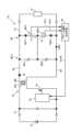
図4(a)は、ツェナーダイオード回路36、電流検出手段38(1),38(2)及びアラーム信号出力手段40の部分の具体的な回路構成の一例を示している。この例では、第一の電流検出手段38(1)は、エミッタが電源ライン28に接続され、ベースが第一のツェナーダイオード34(1)のカソードに接続されたPNPトランジスタ46と、PNPトランジスタ46のベースエミッタ間に補助的に接続された抵抗素子48とで構成される。第一の電流検出手段38(1)は、一定以上のツェナー電流Iz1が流れた時、それをPNPトランジスタ46がベースエミッタ間のPN接合で検出し、コレクタ電流(電流検出信号S(Iz1))を出力する動作を行う。
FIG. 4A shows an example of a specific circuit configuration of the
第二の電流検出手段38(2)は、アノードが第二ツェナーダイオード34(2)のアノードに接続され、カソードがグランドライン30に接続されたフォトダイオード50と、フォトダイオード50の両端に補助的に接続されたに抵抗素子52と、フォトダイオード50に光結合し、フォトダイオード50に入力された信号に対応した信号を出力するフォトトランジスタ54とで構成される。第二の電流検出手段38(2)は、一定以上のツェナー電流Iz2が流れた時、それをフォトダイオード50で検出し、フォトトランジスタ54がコレクタ電流(電流検出信号S(Iz2))を出力する動作を行う。
The second current detection means 38 ( 2 ) includes a
アラーム信号出力手段40は、PNPトランジスタ46と、PNPトランジスタ46のコレクタとフォトダイオード50のアノードとの間に接続されたコレクタ抵抗56と、フォトダイオード50と、フォトトランジスタ54とで構成される。アラーム信号出力手段40は、2つの電流検出手段38(1),38(2)の中の少なくとも一方が電流検出信号S(Iz1),S(Iz2)を出力すると、フォトトランジスタ54がコレクタ電流(アラーム信号S(ALM))を出力する動作を行う。
The alarm signal output means 40 comprises a
図4(b)は、電圧降下発生手段44(1)の具体的な回路構成の例を示している。上記のように、電圧降下発生手段44(1)は、双方向に電流を通過させることができ、ツェナー電流Iz1,Iz2が通過した時に、自己の両端に、ツェナー電流Iz1,Iz2の向きに応じて正方向又は負方向に電圧降下を発生させる素子又は回路網である。例えば、電圧降下発生手段44aは、1つの抵抗素子で構成した最もシンプルな例である。電圧降下発生手段44bは、ダイオード素子と抵抗素子との直列回路を2組用意し、これらを逆向きに並列接続した構成であり、電圧降下Vx1(Iz1が流れた時の電圧降下の大きさ)及び電圧降下Vx2(Iz2が流れた時の電圧降下の大きさ)を別々に調節できるので、電圧降下発生手段44aよりも設計の自由度が高い。 FIG. 4(b) shows an example of a specific circuit configuration of the voltage drop generating means 44(1). As described above, the voltage drop generating means 44(1) can pass current in both directions. A device or network that produces a voltage drop in the positive or negative direction across the For example, the voltage drop generating means 44a is the simplest example composed of one resistive element. The voltage drop generation means 44b has a configuration in which two sets of series circuits of a diode element and a resistance element are prepared and connected in parallel in opposite directions. and the voltage drop Vx2 (magnitude of voltage drop when Iz2 flows) can be adjusted separately, so the degree of design freedom is higher than that of the voltage drop generating means 44a.
電圧降下発生手段44cは、互いのアノード同士が接続されたダイオード素子とツェナーダイオード素子との直列回路を2組用意し、これらを逆向きに並列接続した構成であり、電圧降下発生手段44dは、複数個のダイオード素子を一方向に配した直列回路を2組用意し、これらを逆向きにして並列接続した構成である。電圧降下発生手段44cは、ツェナーダイオード素子を使用するので、電圧降下Vx1,Vx2を数ボルト以上に設定する場合に有利で、電圧降下発生手段44dは、ダイオード素子だけで構成するので、電圧降下Vx1,Vx2を1~3V程度の低い値に設定する場合に有利である。また、電圧降下発生手段44c,44dは、上記の電圧降下発生手段44a,44bよりも、さらに電圧降下Vx1,Vx2の調節が容易である。 The voltage drop generating means 44c has a configuration in which two sets of series circuits of a diode element and a Zener diode element whose anodes are connected to each other are prepared and connected in parallel in opposite directions. Two sets of series circuits, in which a plurality of diode elements are arranged in one direction, are prepared, and these are connected in parallel in opposite directions. Since the voltage drop generating means 44c uses a Zener diode element, it is advantageous when setting the voltage drops Vx1 and Vx2 to several volts or more. , Vx2 are set to low values of the order of 1 to 3V. Further, the voltage drop generating means 44c, 44d are easier to adjust the voltage drops Vx1, Vx2 than the voltage drop generating means 44a, 44b.
以上説明したように、電源装置42は、Vo上限値をツェナー電圧Vz1,Vz2と電圧降下Va1,Va2とで調節し、Vc上限値をツェナー電圧Vz1,Vz2と電圧降下Va1,Va2と電圧降下Vxとで調節できる構成になっており、過電圧検出機能及びコンデンサ故障検出機能の設計に使用できるパラメータの数が従来よりも多いので、2つの機能の設計をバランスよく行うことができる。しかも、図4に示すように、非常にシンプルな回路構成にすることができ、部品点数の増加やコストアップを最小限に抑えることができる。
As described above, the
なお、図2、図3の中に付した[数値例]は1つの設計例を示したものであり、出力電圧Voの目標値Vr等の条件が異なる場合であっても、同様の考え方で、過電圧検出機能及びコンデンサ故障検出機能の設計をバランスよく行うことができる。 Note that the [numerical examples] shown in FIGS. 2 and 3 show one design example. , the overvoltage detection function and the capacitor failure detection function can be designed in a well-balanced manner.
また、図1や図4の回路図では、ツェナーダイオード34(1),34(2)を保護するためにツェナー電流Iz1,Iz2の最大値を制限する電流制限抵抗が省略してあるが、例えばツェナーダイオード34(1)や34(2)と直列の位置に、比較的抵抗値の小さい電流制限抵抗を挿入することができる。ただし、電流制限抵抗を挿入すると、電流制限抵抗にツェナー電流Iz1,Iz2が流れた時に若干の電圧降下が発生し、過電圧検出及びコンデンサ短絡故障検出の精度に影響が出る可能性があるので、電流制限抵抗を挿入する場合は、電流制限抵抗に発生する電圧降下も考慮して設計するとよい。また、電流制限抵抗は、電流検出手段の一部(例えば、電流検出用抵抗)として使用する構成にしてもよい。 In the circuit diagrams of FIGS. 1 and 4, the current limiting resistors for limiting the maximum values of the Zener currents Iz1 and Iz2 are omitted to protect the Zener diodes 34(1) and 34(2). A current limiting resistor with a relatively small resistance value can be inserted in series with Zener diodes 34(1) and 34(2). However, if a current limiting resistor is inserted, a slight voltage drop will occur when Zener currents Iz1 and Iz2 flow through the current limiting resistor, which may affect the accuracy of overvoltage detection and capacitor short-circuit detection. When inserting a limiting resistor, the voltage drop that occurs in the current limiting resistor should also be taken into account in the design. Also, the current limiting resistor may be configured to be used as part of the current detection means (for example, a current detection resistor).
ツェナーダイオード34(1)は、ツェナー電圧Vz1を微調整するため、複数個のツェナーダイオード素子を直列接続して構成してもよい。ツェナーダイオード34(2)についても同様である。このような構成にしても、電源装置42が目的とする過電圧検出及びコンデンサ故障検出を実現することができる。
The Zener diode 34(1) may be configured by connecting a plurality of Zener diode elements in series in order to finely adjust the Zener voltage Vz1. The same is true for Zener diode 34(2). Even with such a configuration, the overvoltage detection and capacitor failure detection intended by the
その他、コンデンサ24(1)は、複数個のコンデンサ素子を並列接続して構成してもよい。コンデンサ24(2)についても同様である。電源装置42のコンデンサ故障検出機能は、コンデンサ24(1),24(2)のどちらか一方が短絡故障したことを検出することが目的であり、並列接続されたコンデンサ素子の中のどれが短絡故障しても、この目的を達成することができる。
Alternatively, the capacitor 24(1) may be configured by connecting a plurality of capacitor elements in parallel. The same is true for capacitor 24(2). The purpose of the capacitor failure detection function of the
次に、第一の実施形態の電源装置42の、第一及び第二の電流検出手段38(1),38(2)の配置を変更した2つの変形例を説明する。
Next, two modifications of the
第一の電流検出手段38(1)は、第一ツェナーダイオード34(1)に一定以上のツェナー電流Iz1が流れたことを検出する手段であり、回路の中のどの位置に設けるかは限定されない。同様に、第二の電流検出手段38(2)は、第二ツェナーダイオード34(2)に一定以上のツェナー電流Iz2が流れたことを検出する手段であり、回路の中のどの位置に設けるかは自由である。 The first current detection means 38(1) is a means for detecting that a Zener current Iz1 above a certain level has flowed through the first Zener diode 34(1), and there is no limitation as to where it is provided in the circuit. . Similarly, the second current detection means 38(2) is means for detecting that a Zener current Iz2 above a certain level has flowed through the second Zener diode 34(2). is free.
例えば、図5(a)に示す第一の変形例は、第一の電流検出手段38(1)を、第一ツェナーダイオード34(1)と直列の位置から、電圧降下発生手段44(1)と直列の位置に変更したものである。このように変更した場合も、図2、図3に示すように、各種の異常が発生した時に同様の動作が行われ、同様の効果が得られる。ただし、電流検出手段38(1)の配置を変更すると電圧降下Va1が発生する位置が変わるので、電圧降下Va1,Va2が無視できない場合は、設計時に留意する必要がある。 For example, a first modification shown in FIG. 5(a) moves the first current detection means 38(1) from a position in series with the first Zener diode 34(1) to the voltage drop generation means 44(1). It is changed to a position in series with. Even in the case of such a change, as shown in FIGS. 2 and 3, similar operations are performed when various kinds of abnormalities occur, and similar effects can be obtained. However, if the placement of the current detection means 38(1) is changed, the position at which the voltage drop Va1 occurs will change, so if the voltage drops Va1 and Va2 cannot be ignored, this must be taken into consideration during design.
図6は、第一の変形例の具体的な回路構成の一例を示しており、この電流検出手段38(1)は、電流検出素子44(1)に一定以上のツェナー電流Iz1が流れた時、それをPNPトランジスタ46がベースエミッタ間のPN接合で検出し、コレクタ電流(電流検出信号S(Iz1))を出力する動作を行う。ベースエミッタ間に接続されたダイオード57は、ツェナー電流Iz2が電圧降下発生手段44(1)に流れることができるようにするための電流バイパス用のダイオードで、PNPトランジスタ46のPN接合と逆向きに並列接続されている。
FIG. 6 shows an example of a specific circuit configuration of the first modified example. This current detection means 38(1) detects a , is detected by the
また、図5(b)に示す第二の変形例は、第二の電流検出手段38(2)を、第二ツェナーダイオード34(2)と直列の位置から、電圧降下発生手段44(1)と直列の位置に変更したものである。このように変更した場合も、図2、図3に示すように、各種の異常が発生した時に同様の動作が行われ、同様の効果が得られる。ただし、電流検出手段38(2)の配置を変更すると電圧降下Va2が発生する位置が変わるので、電圧降下Va1,Va2が無視できない場合は、設計時に留意する必要がある。 In addition, in the second modification shown in FIG. 5(b), the second current detecting means 38(2) is connected from the position in series with the second Zener diode 34(2) to the voltage drop generating means 44(1). It is changed to a position in series with. Even in the case of such a change, as shown in FIGS. 2 and 3, similar operations are performed when various kinds of abnormalities occur, and similar effects can be obtained. However, if the placement of the current detection means 38(2) is changed, the position where the voltage drop Va2 occurs will change, so if the voltage drops Va1 and Va2 cannot be ignored, it must be noted during design.
次に、本発明の電源装置の第二の実施形態について、図7、図8に基づいて説明する。ここで、第一の実施形態の電源装置42と同様の構成は、同一の符号を付して説明を省略する。
Next, a second embodiment of the power supply device of the present invention will be described with reference to FIGS. 7 and 8. FIG. Here, configurations similar to those of the
この実施形態の電源装置58は、電源装置42と同様に、直流の入力電源12から入力された入力電圧Viを直流の出力電圧Voに変換し、この出力電圧Voを装置の出力端に接続された負荷14に向けて出力する装置である。
The
電源装置58は、図7に示すように、電源ライン28の、第一のコンデンサ回路26(1)が接続されている位置(電源ライン28a)の前段に、インダクタ60と第二のコンデンサ回路26(2)(以下、単にコンデンサ回路26(2)と称する。)とが設けられ、コンデンサ回路26(2)、インダクタ60及びコンデンサにより、インダクタ60の前段の電源ライン28bに発生するスイッチング周波数のリップル電圧を吸収するπ型のローパスフィルタ62が構成されているという特徴がある。
As shown in FIG. 7, the
電源ライン28bとグランドライン30との間に接続されたコンデンサ回路26(2)は、第三及び第四コンデンサ24(3),24(4)(以下、単にコンデンサ24(3),24(4)と称する。)を上段側から順に直列接続した回路である。コンデンサ24(3),24(4)の容量比で定まる分圧比は、コンデンサ24(1),24(2)の容量比で定まる分圧比と同じに設定されている。個々のコンデンサの容量のバラツキや漏れ電流の影響で分圧比が変動する可能性がある時は、コンデンサ24(3),24(4)に図示しないバランス抵抗が並列接続される。
A capacitor circuit 26(2) connected between the
電源装置58の電源ラインは、スイッチング方式の電力変換回路の出力電圧Voが発生するラインであり、このラインに接続されるデカップリングコンデンサの容量が小さいと、スイッチング周波数Fswの大きいリップル電圧Vripが重畳してしまう。したがって、電源装置58では、出力電圧Voからリップル電圧Vripを吸収するためにローパスフィルタ62が設けられている。
The power supply line of the
さらに電源装置58は、コンデンサ24(3),24(4)の中点とツェナーダイオード34(1),34(2)の中点との間に第二の電圧降下発生手段44(2)(以下、単に電圧降下発生手段44(2)と称する。)が接続されている。電圧降下発生手段44(2)は、双方向に電流を通過させることができ、ツェナー電流Iz1,Iz2が通過した時に、自己の両端に、電圧降下発生手段44(1)と同じ大きさの正方向又は負方向に電圧降下を発生させる素子又は回路網である。具体的には、図4(b)に示す電圧降下発生手段44a~44dのような構成にすることができる。
次に、電源装置58が行うコンデンサ故障検出の動作と過電圧検出の動作について、図8に基づいて説明する。なお、図8の中の[数値例]は、説明を理解しやすくするために記載した典型的な設計例であり、この設計例では、出力電圧Voの目標値Vrが12V、コンデンサ24(1)~24(4)の耐電圧Vdcが16V、ツェナーダイオード34(1),34(2)のツェナー電圧Vzが6.9V、電流検出手段38(1),38(2)にツェナー電流Iz1,Iz2が流れた時の電圧降下Vaが0.6V、電圧降下発生手段44(1),44(2)にツェナー電流Iz1,Iz2が流れた時の電圧降下±Vxが±2.5Vとなっている。
Next, the capacitor failure detection operation and the overvoltage detection operation performed by the
また、電源ライン28bに発生するリップル電圧Vripは、負荷14に供給する出力電流Ioが大きい時で、振幅を4Vp-pとしている。リップル電圧Vripは、出力電流Ioの大小によって変化するという性質があり、例えば、出力電流Ioが非常に小さい時はVrip≒ゼロボルトであるが、出力電流Ioが大きくなるとVripが大きくなって4Vp-pになる。
The ripple voltage Vrip generated in the
図8(a)、(b)に示すように、正常動作中で出力電流Ioが大きい時、電源ライン28aに発生する出力電圧Voは、目標値Vr[12V]に制御された直流電圧であって、リップル電圧Vrip[4Vp-p]がほとんど重畳していない波形になる。一方、電源ライン28bの電圧Vkは、目標値Vr[12V]にリップル電圧Vrip[4Vp-p]が重畳した波形となり、インダクタ60の両端に電圧Vch≒Vrip[4Vp-p]が発生する。
As shown in FIGS. 8A and 8B, when the output current Io is large during normal operation, the output voltage Vo generated in the
コンデンサ24(1),24(2)の電圧Vc1,Vc2はVr/2[6V]となり、耐電圧Vdc[16V]に対して余裕がある。コンデンサ24(3),24(4)の電圧Vc3,Vc4はVr/2+Vrip/2[6V+2V]となり、耐電圧Vdc[16V]に対して余裕がある。また、ツェナーダイオード34(1),34(2)は導通せず、ツェナー電流Iz1,Iz2は流れない。したがって、電流検出手段38(1),38(2)は電流検出信号S(Iz1),S(Iz2)を出力せず、アラーム信号出力手段40はアラーム信号S(ALM)を出力しないので、制御回路32は、スイッチング素子18のオンオフ動作を継続させる。
The voltages Vc1 and Vc2 of the capacitors 24(1) and 24(2) are Vr/2 [6V], which is sufficient for the withstand voltage Vdc [16V]. The voltages Vc3 and Vc4 of the capacitors 24(3) and 24(4) are Vr/2+Vrip/2 [6V+2V], which is sufficient for the withstand voltage Vdc [16V]. Also, Zener diodes 34(1) and 34(2) do not conduct, and Zener currents Iz1 and Iz2 do not flow. Therefore, the current detection means 38(1) and 38(2) do not output the current detection signals S(Iz1) and S(Iz2), and the alarm signal output means 40 does not output the alarm signal S(ALM). The
次に、正常動作中の電源装置58に異常が発生した時の動作を説明するが、その前に、上記の電源装置42(ローパスフィルタ60を設けない電源装置)で発生し得る問題点について説明する。問題点とは、概して言うと、電源ライン28に一定以上に大きいリップル電圧Vripが発生すると、過電圧検出の精度が低下するということである。
Next, the operation when an abnormality occurs in the
電源装置42は、電源装置58と同様に、出力電流Ioが非常に小さい時はVrip≒ゼロボルトとなる。Vrip≒ゼロボルトであれば、正常動作中に制御回路32が故障して出力電圧Voが制御不能になった時、図3(b)に示すように、Vo上限値は2・Vz+2・Va[約15V≒Vr×1.25倍]となる。しかし、出力電流Ioが大きい時は、リップル電圧Vripが一定以上に大きくなり[4Vp-p]、ツェナー電流Iz1,Iz2が流れ始める条件が変化するので、Vo上限値が、概ね2・Vz+2・Va-Vrip/2[約13V≒Vr×1.08倍]まで低下する。
Vo上限値と目標値Vrとが近すぎると、正常動作中であっても、特定の条件の時に出力電圧VoがVo上限値を超え、電源装置42が誤停止してしまう可能性がある。例えば、Vo上限値が13Vで目標値Vrが12Vとすれば、出力電流Ioが急変して出力電圧Voが変動した時等に、電源装置42が誤停止してしまう可能性が高い。
If the Vo upper limit value and the target value Vr are too close, the output voltage Vo may exceed the Vo upper limit value even during normal operation, and the
この誤停止を回避するには、Vo上限値=2・Vz+2・Va-Vrip/2の中のVrip/2の影響を考慮してツェナー電圧Va[6.9V]を少し高い値[7.9V]に変更し、Vo上限値を目標値Vrの1.25~1.4倍程度[約15V≒Vr×1.25倍]に設定しなければならない。しかしながら、ツェナー電圧Vaを高くすると[7.9Vに変更すると]、出力電流Ioが非常に小さい時のVo上限値2・Vz+2・Vaが必要以上に高い値[約17V≒Vr×1.42倍]になってしまうので、ユーザの負荷14を確実に保護できない可能性が出てくる。
To avoid this erroneous stop, consider the effect of Vrip/2 in the Vo upper limit value = 2 Vz + 2 Va - Vrip/2 and set the Zener voltage Va [6.9V] to a slightly higher value [7.9V]. The Vo upper limit must be set to about 1.25 to 1.4 times the target value Vr [approximately 15 V ≒ Vr x 1.25 times]. However, if the Zener voltage Va is increased [changed to 7.9V], the Vo
このように、電源装置42(ローパスフィルタ60を設けない電源装置)の場合、電源ライン28に一定以上のリップル電圧Vripが発生すると、Vo上限値が出力電流Ioの大小によって変動し、過電圧検出の精度が低下してしまうので、ユーザの負荷14を確実に保護できない可能が出てくる。なお、一定以上のリップル電圧Vripが発生すると、コンデンサ24(1),24(2)の故障検出の精度も多少低下するが、コンデンサ24(1),24(2)を安全に保護できるように設定にすることは、それほど難しくはない。
Thus, in the case of the power supply device 42 (the power supply device without the low-pass filter 60), when the ripple voltage Vrip of a certain level or more occurs in the
これに対して、この実施形態の電源装置58の場合、図8(a)に示すように、ツェナーダイオード回路36が、リップル電圧Vripが除去された後の電源ライン28bに接続されているので、Vo上限値が出力電流Ioの大小によって変動することはない。したがって、出力電圧Voの過電圧を検出する精度が一定に保持され、ユーザの負荷14を確実に保護することができる。なお、電源装置58においては、電源装置42の場合と同様に、リップル電圧Vripの影響でコンデンサ24(3),24(4)の故障検出の精度が多少低下することは避けられない。しかし、図8の中に記した[数値例]から分かるように、コンデンサ24(3),24(4)を安全に保護できるように設定にすることは十分に可能である。
In contrast, in the case of the
以上説明したように、第二の実施形態の電源装置58によれば、第一の実施形態の電源装置42と同様の作用効果を得ることができ、さらに、電源ライン28bに発生するリップル電圧Vripの影響で過電圧検出の精度が低下する心配がなく、ユーザの負荷14を確実に保護することができる。また、非常にシンプルな構成でありながら、第一及び第二コンデンサ24(1),24(2)と第三及び第四コンデンサ24(3),24(4)の両方を安全に保護することができる。なお、図8の中に付した[数値例]は1つの設計例を示したものであり、出力電圧Voの目標値Vrやリップル電圧Vripの値等の条件が異なる場合であっても、同様の考え方で、過電圧検出機能とコンデンサ故障検出機能の設計を容易に行うことができる。
As described above, according to the
なお、本発明の電源装置は、上記実施形態に限定されるものではない。例えば、上記の電源装置42の電力変換回路はフライバックコンバータ16(絶縁型のコンバータ)であるが、電力変換回路の構成は特に限定されず、例えば図9に示す電源装置64のように、力率改善用昇圧チョッパ66(非絶縁型のコンバータ)でもよい。電源装置64は、力率改善用昇圧チョッパ66の前段に全波整流型の整流回路68を有し、交流の入力電源70から入力された商用交流電圧を整流回路68で脈流の入力電圧Viを生成した後、脈流の入力電圧Viを力率改善用昇圧チョッパ66で直流の出力電圧Voに変換し、出力端に接続された負荷14に向けて出力する。そして、制御回路32が、入力電源64から入力される入力電流の波形が商用交流電圧と相似形にする制御を行う。
It should be noted that the power supply device of the present invention is not limited to the above embodiments. For example, the power conversion circuit of the
電源装置64の場合、電源装置42と同様に、出力電圧Voが発生するラインが電源ライン28となり、出力電圧Voのグランドとなるラインがグランドライン30となる。そして、電力変換回路が非絶縁型なので、制御回路32のグランドもグランドライン30に接続されることになる。したがって、第二の電流検出手段38(2)及びアラーム信号出力手段40を構成する時は、図4(a)に示すフォトダイオード50及びフォトトランジスタ56の部分(信号を絶縁する部分)を、例えば図10に示すようなNPNトランジスタ72に置き換えることができ、よりシンプルな構成にすることができる。
In the case of the
第一及び第二の電流検出手段及びアラーム信号出力手段の構成は、図4(a)や図10に示す回路構成に限定されるものではなく、本発明が目的とする動作が可能な範囲で自由に変更することができる。また、電源ライン(過電圧検出の対象となるライン)は、必ずしもスイッチング方式の電力変換回路の出力電圧が発生するラインである必要はなく、例えばシリーズレギュレータの出力電圧が発生するライン等であってもよい。 The configurations of the first and second current detection means and the alarm signal output means are not limited to the circuit configurations shown in FIGS. You can change it freely. Also, the power supply line (the line targeted for overvoltage detection) does not necessarily have to be a line that generates the output voltage of a switching power conversion circuit. good.
10,42,58,64 電源装置
16 フライバックコンバータ(スイッチング方式の電力変換回路)
24(1) 第一コンデンサ
24(2) 第二コンデンサ
24(3) 第三コンデンサ
24(4) 第四コンデンサ
26(1) 第一のコンデンサ回路
26(2) 第二のコンデンサ回路
28,28a,28b 電源ライン
30 グランドライン
32 制御回路
34(1) 第一ツェナーダイオード
34(2) 第二ツェナーダイオード
36 ツェナーダイオード回路
38(1) 第一の電流検出手段
38(2) 第二の電流検出手段
40 アラーム信号出力手段
44(1),44a,44b,44c,44d 第一の電圧降下発生手段
44(2),44a,44b,44c,44d 第二の電圧降下発生手段
46 PNPトランジスタ
50 フォトダイオード
54 コレクタ抵抗
56 フォトトランジスタ
60 インダクタ
62 π型のローパスフィルタ
66 力率改善用昇圧チョッパ(スイッチング方式の電力変換回路)
10, 42, 58, 64
24(1) First capacitor 24(2) Second capacitor 24(3) Third capacitor 24(4) Fourth capacitor 26(1) First capacitor circuit 26(2)
Claims (8)
第一コンデンサ及び第二コンデンサを上段側から順に配して直列接続した回路で成り、前記電源ラインと前記グランドラインとの間に接続された第一のコンデンサ回路と、
第一ツェナーダイオード及び第二ツェナーダイオードを上段側から順に配して直列接続した回路で成り、前記電源ラインと前記グランドラインとの間に接続されたツェナーダイオード回路と、
前記第一及び第二コンデンサの中点と前記第一及び第二ツェナーダイオードの中点との間に接続された第一の電圧降下発生手段と、
前記第一ツェナーダイオードに一定以上のツェナー電流が流れたことを検出する第一の電流検出手段と、
前記第二のツェナーダイオードに一定以上のツェナー電流が流れたことを検出する第二の電流検出手段と、
前記2つの電流検出手段の中の少なくとも一方で、前記一定以上のツェナー電流が流れたことが検出された時、アラーム信号を出力するアラーム信号出力手段とを備え、
前記第一ツェナーダイオードは、カソードが前記電源ラインに向けて配され、前記第二ツェナーダイオードは、カソードが前記第一ツェナーダイオードに向けて配されており、
前記第一の電圧降下発生手段は、双方向に電流を通過させることができ、前記ツェナー電流が通過した時に、自己の両端に、当該ツェナー電流の向きに応じて正方向又は負方向に電圧降下を発生させるものであり、
前記第一の電流検出手段は、エミッタが前記電源ラインに接続され、ベースが前記第一ツェナーダイオードのカソードに接続されたPNPトランジスタにより構成され、
前記第二の電流検出手段は、アノードが前記第二ツェナーダイオードのアノードに接続され、カソードが前記グランドラインに接続されたフォトダイオードと、前記フォトダイオードに光結合し、前記フォトダイオードに入力された信号に対応した信号を出力するフォトトランジスタとで構成され、
前記アラーム信号出力手段は、前記PNPトランジスタと、前記PNPトランジスタのコレクタと前記フォトダイオードのアノードとの間に接続されたコレクタ抵抗と、前記フォトダイオードと、前記フォトトランジスタとで構成されることを特徴とする電源装置。 a power supply line and a ground line;
a first capacitor circuit composed of a circuit in which a first capacitor and a second capacitor are arranged in order from the upper stage and connected in series, the first capacitor circuit being connected between the power supply line and the ground line;
a Zener diode circuit comprising a circuit in which a first Zener diode and a second Zener diode are arranged in order from the top and connected in series, the circuit being connected between the power supply line and the ground line;
a first voltage drop generating means connected between the midpoint of the first and second capacitors and the midpoint of the first and second Zener diodes;
a first current detection means for detecting that a Zener current exceeding a certain level has flowed through the first Zener diode;
a second current detection means for detecting that a Zener current exceeding a certain level has flowed through the second Zener diode;
alarm signal output means for outputting an alarm signal when at least one of the two current detection means detects that a Zener current exceeding a certain level has flowed;
The first Zener diode has a cathode facing the power supply line, and the second Zener diode has a cathode facing the first Zener diode,
The first voltage drop generating means is capable of passing current in both directions, and when the Zener current passes through it, it produces a voltage drop in the positive direction or the negative direction depending on the direction of the Zener current. and
the first current detection means is composed of a PNP transistor having an emitter connected to the power supply line and a base connected to the cathode of the first Zener diode;
The second current detection means includes a photodiode having an anode connected to the anode of the second Zener diode and a cathode connected to the ground line, and a photodiode optically coupled to the photodiode and input to the photodiode. It consists of a phototransistor that outputs a signal corresponding to the signal,
The alarm signal output means comprises the PNP transistor, a collector resistor connected between the collector of the PNP transistor and the anode of the photodiode, the photodiode, and the phototransistor. and power supply.
直流の出力電圧を生成し、この出力電圧を前記電源ラインに供給するスイッチング方式の電力変換回路と、
第一コンデンサ及び第二コンデンサを上段側から順に配して直列接続した回路で成り、前記電源ラインと前記グランドラインとの間に接続された第一のコンデンサ回路と、
第一ツェナーダイオード及び第二ツェナーダイオードを上段側から順に配して直列接続した回路で成り、前記電源ラインと前記グランドラインとの間に接続されたツェナーダイオード回路と、
前記第一及び第二コンデンサの中点と前記第一及び第二ツェナーダイオードの中点との間に接続された第一の電圧降下発生手段と、
前記第一ツェナーダイオードに一定以上のツェナー電流が流れたことを検出する第一の電流検出手段と、
前記第二のツェナーダイオードに一定以上のツェナー電流が流れたことを検出する第二の電流検出手段と、
前記2つの電流検出手段の中の少なくとも一方で、前記一定以上のツェナー電流が流れたことが検出された時、アラーム信号を出力するアラーム信号出力手段とを備え、
前記第一ツェナーダイオードは、カソードが前記電源ラインに向けて配され、前記第二ツェナーダイオードは、カソードが前記第一ツェナーダイオードに向けて配されており、
前記第一の電圧降下発生手段は、双方向に電流を通過させることができ、前記ツェナー電流が通過した時に、自己の両端に、当該ツェナー電流の向きに応じて正方向又は負方向に電圧降下を発生させるものであり、
前記電源ラインの、前記第一のコンデンサ回路が接続されている位置の前段に、第二のコンデンサ回路及びインダクタが設けられ、前記第二のコンデンサ回路、前記インダクタ及び前記第一のコンデンサ回路により、前記電源ラインに発生するスイッチング周波数のリップル電圧を吸収するπ型のローパスフィルタが構成され、
前記第二のコンデンサ回路は、第三コンデンサ及び第四コンデンサを上段側から順に配して直列接続した回路で成り、前記電源ラインの前記ローパスフィルタの入力端の位置と前記グランドラインとの間に接続され、前記第三及び第四コンデンサの容量比で定まる分圧比は、前記第一及び第二コンデンサの容量比で定まる分圧比と同じに設定されており、
前記第三及び第四コンデンサの中点と前記第一及び第二ツェナーダイオードの中点との間に第二の電圧降下発生手段が接続され、前記第二の電圧降下発生手段は、双方向に電流を通過させることができ、前記ツェナー電流が通過した時に、自己の両端に、前記第一の電圧降下発生手段と同じ大きさの正方向又は負方向に電圧降下を発生させるものであることを特徴とする電源装置。 a power supply line and a ground line;
a switching power conversion circuit that generates a DC output voltage and supplies the output voltage to the power supply line;
a first capacitor circuit composed of a circuit in which a first capacitor and a second capacitor are arranged in order from the upper stage and connected in series, the first capacitor circuit being connected between the power supply line and the ground line;
a Zener diode circuit comprising a circuit in which a first Zener diode and a second Zener diode are arranged in order from the top and connected in series, the circuit being connected between the power supply line and the ground line;
a first voltage drop generating means connected between the midpoint of the first and second capacitors and the midpoint of the first and second Zener diodes;
a first current detection means for detecting that a Zener current exceeding a certain level has flowed through the first Zener diode;
a second current detection means for detecting that a Zener current exceeding a certain level has flowed through the second Zener diode;
alarm signal output means for outputting an alarm signal when at least one of the two current detection means detects that a Zener current exceeding a certain level has flowed;
The first Zener diode has a cathode facing the power supply line, and the second Zener diode has a cathode facing the first Zener diode,
The first voltage drop generating means is capable of passing current in both directions, and when the Zener current passes through it, it produces a voltage drop in the positive direction or the negative direction depending on the direction of the Zener current. and
A second capacitor circuit and an inductor are provided on the power supply line before the position where the first capacitor circuit is connected, and the second capacitor circuit, the inductor and the first capacitor circuit provide: A π-type low-pass filter is configured to absorb a switching frequency ripple voltage generated in the power supply line,
The second capacitor circuit is composed of a circuit in which a third capacitor and a fourth capacitor are arranged in order from the upper stage and connected in series, and is located between the position of the input end of the low-pass filter of the power supply line and the ground line. A voltage division ratio determined by a capacitance ratio of the third and fourth capacitors connected is set to be the same as a voltage division ratio determined by a capacitance ratio of the first and second capacitors,
A second voltage drop generating means is connected between the midpoint of the third and fourth capacitors and the midpoint of the first and second Zener diodes, the second voltage drop generating means bidirectionally It is capable of passing a current, and when the Zener current passes through it, it generates a voltage drop in the positive direction or the negative direction of the same magnitude as the first voltage drop generating means at both ends of itself. A power supply characterized by:
前記第二の電流検出手段は、アノードが前記第二ツェナーダイオードのアノードに接続され、カソードが前記グランドラインに接続されたフォトダイオードと、前記フォトダイオードに光結合し、前記フォトダイオードに入力された信号に対応した信号を出力するフォトトランジスタとで構成され、
前記アラーム信号出力手段は、前記PNPトランジスタと、前記PNPトランジスタのコレクタと前記フォトダイオードのアノードとの間に接続されたコレクタ抵抗と、前記フォトダイオードと、前記フォトトランジスタとで構成される請求項4記載の電源装置。 the first current detection means is composed of a PNP transistor having an emitter connected to the power supply line and a base connected to the cathode of the first Zener diode;
The second current detection means includes a photodiode having an anode connected to the anode of the second Zener diode and a cathode connected to the ground line, and a photodiode optically coupled to the photodiode and input to the photodiode. It consists of a phototransistor that outputs a signal corresponding to the signal,
5. The alarm signal output means comprises the PNP transistor, a collector resistor connected between the collector of the PNP transistor and the anode of the photodiode, the photodiode, and the phototransistor. Power supply as described .
前記第二のコンデンサ回路を構成する前記第三及び第四コンデンサには、前記第三及び第四コンデンサの容量比で定まる分圧比を安定化させるためのバランス抵抗が並列接続されている請求項4又は5記載の電源装置。 Balance resistors are connected in parallel to the first and second capacitors constituting the first capacitor circuit for stabilizing the voltage division ratio determined by the capacitance ratio of the first and second capacitors,
5. A balance resistor is connected in parallel to said third and fourth capacitors constituting said second capacitor circuit for stabilizing a voltage division ratio determined by a capacitance ratio of said third and fourth capacitors. Or the power supply device according to 5.
Priority Applications (1)
| Application Number | Priority Date | Filing Date | Title |
|---|---|---|---|
| JP2020176645A JP7319954B2 (en) | 2020-10-21 | 2020-10-21 | power supply |
Applications Claiming Priority (1)
| Application Number | Priority Date | Filing Date | Title |
|---|---|---|---|
| JP2020176645A JP7319954B2 (en) | 2020-10-21 | 2020-10-21 | power supply |
Publications (2)
| Publication Number | Publication Date |
|---|---|
| JP2022067826A JP2022067826A (en) | 2022-05-09 |
| JP7319954B2 true JP7319954B2 (en) | 2023-08-02 |
Family
ID=81455980
Family Applications (1)
| Application Number | Title | Priority Date | Filing Date |
|---|---|---|---|
| JP2020176645A Active JP7319954B2 (en) | 2020-10-21 | 2020-10-21 | power supply |
Country Status (1)
| Country | Link |
|---|---|
| JP (1) | JP7319954B2 (en) |
Citations (7)
| Publication number | Priority date | Publication date | Assignee | Title |
|---|---|---|---|---|
| JP2000350465A (en) | 1999-06-01 | 2000-12-15 | Yaskawa Electric Corp | 3-level inverter |
| JP2005012854A (en) | 2003-06-16 | 2005-01-13 | Mitsubishi Electric Corp | Capacitor voltage divider circuit |
| WO2012164785A1 (en) | 2011-05-27 | 2012-12-06 | パナソニック株式会社 | Lighting circuit and lamp |
| JP2017192219A (en) | 2016-04-14 | 2017-10-19 | 富士電機株式会社 | 3 level chopper device |
| JP2019092284A (en) | 2017-11-14 | 2019-06-13 | 富士電機株式会社 | Step-down chopper circuit |
| JP2019213283A (en) | 2018-05-31 | 2019-12-12 | ファナック株式会社 | Motor drive device having DC link capacitor short-circuit determination unit |
| JP2020162248A (en) | 2019-03-26 | 2020-10-01 | ローム株式会社 | Dc/dc converter control circuit, control method, and electronic device |
Family Cites Families (1)
| Publication number | Priority date | Publication date | Assignee | Title |
|---|---|---|---|---|
| JPH04111289U (en) * | 1991-03-06 | 1992-09-28 | テイーデイーケイ株式会社 | power circuit |
-
2020
- 2020-10-21 JP JP2020176645A patent/JP7319954B2/en active Active
Patent Citations (7)
| Publication number | Priority date | Publication date | Assignee | Title |
|---|---|---|---|---|
| JP2000350465A (en) | 1999-06-01 | 2000-12-15 | Yaskawa Electric Corp | 3-level inverter |
| JP2005012854A (en) | 2003-06-16 | 2005-01-13 | Mitsubishi Electric Corp | Capacitor voltage divider circuit |
| WO2012164785A1 (en) | 2011-05-27 | 2012-12-06 | パナソニック株式会社 | Lighting circuit and lamp |
| JP2017192219A (en) | 2016-04-14 | 2017-10-19 | 富士電機株式会社 | 3 level chopper device |
| JP2019092284A (en) | 2017-11-14 | 2019-06-13 | 富士電機株式会社 | Step-down chopper circuit |
| JP2019213283A (en) | 2018-05-31 | 2019-12-12 | ファナック株式会社 | Motor drive device having DC link capacitor short-circuit determination unit |
| JP2020162248A (en) | 2019-03-26 | 2020-10-01 | ローム株式会社 | Dc/dc converter control circuit, control method, and electronic device |
Also Published As
| Publication number | Publication date |
|---|---|
| JP2022067826A (en) | 2022-05-09 |
Similar Documents
| Publication | Publication Date | Title |
|---|---|---|
| KR100904299B1 (en) | Power factor correction circuit and its driving method | |
| US9502963B2 (en) | Switching power supply device, switching power supply control method and electronic apparatus | |
| TWI501533B (en) | An off-line voltage regulator, off-line regulator integrated circuit and voltage convert method thereof | |
| US8242765B2 (en) | Switching power supply device and semiconductor device used for the same | |
| US7522398B2 (en) | Method and apparatus for overcurrent protection in DC-DC power converters | |
| JP5056395B2 (en) | Switching power supply | |
| US20170070142A1 (en) | Input and output overvoltage protection in a power converter | |
| US12328063B2 (en) | Totem pole power factor correction circuit | |
| US20040027096A1 (en) | Auxiliary circuit for power factor corrector having self-power supplying and zero current detection mechanisms | |
| US20110051462A1 (en) | Power factor improvement circuit | |
| JP5282067B2 (en) | Power factor correction circuit and start-up operation control method thereof | |
| JPWO2020071011A1 (en) | Power control device and power control method | |
| WO2003092145A1 (en) | System and method for providing power factor correction | |
| CN103904621B (en) | Current-limiting protection with self-recovering function and short-circuit protection circuit | |
| JP7319954B2 (en) | power supply | |
| KR101055055B1 (en) | Power Factor Correction Circuit of Power Supply | |
| KR20200015380A (en) | Power supply circuit | |
| US12113434B2 (en) | Power supply apparatus and discharge method thereof | |
| CN206820650U (en) | A kind of switching power circuit | |
| JP6561321B2 (en) | Switching power supply | |
| CN115065228A (en) | Output sharing type industrial power supply | |
| JP6613938B2 (en) | LED power supply device and LED lighting device | |
| US11881772B2 (en) | Power supply device with discharge control | |
| US20240048046A1 (en) | High efficiency boost power factor correction circuit having shared pin and conversion control circuit thereof | |
| CN107786106B (en) | Buck chopper type switching power unit |
Legal Events
| Date | Code | Title | Description |
|---|---|---|---|
| A80 | Written request to apply exceptions to lack of novelty of invention |
Free format text: JAPANESE INTERMEDIATE CODE: A80 Effective date: 20201028 |
|
| A521 | Request for written amendment filed |
Free format text: JAPANESE INTERMEDIATE CODE: A523 Effective date: 20201202 |
|
| A621 | Written request for application examination |
Free format text: JAPANESE INTERMEDIATE CODE: A621 Effective date: 20220606 |
|
| A977 | Report on retrieval |
Free format text: JAPANESE INTERMEDIATE CODE: A971007 Effective date: 20230228 |
|
| A131 | Notification of reasons for refusal |
Free format text: JAPANESE INTERMEDIATE CODE: A131 Effective date: 20230307 |
|
| A521 | Request for written amendment filed |
Free format text: JAPANESE INTERMEDIATE CODE: A523 Effective date: 20230331 |
|
| TRDD | Decision of grant or rejection written | ||
| A01 | Written decision to grant a patent or to grant a registration (utility model) |
Free format text: JAPANESE INTERMEDIATE CODE: A01 Effective date: 20230705 |
|
| A61 | First payment of annual fees (during grant procedure) |
Free format text: JAPANESE INTERMEDIATE CODE: A61 Effective date: 20230721 |
|
| R150 | Certificate of patent or registration of utility model |
Ref document number: 7319954 Country of ref document: JP Free format text: JAPANESE INTERMEDIATE CODE: R150 |